Technical Field Of The Invention
The present invention is directed, in general, to
electronic circuit packaging and, more specifically, to an
electronic circuit with heat generating components in
which a relatively high thermal conductivity molded insert
is encapsulated with the components to improve removal of
heat from the components.
Background Of The Invention
To simplify the assembly of electronic devices,
electronic components are frequently furnished to
manufacturers in the form of preassembled modules
containing whole circuits for performing a given function.
The modules can then be advantageously handled in the
assembly line as single parts of a larger whole,
substantially speeding and simplifying the overall
assembly process.
Power supplies adapt well to this preassembled module
concept. Manufacturers of electronic systems (such as
computers and telephone switches) therefore commonly
acquire power supplies as preassembled modules from third
party suppliers, rather than build them themselves. To
protect the components and interconnections within the
preassembled modules from environmental and handling
damage, and to render them easier to handle during the
assembly process, the modules are frequently encapsulated
(or "potted") prior to further assembly.
Power supplies have shrunk in size and grown in
power-handling capability over the years. Unfortunately,
the resulting increase in power-handling capacity per unit
of circuit volume (power density) has made such power
supplies evermore difficult to encapsulate.
In general, encapsulating electronic components that
require substantial heat removal has proven to be an
intransigent problem. Ordinary potting materials do not
have a coefficient of thermal conductivity sufficient to
accommodate some of today's high thermal density
components. Potting materials that have a high
coefficient of thermal conductivity tend to be too
viscous, resulting in the formation of cavities in the
material. Guaranteeing the absence of cavities requires
substantial time and care, resulting in a marked (perhaps
four-fold) increase in manufacturing time. Even given the
extra time, encapsulating machines tend to jam in their
attempts to manage the thicker material, forcing the
assembly line to be interrupted so the machines can be
cleaned and restarted.
Accordingly, what is needed in the art is an improved
way to encapsulate power supplies and heat-producing
electronic components in general.
Summary Of The Invention
To address the above-discussed deficiencies of the
prior art, the present invention provides an encapsulant
structure for retaining an electronic circuit having heat-generating
components within a case that at least
partially surrounds the electronic circuit. In one
advantageous embodiment, the encapsulant structure
provides for a thermally conductive insert to be located
within the case proximate the heat-generating components.
The insert increases the heat transfer efficiency from the
electronic circuit to the case. In a related embodiment,
the encapsulant -structure further includes a potting
material, having a lower coefficient of thermal
conductivity than the insert, that encapsulates both the
electronic circuit and the insert.
The present invention therefore, in broad scope,
introduces the concept of placing an insert that has a
high rate of thermal conductivity in an encapsulated
circuit proximate to the heat generating components in
such circuit. Because the heat transfer characteristics
of the insert are better than the potting material used to
encapsulate the circuit, heat generated by the components
in the circuit can be more efficiently conducted to the
case of the encapsulated circuit, where it can be
transferred to the surrounding ambient air.
In one embodiment of the invention, the thermally
conductive insert has a general topographical conformity
to the electronic circuit, which topographic shape places
the insert in closer proximity to the heat generating
components. In another embodiment of the invention, the
thermally conductive insert is premolded. In still
another embodiment, the thermally conductive insert is
flexible and compliant, which advantageously permits the
insert to be pressed around the encapsulated electronic
circuit and eases the assembly process of manufacturing
the encapsulant structure. In another embodiment of the
invention, a plurality of thermally conductive inserts are
located within the case.
Another aspect of the invention provides for the
encapsulant structure to have a thermally conductive
insert precut from sheets of material having a coefficient
of thermal conductivity that is greater than the potting
material. In a particularly favorable embodiment the
insert can be placed in the case by a machine, such as a
pick-and-place machine. In yet another embodiment, the
precut thermally conductive insert is compressible. This
is also particularly beneficial as the insert can be
pressed around the components to assure close proximity
between the insert and the heat generating components in
the circuit.
The present invention also provides for a method of
manufacturing an encapsulated electronic circuit having
heat-generating components. The method, in one
embodiment, comprises the provision of a case to at least
partially surround the electronic circuit. A thermally
conductive insert is located within the case proximate to
the heat-generating components to increase a heat transfer
efficiency from the electronic circuit to the case. In a
related embodiment, the method further includes locating
potting material, having a lower coefficient of thermal
conductivity than the insert, in the case to encapsulate
both the electronic circuit and the insert.
A particularly useful embodiment of the method of
manufacturing calls for providing a case to at least
partially surround the electronic circuit containing heat
generating components. An initial layer of potting
material is placed within the case and quick-cured. A
thermally conductive insert is located within the case
proximate the heat-generating components. Potting
material, having a lower coefficient of thermal
conductivity than the insert, in then located in the case
to encapsulate both the electronic circuit and the insert.
Another aspect of this method provides for the initial
layer of potting material within the case to have a
thickness of about 2 to 6 millimeters. Yet another aspect
of this method is to quick cure wherein the initial layer
of potting material within the case using a process
selected from the group of an ultraviolet process and a
microwave process.
The present invention also provides for an electronic
device, comprised of a substrate adapted to receive
electronic components and an encapsulant structure for an
electronic circuit mounted on the substrate and having
heat generating components. The encapsulant structure
includes, in one embodiment, a case at least partially
surrounding the electronic circuit and a thermally
conductive insert located within the case proximate the
heat-generating components. In a related embodiment, the
encapsulant structure further includes a potting material,
having a lower coefficient of thermal conductivity than
the insert, to encapsulate both the electronic circuit and
the insert so that the insert may increase the heat
transfer efficiency from the electronic circuit to the
case.
The foregoing has outlined, rather broadly, preferred
and alternative features of the present invention so that
those skilled in the pertinent art may better understand
the detailed description of the invention that follows.
Additional features of the invention will be described
hereinafter that form the subject of the claims of the
invention. Those skilled in the pertinent art should
appreciate that they can readily use the disclosed
conception and specific embodiment as a basis for
designing or modifying other structures for carrying out
the same purposes of the present invention. Those skilled
in the pertinent art should also realize that such
equivalent constructions do not depart from the spirit and
scope of the invention in its broadest form.
Brief Description Of The Drawings
For a more complete understanding of the present
invention, reference is now made to the following
descriptions taken in conjunction with the accompanying
drawings, in which:
Detailed Description
Referring initially to FIGURE 1, illustrated is an
exploded isometric view of an embodiment of an electronic
device 100 constructed in accordance with the principles
of the present invention. The electronic device 100
(e.g., a power supply) includes an electronic circuit 110
having heat generating components (one of which is
designated 115). In the illustrated embodiment, the
electronic circuit 110 includes first and second
substrates (such as printed wiring boards) adapted to
receive electronic components (including the heat
generating components 115). Of course, the electronic
circuit 110 may be constructed on a single printed wiring
board, or one or more of other types of substrates, as an
application may dictate.
The electronic device 100 further includes a case 120
that at least partially surrounds the electronic circuit
110. The electronic device 100 still further includes an
encapsulant structure that retains the electronic circuit
110 within the case 120. In the illustrated embodiment,
the encapsulant structure includes a thermally conductive
insert 130 that is located within the case 120. The
thermally conductive insert 130 may comprise a polymer
material, such as silicone or silicone gel, that exhibits
a superior coefficient of thermal conductivity. The
encapsulant structure further includes a potting material
(difficult to illustrate given its amorphous nature, but
indicated conceptually in FIGURE 1 by a broken level fill
line 140) having a lower coefficient of thermal
conductivity than the thermally conductive insert 130. Of
course, the potting material is not necessary to the
present invention.
By providing the electronic device 100 as a modular,
self-contained subassembly, manufacturers of electronic
equipment can include the electronic device 100 as a
single discrete part as part of a larger electronic
system. Such electronic devices 100 can be purchased in
an encapsulated modular form from third party suppliers.
Alternatively, the manufacturer itself can make the
electronic circuit 110. As previously stated, power
supplies, such as board mounted power supplies, are
frequently furnished in such an encapsulated modular form.
When assembled, the electronic circuit 110 is located
in the case 120, which substantially surrounds the
electronic circuit 110. The thermally conductive insert
130 is located within the case 120 proximate the heat
generating components 115 of the electronic circuit 110.
The case 120 is then filled to a desired level with the
potting material. The potting material in the illustrated
embodiment has a relatively low viscosity (the better to
dispense the potting material into the case 120).
Such potting material is usually poured by an
assembly machine into the case 120 and allowed to cure.
After the potting material hardens, the electronic device
100 becomes essentially a solid block, with electrical
terminals or conductors projecting therefrom. Because the
electronic device 100 is now a unitary structure, it can
be handled as discrete part during the manufacturing
process, even though, underneath the potting material, the
thermally conductive insert 130 and the case 120, the
electronic device 100 remains an electronic circuit 110
made up of multiple discrete components.
Because the standard polymer potting material
generally used to encapsulate the electronic circuit 110
to form the electronic device 100 has a limited capacity
to conduct heat, the present invention provides for the
thermally conductive insert 130 to have a higher
coefficient of thermal conductivity than the surrounding
potting material. By placing the thermally conductive
insert 130 proximate the heat generating components 115 on
the electronic circuit 110, heat from the heat generating
components 115 may be conducted by the thermally
conductive insert 130 to the case 120. In situations
where the thermally conductive insert 130 is in contact
with both the heat generating component 115 and the case
120, a direct route is provided to conduct heat from the
heat generating components 115 to the case 120.
In the illustrated embodiment of the present
invention, the thermally conductive insert 130 has a
general topographical conformity with the components
(including the heat generating component 115) of the
electronic circuit 110. The thermally conductive insert
130 has topographical features (one of which takes the
form of an indentation 131) that allow the thermally
conductive insert 130 to fit around the heat generating
components 115. This is advantageous because it permits
the thermally conductive insert 130 to be in close contact
with the heat generating components 115 and thereby
improves the transfer of heat from the heat generating
components 115 to the thermally conductive insert 130. In
one embodiment of the present invention, wherein the
thermally conductive insert 130 comprises silicone, the
thermally conductive insert 130 may be premolded. The
indentation 131 may thus be formed as part of the molding
process. In an alternative embodiment of the present
invention, wherein the thermally conductive insert 130
comprises silicone gel, the thermally conductive insert
130 may be available in sheet form, and may need to be cut
from the sheet.
Electronic components, such as the heat generating
components 115 used in electrical circuits 110, frequently
have an irregular shape. These irregular shapes, in
combination with the multiplicity of smaller components
usually found on the electronic circuit 110, may make it
difficult and impractical to mold perfectly correct
topographical features (such as the indentation 131) in
the thermally conductive insert 130. One particularly
beneficial embodiment of the invention addresses this
problem by providing for the thermally conductive insert
130 to be flexible or compliant. This permits the
thermally conductive insert 130 to be pressed down around
the electrical circuit 110 and its irregularly shaped
components during the assembly process. The thermally
conductive insert 130 may thus conform to the topography
of the electronic circuit 110 in this manner.
Turning now to FIGURE 2, illustrated is an exploded
isometric view of another embodiment of an electronic
device 200 constructed in accordance with the principles
of the present invention. The electronic device 200
employs an encapsulant structure having a plurality of
thermally conductive inserts 210 located within a case
220. Frequently, the structure of an electronic circuit
230 employed by the electronic device 200 requires that a
number of thermally conductive inserts 210 be employed.
For example, some electronic circuits 230 may have a
design that requires a stack of the thermally conductive
inserts 210 to provide a complete thermal path between
heat generating components 235 employed in the electronic
circuit 230 and the case 220. In other applications, the
electronic circuit 230 may have widely separated heat
generating components 235 or may be constructed on
multiple printed wiring boards. In such instances, it may
be efficient to use a multiple thermally conductive
inserts 210 to conduct heat from the heat generating
components 235 to the case 220.
In those cases where a flexible and compliant
thermally conductive insert 210 (e.g., silicone gel) is
used, some assembly machines may have handling problems,
such as difficulty in picking up the thermally conductive
inserts 210 and placing them into the cases 220 to form
the electronic devices 200 described herein. To address
this problem, the thermally conductive inserts 210 may be
manufactured from a stiffer material, such as silicone.
The thermally conductive inserts 210 may be precut from
sheets of the material. These precut thermally conductive
inserts 210 advantageously exhibit a coefficient of
thermal conductivity greater than the surrounding potting
material, but the relatively stiff composition of the
thermally conductive inserts 210 can permit easy handling
by the assembly machines, such as pick and place machines.
One embodiment of the invention provides for the
precut thermally conductive inserts 210 to be cut from
sheets of a compressible material. When the thermally
conductive insert 210 is then placed into a case 220, the
thermally conductive insert 210 can be pressed around the
electronic circuit 230 and its heat generating components
235 to provide for positive contact between the heat
generating components 235 and the thermally conductive
insert 210. This feature provides for both ease of
assembly and for more efficient heat control.
The present invention also provides a method of
manufacturing the electronic device 200 described above.
Those of skilled in the pertinent art will understand from
the following description how to practice various
embodiments of the method of manufacturing.
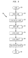
Turning now to FIGURE 3, illustrated is an embodiment
of a method 300 that is carried out according to the
principles of the present invention. The method 300
provides a convenient method to assemble an electronic
device that combines the favorable heat transfer
characteristics of a thermally conductive insert with the
heat transfer characteristics of a polymer potting
material, which are generally inferior to the thermally
conductive inserts.
The method 300 commences in a "start" step 310. In a
"provide case" step 320, a case that is to at least
partially surround the electronic circuit is provided.
In a "place initial layer" step 330, an initial layer of
potting material is located within the case. In one
embodiment of the invention, the initial layer of potting
material has a thickness of about 2 to 6 millimeters. In
a "quick cure" step 340, the initial layer of potting
material is quick-cured (typically by conventional
techniques, such as an ultraviolet or microwave process).
Of course, other methods of quick-curing the potting
material is well within the broad scope of the present
invention. In a "locate insert" step 350, a thermally
conductive insert is located within the case. The
thermally conductive insert may be precut from a sheet of
material with a coefficient of thermal conductivity
greater than the potting material. Alternatively, the
thermally conductive insert may be premolded. In an
advantageous embodiment, the thermally conductive insert
may be located in the case by a machine, such as a pick
and place machine. In a "locate circuit" step 360, the
electronic circuit (having heat generating components
thereon) is placed in the case so that the heat-generating
components can be located proximate the thermally
conductive insert. In a "place potting material" step
370, polymer potting material with a lower coefficient of
thermally conductivity than the thermally conductive
insert is placed within the case to encapsulate both the
electronic circuit and the insert. The method 300
concludes in an send" step 380.
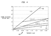
Turning to FIGURE 4, illustrated is a chart plotting
thermal resistance per unit area as a function of
thickness for combinations of materials having different
coefficients of thermal resistance. The thermal
resistance of regular polymer potting material is
indicated by a line 430. The result of combining regular
potting material with thermally conductive inserts having
higher coefficients of thermal conductivity is indicated
by respective lines 410, 420.
Although the present invention has been described in
detail, those skilled in the pertinent art should
understand that they can make various changes,
substitutions and alterations herein without departing
from the spirit and scope of the invention in its broadest
form.