EP1122982A1 - Heating apparatus - Google Patents
Heating apparatus Download PDFInfo
- Publication number
- EP1122982A1 EP1122982A1 EP01300946A EP01300946A EP1122982A1 EP 1122982 A1 EP1122982 A1 EP 1122982A1 EP 01300946 A EP01300946 A EP 01300946A EP 01300946 A EP01300946 A EP 01300946A EP 1122982 A1 EP1122982 A1 EP 1122982A1
- Authority
- EP
- European Patent Office
- Prior art keywords
- heating
- resistance
- heating elements
- terminals
- substrate
- Prior art date
- Legal status (The legal status is an assumption and is not a legal conclusion. Google has not performed a legal analysis and makes no representation as to the accuracy of the status listed.)
- Granted
Links
Images

Classifications
-
- H—ELECTRICITY
- H05—ELECTRIC TECHNIQUES NOT OTHERWISE PROVIDED FOR
- H05B—ELECTRIC HEATING; ELECTRIC LIGHT SOURCES NOT OTHERWISE PROVIDED FOR; CIRCUIT ARRANGEMENTS FOR ELECTRIC LIGHT SOURCES, IN GENERAL
- H05B1/00—Details of electric heating devices
- H05B1/02—Automatic switching arrangements specially adapted to apparatus ; Control of heating devices
- H05B1/0227—Applications
- H05B1/023—Industrial applications
- H05B1/0233—Industrial applications for semiconductors manufacturing
-
- H—ELECTRICITY
- H05—ELECTRIC TECHNIQUES NOT OTHERWISE PROVIDED FOR
- H05B—ELECTRIC HEATING; ELECTRIC LIGHT SOURCES NOT OTHERWISE PROVIDED FOR; CIRCUIT ARRANGEMENTS FOR ELECTRIC LIGHT SOURCES, IN GENERAL
- H05B3/00—Ohmic-resistance heating
-
- H—ELECTRICITY
- H05—ELECTRIC TECHNIQUES NOT OTHERWISE PROVIDED FOR
- H05B—ELECTRIC HEATING; ELECTRIC LIGHT SOURCES NOT OTHERWISE PROVIDED FOR; CIRCUIT ARRANGEMENTS FOR ELECTRIC LIGHT SOURCES, IN GENERAL
- H05B3/00—Ohmic-resistance heating
- H05B3/10—Heating elements characterised by the composition or nature of the materials or by the arrangement of the conductor
- H05B3/12—Heating elements characterised by the composition or nature of the materials or by the arrangement of the conductor characterised by the composition or nature of the conductive material
- H05B3/14—Heating elements characterised by the composition or nature of the materials or by the arrangement of the conductor characterised by the composition or nature of the conductive material the material being non-metallic
- H05B3/141—Conductive ceramics, e.g. metal oxides, metal carbides, barium titanate, ferrites, zirconia, vitrous compounds
- H05B3/143—Conductive ceramics, e.g. metal oxides, metal carbides, barium titanate, ferrites, zirconia, vitrous compounds applied to semiconductors, e.g. wafers heating
-
- H—ELECTRICITY
- H05—ELECTRIC TECHNIQUES NOT OTHERWISE PROVIDED FOR
- H05B—ELECTRIC HEATING; ELECTRIC LIGHT SOURCES NOT OTHERWISE PROVIDED FOR; CIRCUIT ARRANGEMENTS FOR ELECTRIC LIGHT SOURCES, IN GENERAL
- H05B3/00—Ohmic-resistance heating
- H05B3/20—Heating elements having extended surface area substantially in a two-dimensional [2D] plane, e.g. plate-heater
- H05B3/22—Heating elements having extended surface area substantially in a two-dimensional [2D] plane, e.g. plate-heater non-flexible
- H05B3/28—Heating elements having extended surface area substantially in a two-dimensional [2D] plane, e.g. plate-heater non-flexible heating conductor embedded in insulating material
- H05B3/283—Heating elements having extended surface area substantially in a two-dimensional [2D] plane, e.g. plate-heater non-flexible heating conductor embedded in insulating material the insulating material being an inorganic material, e.g. ceramic
-
- H—ELECTRICITY
- H10—SEMICONDUCTOR DEVICES; ELECTRIC SOLID-STATE DEVICES NOT OTHERWISE PROVIDED FOR
- H10P—GENERIC PROCESSES OR APPARATUS FOR THE MANUFACTURE OR TREATMENT OF DEVICES COVERED BY CLASS H10
- H10P72/00—Handling or holding of wafers, substrates or devices during manufacture or treatment thereof
- H10P72/04—Apparatus for manufacture or treatment
- H10P72/0431—Apparatus for thermal treatment
- H10P72/0432—Apparatus for thermal treatment mainly by conduction
Landscapes
- Engineering & Computer Science (AREA)
- Chemical & Material Sciences (AREA)
- Ceramic Engineering (AREA)
- Manufacturing & Machinery (AREA)
- Inorganic Chemistry (AREA)
- Resistance Heating (AREA)
- Surface Heating Bodies (AREA)
Abstract
Description
- The invention relates to a heating apparatus using a ceramic heater.
- The semiconductor-producing apparatus is equipped with a ceramic heater to heat wafers, which are substrates, for manufacturing semiconductor films from raw material gases such as silane gas by thermal CVD or the like.
- The configuration so-called a dual zone heater is known as a ceramic heater. For the dual zone heater, an inner resistance-heating element and an outer resistance-heating element comprising a high-melting point metal such as molybdenum are buried in a ceramic substrate. Separate current-introducing terminals are connected to the respective resistance-heating elements, and the inner resistance-heating element and the outer heating element are independently controlled by applying a predetermined voltage to each resistance-heating element.
- Further, JP-5-326112,A discloses that resistance-heating elements of a ceramic heater are constituted of circuit patterns comprising a plurality of high-melting point metals or the like, wherein the circuit patterns are arranged to compensate their deficient areas with each other. Specifically, one circuit pattern overlaps the deficient areas such as fold or turnover portion of other circuit pattern.
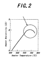
- Particularly for an application to heating semiconductor wafers, controlling the temperature throughout the heating surface uniformly is necessary, and satisfying strict specifications such as temperature differences being within ±5°C throughout the heating surface under a use condition is required. A ceramic heater of dual zone controlling system can usually satisfy such specifications. However, the inventors further studied and found that even the ceramic heater, which kept the temperature uniformly within a range from room temperature to 500°C throughout the heating surface, suddenly caused large temperature differences on the heating surface in a temperature range of, for example, 600°C or higher. In such a case, heat spots usually occurred at particular parts on a peripheral portion of a substrate of the heater. At the same time, the resistance of the whole length of the resistance heater element tended to decrease, rather than to increase, as shown in, for example, FIG. 2.
- It is an object of the invention to prevent increase of the temperature difference on the heating surfaces and occurrence of heat spots in a broad temperature range including a high temperature region in a heating apparatus comprising a substrate made of a ceramic material with a heating surface, a plurality of resistance-heating elements buried in said substance, pairs of terminals, each pair of the terminals being attached to a respective one of the resistance-heating elements to supply alternating current there to, AC power sources each connected to respective one of said pairs of the terminals for the respective resistance-heating elements to supply the alternating current thereto.
- FIG. 1 is a schematic view of a heating apparatus according to an embodiment of the invention.
- FIG. 2 is a graph, showing changes in resistance of a resistance-
heating element 4 when the average temperature of a heating surface was varied within a range of about 400 - 750°C. - FIG. 3 is a measured result of the thermal distribution of a heating surface of a heating apparatus according to Comparative Example as measured by a thermoviewer.
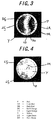
- FIG. 4 is a measured result of the thermal distribution of a heating surface of a heating apparatus according to Invention Example as measured by a thermoviewer.
- The present invention relates to a heating apparatus comprising a substrate made of a ceramic material with a heating surface, a plurality of resistance-heating elements buried in said substrate, pairs of terminals, each pair of the terminals being attached to a respective one of the resistance-heating elements to supply alternating current thereto, AC power sources each connected to a respective one of said pairs of the terminals for the respective resistance-heating elements to supply the alternating current thereto, and insulating transformers each interposed between the respective AC power source and the pair of the terminals.
- The inventors investigated the cause of increased temperature variations and occurrence of heat spots on the heating surfaces of such a heating apparatus in a high temperature range. Firstly, from the observation of the heat spots (as shown in FIG. 3, for example), the inventors considered that two-dimensional pattern of the heat spots might possibly have occurred along a direction (a circumferential direction) in which the resistance-heating elements were buried. Further, the inventors noticed that the resistance (whole-length resistance) of the resistance-heating element tended to decrease in the high temperature range as shown in FIG. 2. Since the volume resistivity of a metal generally increases along with temperature rise, the resistance decrease shown in FIG. 2 is considered to be caused not by the change of the material etc. of the resistance-heating element, but by the ceramics.
- In the view of this, the inventors further investigated to reach an idea that a leakage current flow through the ceramics between adjacent regions of each resistance-heating elements when the temperature excess a certain level. Especially in the case of the ceramics having a negative thermal coefficient, the leakage current can easily flow. When the leakage current flows, the current in the resistance-heating element increases locally to rise the heat generation, thus the leakage current tends to be further increased more. It is considered that the leakage current is amplified to generate the heat spots in such a process.
- Based on this assumption, insulating transformers are each interposed between the resistance-heating element and the power source, to isolate the current flowing one resistance-heating element from that flowing the other. That is, the insulating transformers are independently constitutes closed circuits, so that the current flowing one insulating transformer flows the corresponding closed circuit, but does not leaks therefrom or receive a leak current from other circuit unlike an open circuit. As the result, the heat spots are nearly solved and the temperature differences on the heating surface is remarkably reduced, for example, as shown in FIG. 4.
- Although the kinds of ceramics are not limited, aluminum nitride, silicon nitride and boron nitride are preferably used in the view of the temperature coefficient of the volume resistivity being negative and its absolute value being large, and aluminum nitride is more preferably used in the view of corrosion resistance.
- The invention is particularly useful when the temperature coefficient of the volume resistivity of the material of the resistance-heating element is positive. Preferably, high-melting point metals such as tantalum, tungsten, molybdenum, platinum, rhenium, hafnium and alloys thereof are used as specific materials of the resistance-heating element. Especially, when the ceramic substrate is composed of aluminum nitride, molybdenum and a molybdenum alloy are preferably used. Conductive materials such as carbon, TiN and TiC can be also used other besides high-melting point metals.
- The resistance-heating elements preferably comprise a plurality of planar resistance-heating elements provided in the form of layers as viewed in a thickness direction of the substrate, wherein each planar resistance-heating elements have heat-generating density increased portions in mutually different locations or in a partially overlapped relation as viewed in a plane. More preferably, the planar resistance-heating elements are arranged in nearly parallel to the heating surface of the substrate. These embodiments will be explained in more detail with reference to FIG. 1.
- FIG. 1 is a schematic view of a heating apparatus according to an embodiment of the invention. For the expedience of an explanation, the details of the apparatus are simplified and sizes of each part of the apparatus are drawn with a scale different from those of the actual heating apparatus.
- A ceramic heater 1 comprises a
substrate 2, an upper planar resistance-heating element 3 and a lower planar resistance-heating element 4 both of which are buried in thesubstrate 2. Current-introducingterminals substrate 2. - The resistance-
heating elements heating surface 2A of thesubstrate 2. The upper planar resistance-heating element 3 has a heat-generating density increasedportion 3A in an outer peripheral region of thesubstrate 2, and the lower planar resistance-heating element 4 has a heat-generating density increasedportion 4A in an inner region of thesubstrate 2. - One ends of the
terminals 5 are connected to the upper planar resistance-heating element 3, and one ends of theterminals 6 connected to the heat-generating density increasedportion 4A of the lower planar resistance-heating element 4. The terminals were 4 mm in diameter and 15 mm in length, consisted of Ni and had KOVAR heads which were connected with an Au-Ni brazing material.Lead wires terminals lead wires 9 are connected to anAC power source 11A via aninsulating transformer 10A. Thelead wires 8 are connected to anAC power source 11B via aninsulating transformer 10B. Electric power supplied by eachAC power source - A
cylindrical member 7 is joined on the rear side of thesubstrate 2, which protects the other ends of the current-introducingterminals substrate 2. - When the resistance of the ceramics decreases in the high temperature region, a leakage current flows, for example, between the heat-generating density increased
portion 3A and theheating element 4 to cause a heat spot. The invention can prevent such a leakage current between the resistance-heating elements in the respective layers. - Moreover, the following functions and effects can be acquired by the heating apparatus as shown in FIG. 1. For example, when such a dual zone ceramic heater as shown in FIG. 1 has been operated for a long period, the substrate and each resistance-heating element are frequently heated and cooled. By such heating-cooling cycles, the current-introducing terminals connected to the resistance-heating elements undergo shear stress resulting from the difference in thermal expansion, which is based on difference in the coefficient of thermal expansion between the ceramic constituting the substrate and the high-melting point metal constituting the resistance-heating elements. When such shear stress frequently applies on the terminals, the terminals may be broken by fatigue fracture.
- Generally, the resistance-heating elements are joined to the current-introducing terminals by a brazing material. The brazed junction may be possibly broken away by a shear stress resulting from the difference in thermal expansion between the resistance-heating element and the brazing filler metal.
- If the current-introducing terminal is separated from a resistance-heating element, no current supplies to the resistance-heating element, thus no heat is generated. Therefore, a large temperature difference may occur in the ceramic substrate to cause cracks in the ceramics.
- On the other hand, according to such a heating apparatus as shown in FIG. 1, for example, the planar resistance-heating elements have heat-generating density increased portions in mutually different locations (locations without overlapping) as viewed in a plane, although the heat-generating density increased portions can also be partially overlapped as viewed in a plane. Herewith, the apparatus can perform as a dual zone heater without any problems. The reason is that the supplied power to the resistance-
heating element 4 can be increased to enlarge the contribution of the heat-generating density increasedportion 4A when the temperature of the inner circumferential side is needed to rise. Further, the supplied power to the resistance-heating element 3 can be increased to enlarge the contribution of the heat-generating density increasedportion 3A when the temperature of the outer circumferential side is needed to rise. - At the same time, for example, when the upper planar resistance-
heating element 3 stops generating heat, only the lower planar resistance-heating element 4 generates heat. In this case, however, the difference in heating-generated amount between the heat-generating density increasedportion 4A and the other parts is smaller than that of conventional dual zone heaters. Therefore, the temperature difference between the outer circumferential side and the inner circumferential side of the substrate is relatively small, thus cracks are difficult to be initiated. - In the ceramic heater as shown in FIG. 1, the upper planar resistance-
heating element 3 and lower planar resistance-heating element 4 are arranged to be nearly parallel to theheating surface 2A of thesubstrate 2. Thereby, vertical heat conduction in theceramic substrate 2 is performed quite uniformly. Therefore, when an object to be heated, a semiconductor wafer, for example, is laid on theheating surface 2A, the wafer can be heated uniformly and efficiently. Note that "nearly parallel" herein is within a range from -0.5 degree to 0.5 degree, in addition to "geometrically completely parallel." - Moreover, in the ceramic heater according to the invention, when each planar resistance-heating element is heated, temperature variations of the heating surface of the substrate are preferably within 50°C, more preferably within 20°C. Thereby, for example, even when the electric current stops flowing into the upper planar resistance-
heating element 3 in FIG. 1 and the upper planar resistance-heating element stops acting as a heating element, since well uniform heating can be achieved by the lower planar resistance-heating element 4 alone, cracks that would be caused by uneven temperature distribution in the substrate can be effectively restrained. Further, the object to be heated on theheating surface 2A can be heated more uniformly. - The shape of the resistance-heating element of the heating apparatus according to the invention is not limited, as far as the object of the invention can be achieved. For example, the resistance-heating element may be constituted from a network member, a coilspring, and a ribbon member or the like. For giving a remarkable resistance to the heating-cooling thermal cycles on operating the ceramic heater, the resistance-heating element may be preferably constituted from the network member or coilspring. Moreover, a planar shape of the resistance-heating element is not particularly limited.
- When the planar resistance-heating element is constituted from a network member, the heat density increasing area is formed either by weaving the net in a prescribed part at a high density or by reducing the cross section of a prescribed part of the material constituting the network member. When the planar resistance-heating element is constituted from a coilspring, the heat-generating density increased portion is formed either by increasing the number of turns or pitch at a prescribed part or by enlarging the diameter of concentric turns constituting the coil at a prescribed part. When the planar resistance-heating element is constituted from a ribbon member, the heat-generating density increased portion is formed by reducing the width of the ribbon at a prescribed part.
- A heating apparatus as schematically shown in FIG. 1 was prepared. Specifically, aluminum nitride powder obtained from the reduction nitriding method was used, acrylic binder was added to the powder, and the mixture was granulated by a spray dryer, thereby obtaining the granulated grains. Three molded sheet were sequentially uniaxially press-molded, thereby laminating and integrating them. Coil-shaped resistance-
heating elements - The molded body was placed in a hot press mold, which was hermetically sealed. The molded body was heated at a heating rate of 300°C/hour, while the pressure was reduced in a temperature range from the room temperature to 1,000°C. Then, the pressure was increased simultaneously with increase in temperature. The maximum temperature was 1,800°C, and the molded body was held and fired at the maximum temperature under 200 kgf/cm2 for 4 hours in nitrogen gas to obtain a sintered body. Then the sintered body was subjected to a machine work and a finish machining, thereby a heater was prepared. The diameter and the thickness of a
substrate 2 were set to 240 mm and 18 mm, respectively, and the thickness of an insulative conductive layer was set to 1 mm. The clearance between the resistance-heating elements - A circuit was formed as schematically shown in FIG. 1 in Invention Example. In Comparative Example, insulating
transformers wires AC power sources - By controlling power supply from each AC power source, the average temperature of the heating surface of the heating apparatus was varied from about 400 to 700°C to measure temperature changes in resistance between a pair of
terminals 6 of the resistance-heating element 4. A result is shown in FIG. 2. - Moreover, surface temperature distribution of the heating surface at the average temperature of the heating surface being 700°C was measured by a themoviewer. A measurement result of Comparative Example is shown in FIG. 3 and a measurement result of Invention Example is shown in FIG. 4. In FIGS. 3 and 4, a warm color region represents a high temperature and a cold color region represents a low temperature. For example, the temperature decreases from red to yellow, green and blue, and a step of color tone corresponds to 2.5°C. In other words, a temperature difference of 2.5°C corresponds to a change between two adjacent color regions in different tones of a step. Therefore, from the results observed by the thermoviewer, the difference between the highest and the lowest temperatures of the heating surface can be calculated. The calculated result is 26°C in Comparative Example, and 7.5°C in Invention Example.
- As mentioned above, according to the invention, increased temperature differences and heat spots on the heating surfaces of the said heating apparatus can be prevented over a broad temperature range including the high temperature region.
Claims (7)
- A heating apparatus comprising substrate made of a ceramic material with a heating surface, a plurality of resistance-heating elements buried in said substrate, pairs of terminals, each pair of the terminals being attached to a respective one of the resistance-heating elements to supply alternating current thereto, AC power sources each connected to a respective one of said pairs of terminals for the respective resistance-heating elements to supply the alternating current thereto, and insulating transformers each interposed between the AC power sources and pair of the terminals.
- A heating apparatus according to claim 1, wherein the temperature coefficient of a volume resistivity of said ceramic material is negative.
- A heating apparatus according to claim 2, wherein said ceramic comprises aluminum nitride.
- A heating apparatus according to claims 2 or 3, wherein the temperature coefficient of a volume resistivity of a material constituting said resistance-heating elements is positive.
- A heating apparatus according to any one of claims 1 to 4, wherein said resistance-heating elements comprise a plurality of planar resistance-heating elements provided in the form of layers as viewed in a thickness direction, said planar resistance-heating elements having respective heat-generating density increased portions in mutually different locations or in a partially overlapped relation as viewed in a plane.
- A heating apparatus according to claim 5, wherein said planar resistance-heating elements are arranged in nearly parallel to said heating surface of said substrate.
- A heating apparatus according to claim 5 or 6, wherein temperature variations of said heating surface is within 50°C when the alternative power is supplied only to any one of a plurality of said planar resistance-heating elements for heating.
Applications Claiming Priority (2)
| Application Number | Priority Date | Filing Date | Title |
|---|---|---|---|
| JP2000026582 | 2000-02-03 | ||
| JP2000026582A JP4028149B2 (en) | 2000-02-03 | 2000-02-03 | Heating device |
Publications (2)
| Publication Number | Publication Date |
|---|---|
| EP1122982A1 true EP1122982A1 (en) | 2001-08-08 |
| EP1122982B1 EP1122982B1 (en) | 2003-05-02 |
Family
ID=18552299
Family Applications (1)
| Application Number | Title | Priority Date | Filing Date |
|---|---|---|---|
| EP01300946A Expired - Lifetime EP1122982B1 (en) | 2000-02-03 | 2001-02-02 | Heating apparatus |
Country Status (6)
| Country | Link |
|---|---|
| US (1) | US6376811B2 (en) |
| EP (1) | EP1122982B1 (en) |
| JP (1) | JP4028149B2 (en) |
| KR (1) | KR100407052B1 (en) |
| DE (1) | DE60100216T2 (en) |
| TW (1) | TW472498B (en) |
Families Citing this family (28)
| Publication number | Priority date | Publication date | Assignee | Title |
|---|---|---|---|---|
| JP3293594B2 (en) * | 1999-06-29 | 2002-06-17 | 住友電気工業株式会社 | Apparatus and method for heating protective member of optical fiber fusion spliced part |
| ATE301916T1 (en) * | 1999-11-19 | 2005-08-15 | Ibiden Co Ltd | CERAMIC HEATER |
| CN1299322C (en) * | 2000-11-16 | 2007-02-07 | 麦特逊技术股份有限公司 | Apparatuses and methods for resistively heating thermal processing system |
| JP2004253665A (en) * | 2003-02-21 | 2004-09-09 | Sumitomo Electric Ind Ltd | Wafer holder for semiconductor manufacturing apparatus and semiconductor manufacturing apparatus equipped with the same |
| JP2004296254A (en) * | 2003-03-27 | 2004-10-21 | Sumitomo Electric Ind Ltd | Ceramic heater and semiconductor or liquid crystal manufacturing apparatus equipped with the same |
| US20040222210A1 (en) * | 2003-05-08 | 2004-11-11 | Hongy Lin | Multi-zone ceramic heating system and method of manufacture thereof |
| US7126092B2 (en) * | 2005-01-13 | 2006-10-24 | Watlow Electric Manufacturing Company | Heater for wafer processing and methods of operating and manufacturing the same |
| US8168926B2 (en) * | 2007-03-26 | 2012-05-01 | Ngk Insulators, Ltd. | Heating device |
| NZ598371A (en) * | 2007-07-31 | 2013-08-30 | Resmed Ltd | Heating element, humidifier for respiratory apparatus including heating element and respiratory apparatus |
| US8193473B2 (en) * | 2008-02-08 | 2012-06-05 | Ngk Insulators, Ltd. | Uniform temperature heater |
| KR101433865B1 (en) * | 2008-02-25 | 2014-08-29 | 주성엔지니어링(주) | A substrate processing apparatus having a fixed lift pin and a method of loading and unloading a substrate using the same |
| US20100108661A1 (en) * | 2008-10-31 | 2010-05-06 | United Technologies Corporation | Multi-layer heating assembly and method |
| CN102280366B (en) * | 2011-08-19 | 2014-01-01 | 清华大学 | Rotating window piece apparatus used for laser processing |
| WO2013130918A1 (en) | 2012-02-29 | 2013-09-06 | Harris, Jonathan, H. | Transient liquid phase, pressureless joining of aluminum nitride components |
| JP6077258B2 (en) * | 2012-10-05 | 2017-02-08 | 日本特殊陶業株式会社 | Laminate heating element, electrostatic chuck, and ceramic heater |
| JP6690918B2 (en) * | 2015-10-16 | 2020-04-28 | 日本特殊陶業株式会社 | Heating member, electrostatic chuck, and ceramic heater |
| US20170140956A1 (en) * | 2015-11-13 | 2017-05-18 | Varian Semiconductor Equipment Associates, Inc. | Single Piece Ceramic Platen |
| JP6806768B2 (en) * | 2016-04-28 | 2021-01-06 | 京セラ株式会社 | Heater system, ceramic heater, plasma processing device and adsorption device |
| JP6758143B2 (en) * | 2016-09-29 | 2020-09-23 | 日本特殊陶業株式会社 | Heating device |
| US10679873B2 (en) * | 2016-09-30 | 2020-06-09 | Ngk Spark Plug Co., Ltd. | Ceramic heater |
| US11289355B2 (en) * | 2017-06-02 | 2022-03-29 | Lam Research Corporation | Electrostatic chuck for use in semiconductor processing |
| US11469084B2 (en) | 2017-09-05 | 2022-10-11 | Lam Research Corporation | High temperature RF connection with integral thermal choke |
| US11382180B2 (en) * | 2017-11-21 | 2022-07-05 | Watlow Electric Manufacturing Company | Multi-zone pedestal heater having a routing layer |
| CN111670491A (en) | 2018-01-31 | 2020-09-15 | 朗姆研究公司 | Electrostatic Chuck (ESC) Base Voltage Isolation |
| US11086233B2 (en) | 2018-03-20 | 2021-08-10 | Lam Research Corporation | Protective coating for electrostatic chucks |
| US11183368B2 (en) | 2018-08-02 | 2021-11-23 | Lam Research Corporation | RF tuning systems including tuning circuits having impedances for setting and adjusting parameters of electrodes in electrostatic chucks |
| CN113170539B (en) * | 2019-01-25 | 2023-03-14 | 日本碍子株式会社 | ceramic heater |
| GB2605626B (en) * | 2021-04-08 | 2024-10-02 | Dyson Technology Ltd | A heater |
Citations (3)
| Publication number | Priority date | Publication date | Assignee | Title |
|---|---|---|---|---|
| US5225663A (en) * | 1988-06-15 | 1993-07-06 | Tel Kyushu Limited | Heat process device |
| US5331134A (en) * | 1992-05-21 | 1994-07-19 | Shin-Etsu Chemical Co., Ltd. | Double-layered ceramic heater |
| JPH1184939A (en) * | 1997-09-11 | 1999-03-30 | Canon Inc | Image recording device |
Family Cites Families (16)
| Publication number | Priority date | Publication date | Assignee | Title |
|---|---|---|---|---|
| US4449039A (en) * | 1981-09-14 | 1984-05-15 | Nippondenso Co., Ltd. | Ceramic heater |
| JPS61109289A (en) * | 1984-11-01 | 1986-05-27 | 日本碍子株式会社 | Ceramic heater and manufacture thereof |
| US4912304A (en) * | 1987-09-09 | 1990-03-27 | Philippbar Jay E | Thick-film incubator |
| US5408574A (en) * | 1989-12-01 | 1995-04-18 | Philip Morris Incorporated | Flat ceramic heater having discrete heating zones |
| DE69111493T2 (en) * | 1990-03-12 | 1996-03-21 | Ngk Insulators Ltd | Wafer heaters for apparatus, for semiconductor manufacturing heating system with these heaters and manufacture of heaters. |
| DE4240812A1 (en) * | 1992-12-04 | 1994-06-09 | Bosch Gmbh Robert | Heater arrangement for a sensor for determining components in gases |
| JP3228581B2 (en) * | 1992-12-24 | 2001-11-12 | 京セラ株式会社 | Ceramic heater |
| JPH06202512A (en) * | 1992-12-29 | 1994-07-22 | Canon Inc | Heating device and image recorder |
| JP2642858B2 (en) * | 1993-12-20 | 1997-08-20 | 日本碍子株式会社 | Ceramic heater and heating device |
| JP2813148B2 (en) * | 1994-03-02 | 1998-10-22 | 日本碍子株式会社 | Ceramic products |
| US6002109A (en) * | 1995-07-10 | 1999-12-14 | Mattson Technology, Inc. | System and method for thermal processing of a semiconductor substrate |
| US5940579A (en) * | 1997-02-26 | 1999-08-17 | White Consolidated Industries, Inc. | Capacitive leakage current cancellation for heating panel |
| JP3318514B2 (en) * | 1997-08-06 | 2002-08-26 | 日本碍子株式会社 | Semiconductor support device |
| JP3691649B2 (en) * | 1997-10-28 | 2005-09-07 | 日本特殊陶業株式会社 | Ceramic heater |
| JPH11204238A (en) * | 1998-01-08 | 1999-07-30 | Ngk Insulators Ltd | Ceramic heater |
| JPH11260534A (en) * | 1998-01-09 | 1999-09-24 | Ngk Insulators Ltd | Heating device and method of manufacturing the same |
-
2000
- 2000-02-03 JP JP2000026582A patent/JP4028149B2/en not_active Expired - Lifetime
- 2000-12-16 TW TW089126966A patent/TW472498B/en not_active IP Right Cessation
-
2001
- 2001-01-31 US US09/773,235 patent/US6376811B2/en not_active Expired - Lifetime
- 2001-02-01 KR KR10-2001-0004793A patent/KR100407052B1/en not_active Expired - Lifetime
- 2001-02-02 EP EP01300946A patent/EP1122982B1/en not_active Expired - Lifetime
- 2001-02-02 DE DE60100216T patent/DE60100216T2/en not_active Expired - Lifetime
Patent Citations (3)
| Publication number | Priority date | Publication date | Assignee | Title |
|---|---|---|---|---|
| US5225663A (en) * | 1988-06-15 | 1993-07-06 | Tel Kyushu Limited | Heat process device |
| US5331134A (en) * | 1992-05-21 | 1994-07-19 | Shin-Etsu Chemical Co., Ltd. | Double-layered ceramic heater |
| JPH1184939A (en) * | 1997-09-11 | 1999-03-30 | Canon Inc | Image recording device |
Non-Patent Citations (1)
| Title |
|---|
| PATENT ABSTRACTS OF JAPAN vol. 1999, no. 08 30 June 1999 (1999-06-30) * |
Also Published As
| Publication number | Publication date |
|---|---|
| KR20010078235A (en) | 2001-08-20 |
| KR100407052B1 (en) | 2003-11-28 |
| JP4028149B2 (en) | 2007-12-26 |
| US6376811B2 (en) | 2002-04-23 |
| DE60100216T2 (en) | 2004-03-18 |
| DE60100216D1 (en) | 2003-06-05 |
| TW472498B (en) | 2002-01-11 |
| US20010027972A1 (en) | 2001-10-11 |
| EP1122982B1 (en) | 2003-05-02 |
| JP2001217059A (en) | 2001-08-10 |
Similar Documents
| Publication | Publication Date | Title |
|---|---|---|
| EP1122982B1 (en) | Heating apparatus | |
| US7126092B2 (en) | Heater for wafer processing and methods of operating and manufacturing the same | |
| US7173219B2 (en) | Ceramic heaters | |
| KR100495987B1 (en) | A heating system | |
| JP3897563B2 (en) | Heating device | |
| EP1089593A2 (en) | Ceramic heater | |
| KR20200120720A (en) | Multi zone heater | |
| US20020102512A1 (en) | Ceramic heater | |
| CN108738173B (en) | Ceramic component | |
| EP1621048B1 (en) | Multi-zone ceramic heating system and method of manufacture thereof | |
| US6946625B2 (en) | Ceramic susceptor | |
| JP2018182280A (en) | Ceramic member | |
| US7332694B2 (en) | Heating resistances and heaters | |
| TW200527580A (en) | Heating device | |
| US7115839B2 (en) | Heaters | |
| US20050184054A1 (en) | Ceramics heater for semiconductor production system | |
| JPH11162620A (en) | Ceramic heater and method of soaking | |
| US7394043B2 (en) | Ceramic susceptor | |
| US7157666B2 (en) | Systems for producing semiconductors and members therefor | |
| JP4671262B2 (en) | Semiconductor heating device | |
| JPH1154245A (en) | Ceramic heater | |
| JP6711738B2 (en) | Support device | |
| JP2006286646A (en) | Ceramic heater |
Legal Events
| Date | Code | Title | Description |
|---|---|---|---|
| PUAI | Public reference made under article 153(3) epc to a published international application that has entered the european phase |
Free format text: ORIGINAL CODE: 0009012 |
|
| AK | Designated contracting states |
Kind code of ref document: A1 Designated state(s): DE FR GB |
|
| AX | Request for extension of the european patent |
Free format text: AL;LT;LV;MK;RO;SI |
|
| 17P | Request for examination filed |
Effective date: 20020131 |
|
| AKX | Designation fees paid |
Free format text: DE FR GB |
|
| 17Q | First examination report despatched |
Effective date: 20020424 |
|
| GRAH | Despatch of communication of intention to grant a patent |
Free format text: ORIGINAL CODE: EPIDOS IGRA |
|
| GRAH | Despatch of communication of intention to grant a patent |
Free format text: ORIGINAL CODE: EPIDOS IGRA |
|
| GRAA | (expected) grant |
Free format text: ORIGINAL CODE: 0009210 |
|
| AK | Designated contracting states |
Designated state(s): DE FR GB |
|
| REG | Reference to a national code |
Ref country code: GB Ref legal event code: FG4D |
|
| REF | Corresponds to: |
Ref document number: 60100216 Country of ref document: DE Date of ref document: 20030605 Kind code of ref document: P |
|
| ET | Fr: translation filed | ||
| PLBE | No opposition filed within time limit |
Free format text: ORIGINAL CODE: 0009261 |
|
| STAA | Information on the status of an ep patent application or granted ep patent |
Free format text: STATUS: NO OPPOSITION FILED WITHIN TIME LIMIT |
|
| 26N | No opposition filed |
Effective date: 20040203 |
|
| REG | Reference to a national code |
Ref country code: FR Ref legal event code: PLFP Year of fee payment: 16 |
|
| REG | Reference to a national code |
Ref country code: FR Ref legal event code: PLFP Year of fee payment: 17 |
|
| REG | Reference to a national code |
Ref country code: FR Ref legal event code: PLFP Year of fee payment: 18 |
|
| PGFP | Annual fee paid to national office [announced via postgrant information from national office to epo] |
Ref country code: GB Payment date: 20200122 Year of fee payment: 20 Ref country code: DE Payment date: 20200121 Year of fee payment: 20 |
|
| PGFP | Annual fee paid to national office [announced via postgrant information from national office to epo] |
Ref country code: FR Payment date: 20200113 Year of fee payment: 20 |
|
| REG | Reference to a national code |
Ref country code: DE Ref legal event code: R071 Ref document number: 60100216 Country of ref document: DE |
|
| REG | Reference to a national code |
Ref country code: GB Ref legal event code: PE20 Expiry date: 20210201 |
|
| PG25 | Lapsed in a contracting state [announced via postgrant information from national office to epo] |
Ref country code: GB Free format text: LAPSE BECAUSE OF EXPIRATION OF PROTECTION Effective date: 20210201 |