EP1122807A1 - Dielectric resonator and dielectric filter - Google Patents
Dielectric resonator and dielectric filter Download PDFInfo
- Publication number
- EP1122807A1 EP1122807A1 EP00953537A EP00953537A EP1122807A1 EP 1122807 A1 EP1122807 A1 EP 1122807A1 EP 00953537 A EP00953537 A EP 00953537A EP 00953537 A EP00953537 A EP 00953537A EP 1122807 A1 EP1122807 A1 EP 1122807A1
- Authority
- EP
- European Patent Office
- Prior art keywords
- dielectric
- resonator
- filter
- degrees
- dielectric resonator
- Prior art date
- Legal status (The legal status is an assumption and is not a legal conclusion. Google has not performed a legal analysis and makes no representation as to the accuracy of the status listed.)
- Granted
Links
- 239000000523 sample Substances 0.000 claims abstract description 41
- 230000008878 coupling Effects 0.000 claims description 31
- 238000010168 coupling process Methods 0.000 claims description 31
- 238000005859 coupling reaction Methods 0.000 claims description 31
- 241000217377 Amblema plicata Species 0.000 claims description 20
- 229910052751 metal Inorganic materials 0.000 claims description 16
- 239000002184 metal Substances 0.000 claims description 16
- 238000005192 partition Methods 0.000 claims description 10
- 239000004020 conductor Substances 0.000 claims description 3
- 238000010586 diagram Methods 0.000 description 52
- 239000003989 dielectric material Substances 0.000 description 20
- 230000000052 comparative effect Effects 0.000 description 12
- 230000005684 electric field Effects 0.000 description 9
- 238000005549 size reduction Methods 0.000 description 9
- 238000000034 method Methods 0.000 description 7
- 230000009977 dual effect Effects 0.000 description 5
- 230000000694 effects Effects 0.000 description 5
- 230000005284 excitation Effects 0.000 description 5
- 238000004519 manufacturing process Methods 0.000 description 5
- 238000003780 insertion Methods 0.000 description 3
- 230000037431 insertion Effects 0.000 description 3
- 239000010949 copper Substances 0.000 description 2
- GWEVSGVZZGPLCZ-UHFFFAOYSA-N titanium dioxide Inorganic materials O=[Ti]=O GWEVSGVZZGPLCZ-UHFFFAOYSA-N 0.000 description 2
- RYGMFSIKBFXOCR-UHFFFAOYSA-N Copper Chemical compound [Cu] RYGMFSIKBFXOCR-UHFFFAOYSA-N 0.000 description 1
- 230000003213 activating effect Effects 0.000 description 1
- 229910052782 aluminium Inorganic materials 0.000 description 1
- XAGFODPZIPBFFR-UHFFFAOYSA-N aluminium Chemical compound [Al] XAGFODPZIPBFFR-UHFFFAOYSA-N 0.000 description 1
- 238000013459 approach Methods 0.000 description 1
- 230000005540 biological transmission Effects 0.000 description 1
- 229910052802 copper Inorganic materials 0.000 description 1
- 230000005672 electromagnetic field Effects 0.000 description 1
- 230000002349 favourable effect Effects 0.000 description 1
- 230000004907 flux Effects 0.000 description 1
- 238000000227 grinding Methods 0.000 description 1
- 230000009931 harmful effect Effects 0.000 description 1
- 239000000463 material Substances 0.000 description 1
- 238000012545 processing Methods 0.000 description 1
- 230000009467 reduction Effects 0.000 description 1
- 230000017105 transposition Effects 0.000 description 1
Images









Classifications
-
- H—ELECTRICITY
- H01—ELECTRIC ELEMENTS
- H01P—WAVEGUIDES; RESONATORS, LINES, OR OTHER DEVICES OF THE WAVEGUIDE TYPE
- H01P1/00—Auxiliary devices
- H01P1/20—Frequency-selective devices, e.g. filters
-
- H—ELECTRICITY
- H01—ELECTRIC ELEMENTS
- H01P—WAVEGUIDES; RESONATORS, LINES, OR OTHER DEVICES OF THE WAVEGUIDE TYPE
- H01P7/00—Resonators of the waveguide type
- H01P7/10—Dielectric resonators
- H01P7/105—Multimode resonators
-
- H—ELECTRICITY
- H01—ELECTRIC ELEMENTS
- H01P—WAVEGUIDES; RESONATORS, LINES, OR OTHER DEVICES OF THE WAVEGUIDE TYPE
- H01P1/00—Auxiliary devices
- H01P1/20—Frequency-selective devices, e.g. filters
- H01P1/207—Hollow waveguide filters
- H01P1/208—Cascaded cavities; Cascaded resonators inside a hollow waveguide structure
- H01P1/2084—Cascaded cavities; Cascaded resonators inside a hollow waveguide structure with dielectric resonators
-
- H—ELECTRICITY
- H01—ELECTRIC ELEMENTS
- H01P—WAVEGUIDES; RESONATORS, LINES, OR OTHER DEVICES OF THE WAVEGUIDE TYPE
- H01P1/00—Auxiliary devices
- H01P1/20—Frequency-selective devices, e.g. filters
- H01P1/207—Hollow waveguide filters
- H01P1/208—Cascaded cavities; Cascaded resonators inside a hollow waveguide structure
- H01P1/2084—Cascaded cavities; Cascaded resonators inside a hollow waveguide structure with dielectric resonators
- H01P1/2086—Cascaded cavities; Cascaded resonators inside a hollow waveguide structure with dielectric resonators multimode
Definitions
- the present invention relates to a dielectric filter used in radio communications, and the like at high frequency band as microwave band, quasi-microwave band, and the like and a dielectric resonator used in the dielectric filter, and more particularly to a triple mode dielectric resonator in which three resonant modes are available in one dielectric block and a dielectric filter using the dielectric resonator therein.
- a dielectric filter which providing a cut-off waveguide with cylindrical or rectangular parallelopiped dielectrics disposing successively therein and utilizing resonance of a cylindrical TE01 ⁇ mode or a rectangular TE11 ⁇ mode of dielectrics is utilized widely in filters requiring low loss and size reduction, because the dielectric filter has high unloaded Q and can be reduced in size easier than waveguide type filter (a first conventional example).
- a resonance of the mode is generated by an electric field repeating reflections at an interface surface of the dielectric resonator and the air.
- the resonant frequency of dielectric resonator is inversely proportional to the length of the resonator and square root of dielectric constant, so that the larger the dielectric constant is, the smaller the resonator is.
- a magnetic field generated by the resonance excites a resonator on the next stage and the excitation corresponds to the coupling between stages of the dielectric filter.
- a magnitude of the coupling is mainly determined by the distance between resonators, the farther the distance is, the weaker the coupling is.
- adjusting means for the above-mentioned dielectric filter a method of adjusting the resonant frequency by a screw in a direction orthogonal to the reflecting surface of the magnetic field or a method of adjusting the coupling between the resonators by a screw, and the like are adoptable.
- dielectric filter utilizing a dual mode dielectric resonator in order to achieve size reduction (a second conventional example).
- the above-mentioned dielectric resonator provides two resonance by one resonator, in which a cylindrical dielectric resonator is disposed in the center of a cylindrical waveguide by justifying the axes of the cylinders, for example, and two resonance (HE11 ⁇ ) generated in two directions orthogonal to the axes of the cylinders are coupled by disturbing the electromagnetic field of the resonance from the waveguide side using means as screws, and the like.
- the resonant frequency of the resonator by a cylindrical TE01 ⁇ mode or a rectangular TE11 ⁇ mode of dielectrics depends on dielectric constant and the size of dielectrics and a resonator can be smaller when the dielectric constant gets larger, accordingly the simplest method of reducing size of the filter utilizing the dielectric resonator is to raise the dielectric constant of dielectrics.
- dielectrics with low dielectric loss used in microwave region generally has a characteristic that dielectric loss thereof increases as dielectric constant becomes higher, size reduction of the filter maintaining insertion loss low has a certain limitation. Further, as dielectrics with low loss as mentioned above is expensive, accordingly the filter becomes expensive when the filter provides more stages, that is, provides more dielectrics used therein.
- a filter relative to a second conventional example utilizing HE11 ⁇ dual mode dielectric resonator for size reduction has a problem that lots of undesired modes excited in the vicinity of pass band result in spurious characteristic deteriorated easily, because HE11 ⁇ is not the dominant mode.
- composing a dielectric filter using dielectric resonators capable of multiple mode resonance is proposed to realize a band pass filter with a very small and simple composition exploiting advantages in using dielectric resonators fully.
- size reduction of a band pass filter having a double-tuned band characteristic by varying the resonant frequency of the two resonance modes to each other is proposed in unexamined Japanese Patent Publication No. Hei 7-58516, in which degenerate coupling of two resonance modes with respect to TE101 and TE01 ⁇ modes is disclosed (a third conventional example).
- a multiple mode dielectric resonator capable of generating TM01 ⁇ mode and TE01 ⁇ mode which are generated on a surface parallel to each surface (x-y surface, y-z surface, x-z surface) in a rectangular coordinate system in a generally rectangular parallelopiped shaped dielectric block is proposed in unexamined Japanese Patent Publication No. Hei 11-145704 (a fourth conventional example).
- a dielectric resonator occupies a large amount of volume in a band pass filter requiring a resonator of multiple stages, even though the degenerate coupling of two resonance modes relative to the above-mentioned third conventional example as described in unexamined Japanese Patent Publication No. Hei 7-58516 is utilized. And even a triple mode dielectric resonator relative to the fourth example as described in unexamined Japanese Patent Publication No. Hei 11-145704 has a problem that the manufacturing process becomes complicated, because utilization of hybrid coupling of TM01 ⁇ mode and TE01 ⁇ mode which are orthogonal spatially requires the thickness of dielectric resonator to be adjusted to resonant frequency.
- a second object of the present invention is to solve the problem of the above-mentioned third and fourth conventional examples and to provide a very small dielectric resonator with simple composition in spite of enabling a triple mode resonance and a dielectric filter using the above-mentioned dielectric resonator.
- the present invention aims at size reduction of dielectric filter by using three resonant modes in one dielectric block in order to achieve a first object of the above-mentioned present invention. That is, in a block of a generally rectangular parallelopiped consisting of dielectric material, three, resonant modes in a single dielectric block can be coupled by chamfering a ridge portion of the dielectric block and another ridge portion unparallel thereto.
- the dielectric resonator claimed in claim 1 is characterized in combining three resonant modes of the above-mentioned dielectric block by removing one ridge portion and another ridge portion unparallel thereto in a block of a generally rectangular parallelopiped.
- a rectangular TE11 ⁇ mode can exist in each of three orthogonal axial direction in a block of a generally rectangular parallelopiped.
- the filter is composed using only one or two resonance out of the above-mentioned resonance of three axial direction, while the rest of the resonance exerts a harmful effect as undesired resonance.
- the rest of the resonance is utilized positively so that one resonator acts as three resonators.
- a dielectric filter claimed in claim 2 is characterized in disposing at least one dielectric resonator claimed in claim 1 in a cut-off waveguide.
- a small dielectric filter with low insertion loss can be manufactured by composing a filter in which one or more of the above-mentioned dielectric resonators are disposed in the cut-off waveguide.
- a dielectric filter claimed in claim 3 is characterized in disposing two or more of the above-mentioned dielectric resonators in the above-mentioned cut-off waveguide and providing means for partition consisting of electric conductive material between the above-mentioned dielectric resonators.
- a dielectric filter claimed in claim 4 is characterized in disposing a metal rod contacting with the above-mentioned waveguide by one end parallel to a side surface of the above-mentioned dielectric resonator in a position away from the above-mentioned side surface by a predetermined distance, in which resonant frequency of each resonance and the coupling between each of the resonance are adjustable depending on the length of the above-mentioned metal rod.
- a filter using a triple mode dielectric resonator is capable of adjusting resonant frequency and the amount of coupling by putting a metal rod as a screw from the cut-off waveguide parallel to the side surface of the dielectric resonator in the position away from the side surface of the dielectric resonator by a predetermined distance and occupying adjustable range of the filter widely by combining above-mentioned operation with conventional means for adjusting.
- a dielectric filter claimed in claim 5 is characterized in further installing a resonator other than the dielectric resonator claimed in claim 1 in the above-mentioned waveguide as well.
- a small filter with an arbitrary number of stage can be composed by combining the triple mode dielectric resonator according to the present invention and resonators of dielectrics TE01 ⁇ mode or TEM mode by metallic conductor, and the like. Besides, out-of-band characteristics all over the filter can be improved by using a resonator with less undesired resonance or with undesired resonance located away from the necessary band as the above-mentioned combined resonator.
- a dielectric resonator is composed of a dielectric block of a generally rectangular parallelopiped with three ridge portions chamfered thereof and TE01 ⁇ mode is generated on the electro-magnetically individual three surfaces of the above-mentioned dielectric block as claimed in claim 6 in order to achieve the above-mentioned second object of the present invention.
- the above-mentioned dielectric block is mounted in a cut-off waveguide of a generally rectangular parallelopiped as claimed in claim 7.
- a dielectric resonator claimed in claim 8 is characterized in having three surfaces of A1, A2, A3 (hereafter called surfaces A) formed by chamfering three ridge portions sharing an apex of the above-mentioned dielectric block and three surfaces of B1, B2, B3 (hereafter called surfaces B) adjacent to each of the surfaces A respectively, in which an angle between 40 degrees and 50 degrees, both inclusive, is offered by the surfaces A and B and an area ratio of the above-mentioned surfaces A with respect to the surfaces B stands between 1% and 200%, both inclusive.
- a dielectric resonator claimed in claim 9 is characterized in having three surfaces A formed by chamfering three ridge portions sharing an apex of the above-mentioned dielectric block, another three surfaces of A'4, A'5, A'6 (hereafter called surfaces A') formed by chamfering three ridge portions sharing another apex on a diagonal line of the above-mentioned point, another three surfaces of B'1, B'2, B'3 (hereafter called surfaces B') adjacent to each of surfaces A and surfaces A' respectively and still another three surfaces of C'1 C'2 C'3 (hereafter called surfaces C') adjacent to each of surfaces A and surfaces A' respectively, in which an angle between 40 degrees and 50 degrees, both inclusive, is offered by the surfaces A and B' or by the surfaces A' and C' and an area ratio of the above-mentioned surfaces A with respect to the above-mentioned surfaces B' or an area ratio of the above-mentioned surfaces A' with respect to the above-mentioned
- a dielectric filter claimed in claim 10 is a dielectric filter using a dielectric resonator, in which an angle between 40 degrees and 50 degrees, both inclusive, is offered by the above-mentioned three surfaces A or A' and other three surfaces B or B' adjacent thereto respectively and the surfaces A or A' and surfaces B or B' adjacent thereto respectively have three opposing surfaces of C1, C2, C3 (hereafter called surfaces C) or the surfaces C' and characterized in providing a feeding probe near the surfaces B and B', the surfaces B' and B', the surfaces C and C', or the surfaces C' and C'.
- a dielectric filter claimed in claim 11 is a dielectric filter using a dielectric resonator having the above-mentioned three surfaces A formed by chamfering three ridge portion sharing an apex of the above-mentioned dielectric block, another three surfaces B adjacent to the above-mentioned three surfaces A forming an angle of 40 degrees through 50 degrees and three surfaces C opposing to the above-mentioned three surfaces B respectively, in which a feeding probe is provided on the surfaces B and surfaces C.
- an angle offered by direction p and p' of the feeding probe with respect to the x, y, z axes of the above-mentioned dielectric resonator are variable within the range of -45 degrees through +45 degrees while in use.
- frequency and attenuation generating the attenuation pole at a lower side band can be varied by varying a position for providing a feeding probe on the above-mentioned surfaces B and a position for providing a feeding probe on the above-mentioned surfaces C respectively.
- rod-type as claimed in claim 14 or loop-type as claimed in claim 15 is acceptable as the above-mentioned feeding probe.
- a dielectric filter capable of being applied to various kinds of application can be composed by mounting two or more of the above-mentioned dielectric resonators in the above-mentioned cut-off waveguide of a generally rectangular parallelopiped therein.
- Fig. 1 is a perspective diagram for showing a triple mode dielectric resonator relative to a first preferred embodiment of the present invention
- Fig. 2 is a diagram for illustrating resonance of rectangular TE11 ⁇ mode, (a) is indicating a direction to which an electric field acts and (b) is indicating a direction to which a magnetic field acts respectively,
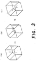
- Fig. 3 is a diagram for illustrating the principle of a resonator which excites three resonance successively, (a) is indicating resonance of a direction z is on a first stage of a filter, (b) is indicating resonance in a direction x on a second stage and (c) is indicating resonance in a direction yon a third stage,
- Fig. 4 is a diagram for illustrating how the coupling can be varied in the event of varying the size of the ridge portion to be chamfered, (a) is showing a graph indicating the result and (b) is showing how to take a size C of the ridge portion to be chamfered and a size L of whole surface including the above-mentioned chamfered portion,
- Fig. 5 is a perspective diagram for showing a dielectric filter of the example 1 utilizing a triple mode dielectric resonator
- Fig. 6 is a diagram for showing an example of characteristics of the dielectric filter shown in Fig. 5, (a) is showing a relation between insertion loss and return loss with frequency and (b) is showing a wide band characteristics of transmission loss,
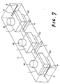
- Fig. 7 is a perspective diagram for showing a comparative example 1 of a dielectric filter with three stages utilizing conventional TE11 ⁇ mode,
- Fig. 8 is a perspective diagram for showing a comparative example 2 of a dielectric filter utilizing conventional HE11 ⁇ dual mode
- Fig. 9 is showing pass band characteristics of the dielectric filter of the comparative example 2 shown in Fig. 8,
- Fig. 10 is a perspective diagram for showing a dielectric filter of an example 2 utilizing two triple mode dielectric resonators
- Fig. 11 is a perspective diagram for showing a dielectric filter of an example 3 providing a dielectric filter utilizing two triple mode dielectric resonators with a metallic partition between two dielectric blocks,
- Fig. 12 is a diagram for showing a frequency characteristic of the dielectric filter shown in Fig. 11,
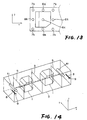
- Fig. 13 is a diagram showing a method of adjusting the dielectric filter by using a metal rod
- Fig. 14 is a perspective diagram for showing a dielectric filter with eight stages relative to the example 5 consisting of a combination of a triple mode dielectric resonator of the present invention and a metallic TEM mode resonator,
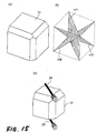
- Fig. 15 is a diagram for illustrating a triple mode dielectric resonator relative to a second preferred embodiment of the present invention
- (a) is a diagram for showing a basic composition of the triple mode dielectric resonator
- (b) is a diagram for showing planes existing each electric field of the triple mode resonance in the dielectric resonator
- (c) is a diagram for showing a method of exciting a single mode (in other word, exciting in a degenerated state) in the dielectric resonator
- Fig. 16 is a diagram for showing pass band characteristics and return loss in the event of exciting a single mode (in other word, exciting in a degenerated state) as shown in Fig. 5 (c),
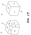
- Fig. 17 is a diagram for showing a dielectric resonator of an example 1, (a) is a perspective view of the dielectric resonator observed from a certain point of view and (b) is a perspective view of the dielectric resonator observed from another point of view,
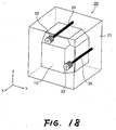
- Fig. 18 is a diagram for showing a composition of the dielectric filter mounting a dielectric resonator of the example 1 therein,
- Fig. 19 is showing pass band characteristics and return loss of a dielectric filter shown in Fig. 18,
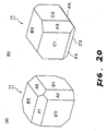
- Fig. 20 is a diagram for showing a dielectric resonator of the example 2, (a) is a perspective view of the dielectric resonator observed from a certain point of view and (b) is a perspective view of the dielectric resonator observed from another point of view.
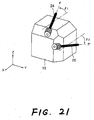
- Fig. 21 is a diagram for showing a relation between a dielectric resonator and a feeding probe of the example 3,
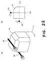
- Fig. 22 is a diagram for showing a relation between a dielectric resonator and a feeding probe of an example 4, (a) is a diagram for showing main portion of the dielectric filter of the example 4 and (b) is a diagram for showing an installing position of the feeding probe,
- Fig. 23 is a diagram for showing attenuation characteristics of the dielectric filter of the example 4.
- Fig. 24 is a diagram for illustrating an event of using plural dielectric resonators, (a) is a diagram for showing an example 5 using two dielectric resonators and (b) is a diagram for showing an example 6 applying four dielectric resonators to a duplexer.
- Fig. 1 is a perspective diagram for showing a triple mode dielectric resonator relative to a first preferred embodiment of the present invention.
- the triple mode dielectric resonator relative to the present preferred embodiment is composed of combination of three resonant modes in one dielectric block 1 by having a surface 2a formed by chamfering a ridge portion of a dielectric block 1 of a generally rectangular parallelopiped and a surface 2b formed by chamfering another ridge portion which is not parallel to the above-mentioned ridge portion.
- axes x, y, z is shown separately from the dielectric block 1 in Fig. 1, the axes x, y, z are in a relation to be orthogonal to each of two surfaces of the dielectric block 1 of a generally rectangular parallelopiped. And the relation is taken over in the following drawings.
- a tangent component (component y) of the electric field reflects in a 90-degrees direction on the surface 2a and propagates in the direction x. That is, component y in the propagation direction z reflects on the surface 2a and becomes component y in the propagation direction x. Electric wave generated in the direction x also repeats reflections at the interface surface similar to the direction z and excites resonance.
- the dielectric block 1 has the surface 2b which is formed by chamfering a ridge portion parallel to the axis z, resonance in the direction y is excited and three resonance are excited successively by one resonator.
- the direction z is on a first stage, as shown in Fig. 3 (a)
- the direction x is on a second stage, as shown in Fig. 3 (b)
- the direction y is on a third stage, as shown in Fig. 3 (c).
- the dielectric block is a cube, resonant frequency on the second stage is raised higher.
- the size of the dielectric block 1 can be shortened on the second stage, that is, in the direction x.
- the surface 2a with a chamfered ridge portion is a coupling of the first and the second stages and the surface 2b with a chamfered ridge portion is a combination of the second and the third coupling.
- Fig. 4 The result of checking for how the coupling varies in the event of changing the size of chamfering the above-mentioned ridge portion is shown in Fig. 4.
- a size C of the chamfered ridge portion of the dielectric block 1 of a generally rectangular parallelopiped and a size L of the whole surface including the chamfered portion variation of coefficients of coupling is checked for in four events of varying C/L.
- Fig. 4 (a) As an occupied rate of the size L of the whole by the size C of the chamfered ridge portion goes up, so does the coefficients of the coupling monotonously. Therefore, the coupling can be intensified, as the size of the chamfered ridge portion is taken larger in the dielectric block 1.
- Fig. 5 is a perspective diagram of a dielectric filter of an example 1 in which one of the above-mentioned triple mode dielectric resonator is used. That is, as shown in Fig. 5, the dielectric filter of the present example is composed of a triple mode dielectric resonator 50 disposed in a cut-off wave guide 3, in which three resonant modes of a dielectric block 1 of a generally rectangular parallelopiped are coupled by forming a surface 2a by chamfering a ridge portion and a surface 2b by chamfering a ridge portion on the dielectric block 1 and two rod-type antennas 8, 8 having a tip respectively opened by input- output terminals 9, 9 are provided as means for excitation.
- the dielectric filter of the present example is composed of a triple mode dielectric resonator 50 disposed in a cut-off wave guide 3, in which three resonant modes of a dielectric block 1 of a generally rectangular parallelopiped are coupled by forming a surface 2a by chamfering
- the antennas 8, 8 with an open tip are used as means for excitation of the dielectric resonator 50.
- the dielectric resonator 50 is supported by dielectrics with low dielectric constant, and the like in order not to contact with the cut-off waveguide 3, while the dielectrics with low dielectric constant is abbreviated in the present diagram.
- Characteristics example of the dielectric filter shown in Fig. 5 is shown in Figs. 6 (a) and (b).
- Fig. 6 (a) three poles of return loss appear and that indicates characteristics corresponding to the characteristics of a filter with three stages is obtained.
- Fig. 6 (b) it is apparent that two attenuation poles 62, 64 are generated on a side of higher frequency than center frequency.
- Fig. 7 is a perspective diagram for showing a comparative example 1 of a dielectric filter with three stages using a conventional TE11 ⁇ mode. That is, the dielectric filter of the comparative example 1 is composed of three dielectric blocks 1 putting a predetermined distance to each other disposes in a longitudinal cut-off waveguide 3 and rod-type antennas 8, 8 having a tip respectively opened by input- output terminals 9, 9 provided as means for excitation at both ends in a longitudinal direction of the cut-off waveguide 3. And screws 4, 4 having one end respectively contacting with the cut-off waveguide 3 are disposed between each of three dielectric blocks 1 in order to adjust the coupling between the dielectrics.
- 40 indicates mounts for supporting each resonator (dielectric block 1) and resonant frequency of each resonator (dielectric block 1) is adjusted by each metal rod 42.
- the dielectric filter according to the example 1 shown in Fig. 5 is larger to some extent than the one according to the comparative example 1 shown in the above-mentioned Fig. 7, though a certain amount of distance corresponding to the coupling is required between a dielectric block 1 and another dielectric block 1, as shown in Fig. 7.
- a certain amount of distance corresponding to the coupling is required between a dielectric block 1 and another dielectric block 1, as shown in Fig. 7.
- the above-mentioned distance is not required and the volume of whole filter is possibly one third of the comparative example 1.
- Fig. 8 is a perspective diagram for showing a comparative example 2 of a dielectric filter using a conventional HE11 ⁇ dual mode. That is, the dielectric filter is composed of a cylindrical dielectric block 1 supported by dielectrics with low dielectric constant, and the like (not shown) in order not to contact with a cut-off waveguide 3 disposed in the cylindrical cut-off waveguide 3 and rod-type antennas 8, 8 having a tip respectively opened by input-output terminals 9, 9 provided at both ends of the cut-off waveguide 3 varying the angles to each other.
- Two resonance in the dual mode dielectric resonator are adjusted with the coupling by a metal rod 13.
- Pass band characteristics of the dielectric filter of the comparative example 2 shown in Fig. 8 are shown in Fig. 9.
- Fig. 9 shows the same band as the Fig. 6.
- Fig. 10 is a perspective diagram of a dielectric filter of an example 2 utilizing two of the above-mentioned triple mode dielectric resonators therein. That is, the dielectric filter of the example 2 is composed of two of the triple mode dielectric resonators shown in Fig. 1 putting a predetermined distance to each other disposed in a longitudinal cut-off waveguide 3 and rod-type antennas 8, 8 having both end surfaces opened by input-output terminals 9, 9 provided in a direction of axis x from the above-mentioned both end surfaces in longitudinal direction of the cut-off waveguide 3 respectively.
- a screw 4 contacting with upper surface of the cut-off waveguide 3 by one end is disposed between the two triple mode dielectric resonators in order to adjust the coupling between the dielectrics.
- mounts for supporting each resonator are abbreviated in the present diagram as well.
- two of the triple mode dielectric resonators are provided, which makes totally six stages of filter.
- a metal rod (screw) 4 is inserted between the resonators in order to couple the two dielectric resonators strongly by resonance in the direction y.
- Fig. 11 is a perspective diagram of a dielectric filter of an example 3 which is a dielectric filter utilizing the above-mentioned triple mode dielectric resonators providing a metallic partition 5 between two dielectric blocks 1 therein. That is, in the same manner as the above-mentioned example 2, the dielectric filter of the example 3 is composed of two of the triple mode dielectric resonators shown in Fig. 1 disposed in a longitudinal cut-off waveguide 3 and rod-type antennas 8, 8 having both end surfaces opened by input-output terminals 9, 9 provided in a direction of axis x from the above-mentioned both end surfaces in longitudinal direction of the cut-off waveguide respectively.
- a metallic partition 5 is provided instead of a screw 4 of the example 2 between the two dielectric resonators.
- a surface 2b having the above-mentioned another ridge portion chamfered on one side of the dielectric block 1 is formed in a different position from the surface of the example 2 shown in Fig. 10.
- mounts for supporting each resonator (dielectric block 1) are abbreviated in the present diagram as well.
- a frequency characteristic of the dielectric filter is shown in Fig. 12.
- a coupling between resonators by resonance in direction x and direction z can be weakened by the metallic partition 5 and the coupling between the resonators can be mainly obtained by the resonance in direction y.
- attenuation poles 122, 124 can be provided respectively on both of low frequency side and high frequency side of the pass band by using a shape of resonator of the example 3 shown in Fig. 11, means for excitation and metallic partition 5.
- Fig. 13 is a diagram for showing a method of adjusting the above-mentioned dielectric filter by a metal rod.
- a screw is used as a metal rod and the adjustment is conducted by putting in and out of the screw.
- the metal rod acts on a magnetic field leaking from dielectrics.
- the metal rod in the position of 6a in Fig. 13 has interlinkage with magnetic flux of the resonance in the event of resonance in direction x, the magnetic field is intensified and resonant frequency becomes lower.
- the phenomenon is equal to a growth of equivalent inductance in a parallel resonant circuit.
- 6b lowers the resonant frequency of y direction.
- Fig. 14 is a perspective diagram for showing a dielectric filter with eight stages composed of combination of a triple mode dielectric resonator of the present invention and a TEM mode resonator made of metal relative to an example 5. That is, the dielectric filter of the example 5 is composed of two of the triple mode dielectric resonators shown in Fig. 1 putting a predetermined distance to each other disposes in a cut-off waveguide 3 and a TEM mode resonator 41 made of metal disposed on both sides of the resonators. Incidentally, rod-type antennas 8, 8 opened by input-output terminals 9, 9 are provided in a direction of axis y at both end portions of the cut-off waveguide 3.
- the filter can be composed of stages by multiples of three, however, a filter composed of stages of arbitrary numbers can be composed by combining the triple mode dielectric resonator of the present invention and, for example, a resonator of single TE01 ⁇ mode of dielectrics according to a prior art, and the like. And as shown in Fig. 14, undesired resonance can be suppressed by combing the TEM mode resonator 41 instead.
- Fig. 15 (a) is a diagram for showing a fundamental composition of a triple mode dielectric resonator relative to the second preferred embodiment of the present invention
- Fig. 15 (b) is a diagram for showing planes existing each electric field of the triple mode resonance in the dielectric resonator shown in Fig. 15 (a).
- the dielectric resonator 10 of the present preferred embodiment consists of dielectric blocks generally cube-type with three ridge portions chamfered and characterized in generating TE01 ⁇ mode in electro-magnetically independent three surfaces m1, m2, m3 of the dielectric block, as shown in Fig. 15 (b).
- the electro-magnetically independent three resonant modes are generated on each surface of m1, m2, m3 and an angle of 60.0 degrees is offered between each surface of m1, m2, m3, in Fig. 15 (b).
- Fig. 15 (c) is a diagram for showing a method of exciting a single mode (in other word, exciting in the degenerated state) in the dielectric resonator shown in Fig. 15 (a).
- feeding probes 24 and 25, for example are disposed in the same direction on an opposing surface to the dielectric block to excite a single mode.
- Fig. 16 is a diagram for showing pass band characteristics in the event of exciting only a single mode (in other word, exciting in the degenerated state), as Fig. 15 (c).
- the pass band characteristics in the above-mentioned event is indicated by a solid line and return loss is indicated by a dotted line respectively.
- Dielectric resonators of the present example are shown in Figs. 17 (a) and (b).
- Figs. 17 (a) and (b) are diagrams for showing the same dielectric resonator 10 observed from different viewpoints respectively.
- a dielectric block consisting of dielectric materials of BaO-TiO2 system providing relative dielectric constant ⁇ ⁇ of 37 is used in the dielectric resonator 10 of the present example.
- ridge portions sharing one point of a dielectric block consisting of a cube with a side of 22mm are chamfered in order to offer an angle of 45 degrees to the surface of the dielectric block and each surface of A1, A2, A3 and each surface of A1, A2, A3 is formed in plane having a width of approximately 7mm respectively; as shown in Fig. 17 (a).
- a surface B1 adjacent to the surfaces A2, A3, a surface B2 adjacent to the surfaces A1, A3 and a surface B3 adjacent to the surfaces A1, A2 are respectively formed.
- the surfaces B1, B2, B3 are squares with a side of 17mm (17mm x 17mm). Therefore, in the present example, area ratios of the surfaces A1, A2, A3 with respect to the surfaces B1, B2, B3 respectively are approximately 45%.
- each of surfaces C (surface C2 opposing to surface B1, surface C1 opposing to surface B3, surface C3 opposing to surface B2) opposing to the surfaces B is shaped in a square with a side of 22mm (22mm x 22mm) having one corner clipped by an isosceles triangle with two sides of 5mm and one side of 7mm.
- the portion in which the surfaces A (A1, A2, A3) transposition is formed in a triangular cone there is no problem in the characteristic to chamfer the triangular cone portion to be plane.
- Fig. 18 is a diagram for illustrating a dielectric filter 20 mounting the dielectric resonator 10 of the example 1 in a cut-off waveguide 21 of a generally rectangular parallelopiped.
- axes x, y, z are shown separately from the dielectric resonator 10 in Fig. 18, each of axes x, y, z is in relation orthogonal to each of two surfaces of the dielectric block of the original cube of the dielectric resonator 10. The same thing takes place in the following drawings.
- the dielectric filter 20 is formed by disposing the dielectric resonator 10 shown in Figs.
- the dielectric filter 20 provides feeding probes 22, 23 disposed at two positions therein.
- a rod-type material is used as feeding probes 24, 25.
- Direction p (not shown) of the two feeding probes 24 and 25 is parallel to the axis x with respect to axes x, y, z of the dielectric resonator 10, therefore, an angle p' (not shown) offered by the feeding probes 24 and 25 is 0 degree.
- Fig. 19 pass band characteristics of the dielectric filter 20 is indicated by a solid line and return loss is indicated by a dotted line, respectively.
- dielectric filter 20 of the present example has a pass band between 1.916 [GHz] and 1.934 [GHz], both inclusive. Further, in Fig. 19, poles of return loss 51, 52, 53 indicate that a three-stage band pass filter is formed by the dielectric filter 20 of the present example.
- FIGs. 20 (a) and (b) are diagrams of the same dielectric resonator 11 observed from different points of view respectively.
- a dielectric block consists of dielectric material of BaO-TiO2 system providing relative dielectric constant ⁇ ⁇ of 37 is used in the dielectric resonator 10 of the present example in the same manner as the example 1.
- the dielectric resonator 11 of the present example has three surfaces A (A1, A2, A3) formed by chamfering three ridge portions sharing one point of a dielectric block, as shown in Fig. 20 (a) and three surfaces A'4, A'5, A'6 (hereafter called surfaces A') further formed by chamfering three ridge portions sharing another point on diagonal line of the above-mentioned point.
- an angle offered by the three surfaces A or by three surfaces A' with other adjacent three surfaces B'1, B'2, B'3 [refer to Fig. 20 (a)] (hereafter called as surfaces B') or with other adjacent three surfaces C'1, C'2, C'3 [refer to Fig. 20 (b)] (hereafter called as surfaces 'C) respectively is 45 degrees.
- a dielectric resonator 11 of the present example For manufacturing a dielectric resonator 11 of the present example, three ridge portions sharing one point of a dielectric block consisting of a cube with a side of 22mm (22mm x 22mm x 22mm) is chamfered so that the surface of the dielectric block and surfaces A1, A2, A3 offers 45 degrees respectively and each of the surfaces A1, A2, A3 is formed in plane with a width of 7mm, as shown in Fig. 20 (a).
- three ridge portion sharing another point on a diagonal line of the above-mentioned point is chamfered so that the surface of the dielectric block and surfaces A4', A5', A6' offers 45 degrees respectively and each of the surfaces A4', A5', A6' is formed in plane with a width of 7mm, as shown in Fig. 20 (b).
- a surface B'1 adjacent to the surfaces A2, A3, a surface B'2 adjacent to the surfaces A1, A3 and a surface B'3 adjacent to the surfaces A1, A2 are respectively formed and a surface C'1 opposing to the surface B'3, a surface C'2 opposing to the surface B'1 and a surface C'3 opposing to the surface B'2 are formed respectively.
- the surfaces B'1, B'2, B'3 are squares with a side of 17mm (17mm x 17mm) chamfered by one corner thereof.
- the area ratio of the surfaces A with respect to the surfaces B' is approximately 48% in the present example, which gets slightly larger than the above-mentioned example 1.
- the areas and forms of the surfaces C' opposing to the surfaces B' are similar to the surfaces B'.
- a similar dielectric filter can be formed by mounting the dielectric resonator 11 of the present example 7 in a cut-off waveguide of a generally rectangular parallelopiped, in the same manner as the example 6.
- a main portion of a dielectric filter of the present example is shown in Fig. 21.
- the dielectric filter of the present example is a dielectric filter mounting the dielectric resonator 10 similar to the one of example 6 shown in Figs. 17 (a) and (b) in a cut-off waveguide if a generally rectangular parallelopiped, but only the dielectric resonator 10 and feeding probes 24 and 25 are shown in Fig. 21.
- the direction p can be varied within the range between -45 degrees and +45 degrees, both inclusive
- the direction p' can be varied within the range between -45 degrees and +45 degrees, both inclusive.
- a main portion of a dielectric filter of the present example is shown in Fig. 22 (a).
- the dielectric filter of the present example is a dielectric filter mounting the dielectric resonator 10 similar to the one of example 6 shown in Figs. 17 (a) and (b) in a cut-off waveguide of a generally rectangular parallelopiped, but only the dielectric resonator 10 and feeding probes 24 and 25 are shown in Fig. 22 (a).
- the feeding probes 24 and 25 are provided on the surfaces B [the surfaces B2 in Fig. 17 (a)] and the surfaces C [the surfaces C2 in Fig. 17 (b)] of the dielectric resonator 10. Positions for disposing the feeding probes 24 and 25 are shown in Fig. 22 (b).
- Fig. 22 (b) is a diagram of the dielectric resonator 10 and the feeding probes 24 and 25 observed from a direction of axis x.
- Directions p (not shown) and p' (not shown) of the feeding probes 24 and 25 are parallel to the axis x, as shown in Fig. 22 (b) and the feeding probes 24 can be displaced in parallel with the axis y and the feeding probes 25 can be displaced in parallel with the direction of axis z, as shown in Fig. 22 (b).
- Fig. 22 (b) movement of the feeding probes 24 and 25 to approach to each other is indicated as a (refer to the diagram).
- Fig. 23 the attenuation characteristics of the dielectric filter of the present example are shown.
- an attenuation pole 90 is generated at frequency of approximately 1.873 [GHz].
- the attenuation pole is obtained on a side of lower frequency than a center frequency, that is, on a lower side band.
- the present example is an example using four dielectric resonators 10, as shown in Fig. 24 (b).
- the present example is an example for applying a dielectric filter 150 combined for transmitting and for receiving using two dielectric resonators 10 and a duplexer 200 is composed.
- the angle offered by the three surfaces A formed by chamfering three ridge portions sharing one point of the dielectric block and another three surfaces B or B' adjacent thereto is set at 45 degrees, the similar effect can be obtained by an angle in the range between 40 degrees and 50 degrees, both inclusive.
- the angle offered by the three surfaces A' formed by chamfering three ridge portions sharing an apex of the dielectric block and another three surfaces C' adjacent thereto is set at 45 degrees, the similar effect can be obtained by an angle within the range between 40 degrees and 50 degrees, both inclusive.
- the area ratio of the surfaces A with respect to the surfaces B is set 45%, the similar effect can be obtained by an area ratio within the range between 1% and 200 %, both inclusive.
- a triple mode dielectric resonator which is capable of acting as three resonators with one dielectric block, as described above.
- the triple mode dielectric resonator it is possible to achieve size reduction of dielectric filters.
- weight and the number of required resonator can be reduced and the cost can be saved consequently.
- a dielectric resonator relative to a second preferred embodiment of the present invention has a dielectric block formed by chamfering three ridge portion of a generally rectangular parallelopiped and effects a degenerate coupling of the triple mode (TE01 ⁇ mode) of the equal resonant frequency generated on three surfaces which are electro-magnetically independent of the above-mentioned dielectric block, it is possible for a very small dielectric resonator with a simple composition to be realized easily, while resonance of triple mode is available.
- a small sized dielectric filter with a simple composition can be provided.
Landscapes
- Control Of Motors That Do Not Use Commutators (AREA)
Abstract
Description
- The present invention relates to a dielectric filter used in radio communications, and the like at high frequency band as microwave band, quasi-microwave band, and the like and a dielectric resonator used in the dielectric filter, and more particularly to a triple mode dielectric resonator in which three resonant modes are available in one dielectric block and a dielectric filter using the dielectric resonator therein.
- Conventionally, a dielectric filter which providing a cut-off waveguide with cylindrical or rectangular parallelopiped dielectrics disposing successively therein and utilizing resonance of a cylindrical TE01δ mode or a rectangular TE11δ mode of dielectrics is utilized widely in filters requiring low loss and size reduction, because the dielectric filter has high unloaded Q and can be reduced in size easier than waveguide type filter (a first conventional example). A resonance of the mode is generated by an electric field repeating reflections at an interface surface of the dielectric resonator and the air. The resonant frequency of dielectric resonator is inversely proportional to the length of the resonator and square root of dielectric constant, so that the larger the dielectric constant is, the smaller the resonator is. And a magnetic field generated by the resonance excites a resonator on the next stage and the excitation corresponds to the coupling between stages of the dielectric filter. As a magnitude of the coupling is mainly determined by the distance between resonators, the farther the distance is, the weaker the coupling is. As adjusting means for the above-mentioned dielectric filter, a method of adjusting the resonant frequency by a screw in a direction orthogonal to the reflecting surface of the magnetic field or a method of adjusting the coupling between the resonators by a screw, and the like are adoptable.
- And there is also a dielectric filter utilizing a dual mode dielectric resonator in order to achieve size reduction (a second conventional example). The above-mentioned dielectric resonator provides two resonance by one resonator, in which a cylindrical dielectric resonator is disposed in the center of a cylindrical waveguide by justifying the axes of the cylinders, for example, and two resonance (HE11δ) generated in two directions orthogonal to the axes of the cylinders are coupled by disturbing the electromagnetic field of the resonance from the waveguide side using means as screws, and the like.
- As the description about a first conventional example above, the resonant frequency of the resonator by a cylindrical TE01δ mode or a rectangular TE11δ mode of dielectrics depends on dielectric constant and the size of dielectrics and a resonator can be smaller when the dielectric constant gets larger, accordingly the simplest method of reducing size of the filter utilizing the dielectric resonator is to raise the dielectric constant of dielectrics.
- However, as dielectrics with low dielectric loss used in microwave region generally has a characteristic that dielectric loss thereof increases as dielectric constant becomes higher, size reduction of the filter maintaining insertion loss low has a certain limitation. Further, as dielectrics with low loss as mentioned above is expensive, accordingly the filter becomes expensive when the filter provides more stages, that is, provides more dielectrics used therein.
- And a filter relative to a second conventional example utilizing HE11δ dual mode dielectric resonator for size reduction has a problem that lots of undesired modes excited in the vicinity of pass band result in spurious characteristic deteriorated easily, because HE11δ is not the dominant mode.
- On the other hand, for example, in the event that a dielectric filter used in microwave communications, and the like is composed, it is conventionally hard to reduce size and weight of a dielectric filter, because many resonators and each spaces between the resonators occupies large amount of volume and weight according to the requirement of one resonator for one resonance and space for coupling between each resonator. Therefore, there still is a problem that the dielectric filter is unavoidably composed complicated and large, even though it is a band pass filter using dielectric resonators of relatively small size.
- Consequently, composing a dielectric filter using dielectric resonators capable of multiple mode resonance is proposed to realize a band pass filter with a very small and simple composition exploiting advantages in using dielectric resonators fully. For example, size reduction of a band pass filter having a double-tuned band characteristic by varying the resonant frequency of the two resonance modes to each other is proposed in unexamined Japanese Patent Publication No. Hei 7-58516, in which degenerate coupling of two resonance modes with respect to TE101 and TE01δ modes is disclosed (a third conventional example). And a multiple mode dielectric resonator capable of generating TM01δ mode and TE01δ mode which are generated on a surface parallel to each surface (x-y surface, y-z surface, x-z surface) in a rectangular coordinate system in a generally rectangular parallelopiped shaped dielectric block is proposed in unexamined Japanese Patent Publication No. Hei 11-145704 (a fourth conventional example).
- However, it is still unavoidable that a dielectric resonator occupies a large amount of volume in a band pass filter requiring a resonator of multiple stages, even though the degenerate coupling of two resonance modes relative to the above-mentioned third conventional example as described in unexamined Japanese Patent Publication No. Hei 7-58516 is utilized. And even a triple mode dielectric resonator relative to the fourth example as described in unexamined Japanese Patent Publication No. Hei 11-145704 has a problem that the manufacturing process becomes complicated, because utilization of hybrid coupling of TM01δ mode and TE01δ mode which are orthogonal spatially requires the thickness of dielectric resonator to be adjusted to resonant frequency.
- It is therefore a first object of the present invention to realize a dielectric filter capable of reducing the number of dielectric resonators to a large extent, aiming at size reduction and cost reduction and providing favorable out-of-band characteristic by incorporating the mode which has been undesired into the band and activating the mode as a portion of resonance necessary for filter characteristic exploiting advantages that unloaded Q of the dielectric filter by a cylindrical TE01δ mode or a rectangular TE11δ mode relative to a first and a second conventional examples is high.
- And a second object of the present invention is to solve the problem of the above-mentioned third and fourth conventional examples and to provide a very small dielectric resonator with simple composition in spite of enabling a triple mode resonance and a dielectric filter using the above-mentioned dielectric resonator.
- The present invention aims at size reduction of dielectric filter by using three resonant modes in one dielectric block in order to achieve a first object of the above-mentioned present invention. That is, in a block of a generally rectangular parallelopiped consisting of dielectric material, three, resonant modes in a single dielectric block can be coupled by chamfering a ridge portion of the dielectric block and another ridge portion unparallel thereto.
- That is, the dielectric resonator claimed in
claim 1 is characterized in combining three resonant modes of the above-mentioned dielectric block by removing one ridge portion and another ridge portion unparallel thereto in a block of a generally rectangular parallelopiped. - It is apparent from physical symmetry characteristics that a rectangular TE11δ mode can exist in each of three orthogonal axial direction in a block of a generally rectangular parallelopiped. In a conventional dielectric
filter using TE11 6 mode or HE11δ mode, the filter is composed using only one or two resonance out of the above-mentioned resonance of three axial direction, while the rest of the resonance exerts a harmful effect as undesired resonance. In the present invention, the rest of the resonance is utilized positively so that one resonator acts as three resonators. - And a dielectric filter claimed in claim 2 is characterized in disposing at least one dielectric resonator claimed in
claim 1 in a cut-off waveguide. - Because a small dielectric filter with low insertion loss can be manufactured by composing a filter in which one or more of the above-mentioned dielectric resonators are disposed in the cut-off waveguide.
- Further, a dielectric filter claimed in
claim 3 is characterized in disposing two or more of the above-mentioned dielectric resonators in the above-mentioned cut-off waveguide and providing means for partition consisting of electric conductive material between the above-mentioned dielectric resonators. - Because, in the event of using plural of resonators, it becomes possible to adjust the coupling of each mode between resonators properly, to take required coupling for the pass band characteristics and to form an attenuation pole out of the pass band by providing conductive partitions between each of the resonators.
- And a dielectric filter claimed in
claim 4 is characterized in disposing a metal rod contacting with the above-mentioned waveguide by one end parallel to a side surface of the above-mentioned dielectric resonator in a position away from the above-mentioned side surface by a predetermined distance, in which resonant frequency of each resonance and the coupling between each of the resonance are adjustable depending on the length of the above-mentioned metal rod. - Because, a filter using a triple mode dielectric resonator according to the present invention is capable of adjusting resonant frequency and the amount of coupling by putting a metal rod as a screw from the cut-off waveguide parallel to the side surface of the dielectric resonator in the position away from the side surface of the dielectric resonator by a predetermined distance and occupying adjustable range of the filter widely by combining above-mentioned operation with conventional means for adjusting.
- Incidentally, a dielectric filter claimed in
claim 5 is characterized in further installing a resonator other than the dielectric resonator claimed inclaim 1 in the above-mentioned waveguide as well. - Because, a small filter with an arbitrary number of stage can be composed by combining the triple mode dielectric resonator according to the present invention and resonators of dielectrics TE01δ mode or TEM mode by metallic conductor, and the like. Besides, out-of-band characteristics all over the filter can be improved by using a resonator with less undesired resonance or with undesired resonance located away from the necessary band as the above-mentioned combined resonator.
- On the other hand, in the present invention, a dielectric resonator is composed of a dielectric block of a generally rectangular parallelopiped with three ridge portions chamfered thereof and TE01 δ mode is generated on the electro-magnetically individual three surfaces of the above-mentioned dielectric block as claimed in
claim 6 in order to achieve the above-mentioned second object of the present invention. - Incidentally, it is preferable for the above-mentioned dielectric block to be mounted in a cut-off waveguide of a generally rectangular parallelopiped as claimed in claim 7.
- And a dielectric resonator claimed in
claim 8 is characterized in having three surfaces of A1, A2, A3 (hereafter called surfaces A) formed by chamfering three ridge portions sharing an apex of the above-mentioned dielectric block and three surfaces of B1, B2, B3 (hereafter called surfaces B) adjacent to each of the surfaces A respectively, in which an angle between 40 degrees and 50 degrees, both inclusive, is offered by the surfaces A and B and an area ratio of the above-mentioned surfaces A with respect to the surfaces B stands between 1% and 200%, both inclusive. - Further, a dielectric resonator claimed in
claim 9 is characterized in having three surfaces A formed by chamfering three ridge portions sharing an apex of the above-mentioned dielectric block, another three surfaces of A'4, A'5, A'6 (hereafter called surfaces A') formed by chamfering three ridge portions sharing another apex on a diagonal line of the above-mentioned point, another three surfaces of B'1, B'2, B'3 (hereafter called surfaces B') adjacent to each of surfaces A and surfaces A' respectively and still another three surfaces of C'1 C'2 C'3 (hereafter called surfaces C') adjacent to each of surfaces A and surfaces A' respectively, in which an angle between 40 degrees and 50 degrees, both inclusive, is offered by the surfaces A and B' or by the surfaces A' and C' and an area ratio of the above-mentioned surfaces A with respect to the above-mentioned surfaces B' or an area ratio of the above-mentioned surfaces A' with respect to the above-mentioned surfaces C' stand between 1% and 200%, both inclusive, respectively. - On the other hand, a dielectric filter claimed in
claim 10 is a dielectric filter using a dielectric resonator, in which an angle between 40 degrees and 50 degrees, both inclusive, is offered by the above-mentioned three surfaces A or A' and other three surfaces B or B' adjacent thereto respectively and the surfaces A or A' and surfaces B or B' adjacent thereto respectively have three opposing surfaces of C1, C2, C3 (hereafter called surfaces C) or the surfaces C' and characterized in providing a feeding probe near the surfaces B and B', the surfaces B' and B', the surfaces C and C', or the surfaces C' and C'. - And a dielectric filter claimed in
claim 11 is a dielectric filter using a dielectric resonator having the above-mentioned three surfaces A formed by chamfering three ridge portion sharing an apex of the above-mentioned dielectric block, another three surfaces B adjacent to the above-mentioned three surfaces A forming an angle of 40 degrees through 50 degrees and three surfaces C opposing to the above-mentioned three surfaces B respectively, in which a feeding probe is provided on the surfaces B and surfaces C. - Incidentally, as a dielectric filter claimed in claim 12, an angle offered by direction p and p' of the feeding probe with respect to the x, y, z axes of the above-mentioned dielectric resonator are variable within the range of -45 degrees through +45 degrees while in use.
- And as a dielectric filter claimed in
claim 13, frequency and attenuation generating the attenuation pole at a lower side band can be varied by varying a position for providing a feeding probe on the above-mentioned surfaces B and a position for providing a feeding probe on the above-mentioned surfaces C respectively. - Here, either of rod-type as claimed in claim 14 or loop-type as claimed in
claim 15 is acceptable as the above-mentioned feeding probe. - Further, as claimed in claim 16, a dielectric filter capable of being applied to various kinds of application can be composed by mounting two or more of the above-mentioned dielectric resonators in the above-mentioned cut-off waveguide of a generally rectangular parallelopiped therein.
- Fig. 1 is a perspective diagram for showing a triple mode dielectric resonator relative to a first preferred embodiment of the present invention,
- Fig. 2 is a diagram for illustrating resonance of rectangular TE11δ mode, (a) is indicating a direction to which an electric field acts and (b) is indicating a direction to which a magnetic field acts respectively,
- Fig. 3 is a diagram for illustrating the principle of a resonator which excites three resonance successively, (a) is indicating resonance of a direction z is on a first stage of a filter, (b) is indicating resonance in a direction x on a second stage and (c) is indicating resonance in a direction yon a third stage,
- Fig. 4 is a diagram for illustrating how the coupling can be varied in the event of varying the size of the ridge portion to be chamfered, (a) is showing a graph indicating the result and (b) is showing how to take a size C of the ridge portion to be chamfered and a size L of whole surface including the above-mentioned chamfered portion,
- Fig. 5 is a perspective diagram for showing a dielectric filter of the example 1 utilizing a triple mode dielectric resonator,
- Fig. 6 is a diagram for showing an example of characteristics of the dielectric filter shown in Fig. 5, (a) is showing a relation between insertion loss and return loss with frequency and (b) is showing a wide band characteristics of transmission loss,
- Fig. 7 is a perspective diagram for showing a comparative example 1 of a dielectric filter with three stages utilizing conventional TE11δ mode,
- Fig. 8 is a perspective diagram for showing a comparative example 2 of a dielectric filter utilizing conventional HE11δ dual mode,
- Fig. 9 is showing pass band characteristics of the dielectric filter of the comparative example 2 shown in Fig. 8,
- Fig. 10 is a perspective diagram for showing a dielectric filter of an example 2 utilizing two triple mode dielectric resonators,
- Fig. 11 is a perspective diagram for showing a dielectric filter of an example 3 providing a dielectric filter utilizing two triple mode dielectric resonators with a metallic partition between two dielectric blocks,
- Fig. 12 is a diagram for showing a frequency characteristic of the dielectric filter shown in Fig. 11,
- Fig. 13 is a diagram showing a method of adjusting the dielectric filter by using a metal rod,
- Fig. 14 is a perspective diagram for showing a dielectric filter with eight stages relative to the example 5 consisting of a combination of a triple mode dielectric resonator of the present invention and a metallic TEM mode resonator,
- Fig. 15 is a diagram for illustrating a triple mode dielectric resonator relative to a second preferred embodiment of the present invention, (a) is a diagram for showing a basic composition of the triple mode dielectric resonator, (b) is a diagram for showing planes existing each electric field of the triple mode resonance in the dielectric resonator and (c) is a diagram for showing a method of exciting a single mode (in other word, exciting in a degenerated state) in the dielectric resonator,
- Fig. 16 is a diagram for showing pass band characteristics and return loss in the event of exciting a single mode (in other word, exciting in a degenerated state) as shown in Fig. 5 (c),
- Fig. 17 is a diagram for showing a dielectric resonator of an example 1, (a) is a perspective view of the dielectric resonator observed from a certain point of view and (b) is a perspective view of the dielectric resonator observed from another point of view,
- Fig. 18 is a diagram for showing a composition of the dielectric filter mounting a dielectric resonator of the example 1 therein,
- Fig. 19 is showing pass band characteristics and return loss of a dielectric filter shown in Fig. 18,
- Fig. 20 is a diagram for showing a dielectric resonator of the example 2, (a) is a perspective view of the dielectric resonator observed from a certain point of view and (b) is a perspective view of the dielectric resonator observed from another point of view.
- Fig. 21 is a diagram for showing a relation between a dielectric resonator and a feeding probe of the example 3,
- Fig. 22 is a diagram for showing a relation between a dielectric resonator and a feeding probe of an example 4, (a) is a diagram for showing main portion of the dielectric filter of the example 4 and (b) is a diagram for showing an installing position of the feeding probe,
- Fig. 23 is a diagram for showing attenuation characteristics of the dielectric filter of the example 4 and
- Fig. 24 is a diagram for illustrating an event of using plural dielectric resonators, (a) is a diagram for showing an example 5 using two dielectric resonators and (b) is a diagram for showing an example 6 applying four dielectric resonators to a duplexer.
- Referring to the drawings, explanation will be made for describing the present invention in detail, as follows.
- At first, a first preferred embodiment of the present invention is described. Fig. 1 is a perspective diagram for showing a triple mode dielectric resonator relative to a first preferred embodiment of the present invention. The triple mode dielectric resonator relative to the present preferred embodiment is composed of combination of three resonant modes in one
dielectric block 1 by having asurface 2a formed by chamfering a ridge portion of adielectric block 1 of a generally rectangular parallelopiped and asurface 2b formed by chamfering another ridge portion which is not parallel to the above-mentioned ridge portion. Incidentally, though axes x, y, z is shown separately from thedielectric block 1 in Fig. 1, the axes x, y, z are in a relation to be orthogonal to each of two surfaces of thedielectric block 1 of a generally rectangular parallelopiped. And the relation is taken over in the following drawings. - That is, now, in the orthogonal x-y-z coordinate system, the electric field is excited initially so that a direction z corresponds to a propagation direction of TE wave. Then an electric field repeats reflections in the direction z by 180-degrees reflection of the electric field at an interface surface of the dielectrics and the air and excites resonance of rectangular TE11δ mode at a certain frequency shown in Figs. 2 (a) and (b). However, as shown in Fig. 1, when the
dielectric block 1 has thesurface 2a which is formed by chamfering a ridge portion parallel to the axis y, a tangent component (component y) of the electric field reflects in a 90-degrees direction on thesurface 2a and propagates in the direction x. That is, component y in the propagation direction z reflects on thesurface 2a and becomes component y in the propagation direction x. Electric wave generated in the direction x also repeats reflections at the interface surface similar to the direction z and excites resonance. According to the similar principle, when thedielectric block 1 has thesurface 2b which is formed by chamfering a ridge portion parallel to the axis z, resonance in the direction y is excited and three resonance are excited successively by one resonator. What described above is the principle of the combination. Though the actual electric field in a resonator are degenerated so that components in three directions can exist concurrently, it is understandable that the direction z is on a first stage, as shown in Fig. 3 (a), the direction x is on a second stage, as shown in Fig. 3 (b), the direction y is on a third stage, as shown in Fig. 3 (c). When the dielectric block is a cube, resonant frequency on the second stage is raised higher. For adjusting three resonance frequencies, the size of thedielectric block 1 can be shortened on the second stage, that is, in the direction x. And with regard to the coupling, it can be understood that thesurface 2a with a chamfered ridge portion is a coupling of the first and the second stages and thesurface 2b with a chamfered ridge portion is a combination of the second and the third coupling. - The result of checking for how the coupling varies in the event of changing the size of chamfering the above-mentioned ridge portion is shown in Fig. 4. Here, by taking a size C of the chamfered ridge portion of the
dielectric block 1 of a generally rectangular parallelopiped and a size L of the whole surface including the chamfered portion, variation of coefficients of coupling is checked for in four events of varying C/L. As shown in Fig. 4 (a), as an occupied rate of the size L of the whole by the size C of the chamfered ridge portion goes up, so does the coefficients of the coupling monotonously. Therefore, the coupling can be intensified, as the size of the chamfered ridge portion is taken larger in thedielectric block 1. - Fig. 5 is a perspective diagram of a dielectric filter of an example 1 in which one of the above-mentioned triple mode dielectric resonator is used. That is, as shown in Fig. 5, the dielectric filter of the present example is composed of a triple
mode dielectric resonator 50 disposed in a cut-offwave guide 3, in which three resonant modes of adielectric block 1 of a generally rectangular parallelopiped are coupled by forming asurface 2a by chamfering a ridge portion and asurface 2b by chamfering a ridge portion on thedielectric block 1 and two rod-type antennas output terminals antennas dielectric resonator 50. Actually, thedielectric resonator 50 is supported by dielectrics with low dielectric constant, and the like in order not to contact with the cut-offwaveguide 3, while the dielectrics with low dielectric constant is abbreviated in the present diagram. Characteristics example of the dielectric filter shown in Fig. 5 is shown in Figs. 6 (a) and (b). As shown in Fig. 6 (a), three poles of return loss appear and that indicates characteristics corresponding to the characteristics of a filter with three stages is obtained. And as shown in Fig. 6 (b), it is apparent that twoattenuation poles - Fig. 7 is a perspective diagram for showing a comparative example 1 of a dielectric filter with three stages using a conventional TE11δ mode. That is, the dielectric filter of the comparative example 1 is composed of three
dielectric blocks 1 putting a predetermined distance to each other disposes in a longitudinal cut-offwaveguide 3 and rod-type antennas output terminals waveguide 3. And screws 4, 4 having one end respectively contacting with the cut-offwaveguide 3 are disposed between each of threedielectric blocks 1 in order to adjust the coupling between the dielectrics. Incidentally, 40 indicates mounts for supporting each resonator (dielectric block 1) and resonant frequency of each resonator (dielectric block 1) is adjusted by eachmetal rod 42. - With regard to volume of the
dielectric block 1, the dielectric filter according to the example 1 shown in Fig. 5 is larger to some extent than the one according to the comparative example 1 shown in the above-mentioned Fig. 7, though a certain amount of distance corresponding to the coupling is required between adielectric block 1 and anotherdielectric block 1, as shown in Fig. 7. As characteristics corresponding to a filter with triple stages can be obtained by onedielectric block 1 in the dielectric filter according to the example 1 shown in Fig. 5, the above-mentioned distance is not required and the volume of whole filter is possibly one third of the comparative example 1. As mentioned above, in the example 1, it is possible for realizing a small dielectric filter using a triple mode dielectric resonator. - Fig. 8 is a perspective diagram for showing a comparative example 2 of a dielectric filter using a conventional HE11δ dual mode. That is, the dielectric filter is composed of a cylindrical
dielectric block 1 supported by dielectrics with low dielectric constant, and the like (not shown) in order not to contact with a cut-offwaveguide 3 disposed in the cylindrical cut-offwaveguide 3 and rod-type antennas output terminals waveguide 3 varying the angles to each other. Two resonance in the dual mode dielectric resonator are adjusted with the coupling by ametal rod 13. Pass band characteristics of the dielectric filter of the comparative example 2 shown in Fig. 8 are shown in Fig. 9. Incidentally, Fig. 9 shows the same band as the Fig. 6. - As shown in
reference numeral 92 of Fig. 9, undesired resonance is excited near the high frequency side of the pass band in the dielectric filter of the comparative example 2. On the contrary, in the dielectric filter according to the example 1 mentioned above,abrupt attenuation poles - Fig. 10 is a perspective diagram of a dielectric filter of an example 2 utilizing two of the above-mentioned triple mode dielectric resonators therein. That is, the dielectric filter of the example 2 is composed of two of the triple mode dielectric resonators shown in Fig. 1 putting a predetermined distance to each other disposed in a longitudinal cut-off
waveguide 3 and rod-type antennas output terminals waveguide 3 respectively. And ascrew 4 contacting with upper surface of the cut-offwaveguide 3 by one end is disposed between the two triple mode dielectric resonators in order to adjust the coupling between the dielectrics. Incidentally, mounts for supporting each resonator (dielectric block 1) are abbreviated in the present diagram as well. - In the dielectric filter of the example 2, two of the triple mode dielectric resonators are provided, which makes totally six stages of filter. In Fig. 10, a metal rod (screw) 4 is inserted between the resonators in order to couple the two dielectric resonators strongly by resonance in the direction y.
- Fig. 11 is a perspective diagram of a dielectric filter of an example 3 which is a dielectric filter utilizing the above-mentioned triple mode dielectric resonators providing a
metallic partition 5 between twodielectric blocks 1 therein. That is, in the same manner as the above-mentioned example 2, the dielectric filter of the example 3 is composed of two of the triple mode dielectric resonators shown in Fig. 1 disposed in a longitudinal cut-offwaveguide 3 and rod-type antennas output terminals metallic partition 5 is provided instead of ascrew 4 of the example 2 between the two dielectric resonators. And as shown in Fig. 11, asurface 2b having the above-mentioned another ridge portion chamfered on one side of thedielectric block 1 is formed in a different position from the surface of the example 2 shown in Fig. 10. Incidentally, mounts for supporting each resonator (dielectric block 1) are abbreviated in the present diagram as well. - A frequency characteristic of the dielectric filter is shown in Fig. 12. In the dielectric filter of the example 3, a coupling between resonators by resonance in direction x and direction z can be weakened by the
metallic partition 5 and the coupling between the resonators can be mainly obtained by the resonance in direction y. And it is possible for providing an attenuation pole in any position arbitrarily by varying the position of themetallic partition 5 and the direction of eachdielectric block 1. As shown in Fig. 12,attenuation poles metallic partition 5. - Fig. 13 is a diagram for showing a method of adjusting the above-mentioned dielectric filter by a metal rod. Actually, a screw is used as a metal rod and the adjustment is conducted by putting in and out of the screw. The metal rod acts on a magnetic field leaking from dielectrics. As the metal rod in the position of 6a in Fig. 13 has interlinkage with magnetic flux of the resonance in the event of resonance in direction x, the magnetic field is intensified and resonant frequency becomes lower. The phenomenon is equal to a growth of equivalent inductance in a parallel resonant circuit. In the same manner, 6b lowers the resonant frequency of y direction. Conventionally, as a metal rod in a position of 6c raises the resonant frequency, frequency can be adjusted in wide range by combination of the adjustment in the three directions x, y, z. With regard to the coupling, as 7a weaken the coupling of resonance in direction x and in direction y while 7b works for intensifying the coupling, adjustable range is wide. As mentioned above, because of a post-adjustment by using a metal rod, a precision required for sizes or dielectric constant of a dielectric block in manufacturing a resonator can be alleviated and manufacturing cost can be saved in the result.
- Fig. 14 is a perspective diagram for showing a dielectric filter with eight stages composed of combination of a triple mode dielectric resonator of the present invention and a TEM mode resonator made of metal relative to an example 5. That is, the dielectric filter of the example 5 is composed of two of the triple mode dielectric resonators shown in Fig. 1 putting a predetermined distance to each other disposes in a cut-off
waveguide 3 and aTEM mode resonator 41 made of metal disposed on both sides of the resonators. Incidentally, rod-type antennas output terminals waveguide 3. In the present invention, totally threemetallic partitions 5 are provided between the two triple mode dielectric resonators and between each triple mode dielectric resonator and theTEM mode resonator 41. Incidentally, mounts for supporting each resonator are abbreviated in the present diagram as well. When a filter is manufactured by using only a triple mode dielectric resonator, the filter can be composed of stages by multiples of three, however, a filter composed of stages of arbitrary numbers can be composed by combining the triple mode dielectric resonator of the present invention and, for example, a resonator of single TE01δ mode of dielectrics according to a prior art, and the like. And as shown in Fig. 14, undesired resonance can be suppressed by combing theTEM mode resonator 41 instead. - Next, a second preferred embodiment of the present invention will be described as follows.
- Fig. 15 (a) is a diagram for showing a fundamental composition of a triple mode dielectric resonator relative to the second preferred embodiment of the present invention and Fig. 15 (b) is a diagram for showing planes existing each electric field of the triple mode resonance in the dielectric resonator shown in Fig. 15 (a).
- As shown in Fig. 15 (a), the
dielectric resonator 10 of the present preferred embodiment consists of dielectric blocks generally cube-type with three ridge portions chamfered and characterized in generating TE01δ mode in electro-magnetically independent three surfaces m1, m2, m3 of the dielectric block, as shown in Fig. 15 (b). Incidentally, the electro-magnetically independent three resonant modes are generated on each surface of m1, m2, m3 and an angle of 60.0 degrees is offered between each surface of m1, m2, m3, in Fig. 15 (b). - Fig. 15 (c) is a diagram for showing a method of exciting a single mode (in other word, exciting in the degenerated state) in the dielectric resonator shown in Fig. 15 (a). As shown in Fig. 15 (c), feeding probes 24 and 25, for example, are disposed in the same direction on an opposing surface to the dielectric block to excite a single mode.
- Fig. 16 is a diagram for showing pass band characteristics in the event of exciting only a single mode (in other word, exciting in the degenerated state), as Fig. 15 (c). In Fig. 16, the pass band characteristics in the above-mentioned event is indicated by a solid line and return loss is indicated by a dotted line respectively.
- As it is apparent from Fig. 16, all three resonant modes are TE01δ mode and have the similar resonant frequency of approximately 1.935 [GHz] in the triple mode dielectric resonator of the present preferred embodiment.
- Dielectric resonators of the present example are shown in Figs. 17 (a) and (b). Figs. 17 (a) and (b) are diagrams for showing the
same dielectric resonator 10 observed from different viewpoints respectively. Incidentally, a dielectric block consisting of dielectric materials of BaO-TiO2 system providing relative dielectric constant ε γ of 37 is used in thedielectric resonator 10 of the present example. - For manufacturing the
dielectric resonator 10 of the present example, three ridge portions sharing one point of a dielectric block consisting of a cube with a side of 22mm (22mm x 22mm x 22mm) are chamfered in order to offer an angle of 45 degrees to the surface of the dielectric block and each surface of A1, A2, A3 and each surface of A1, A2, A3 is formed in plane having a width of approximately 7mm respectively; as shown in Fig. 17 (a). As a result, there are portions of the three surfaces of the original cube remained non-chamfered and a surface B1 adjacent to the surfaces A2, A3, a surface B2 adjacent to the surfaces A1, A3 and a surface B3 adjacent to the surfaces A1, A2 are respectively formed. The surfaces B1, B2, B3 are squares with a side of 17mm (17mm x 17mm). Therefore, in the present example, area ratios of the surfaces A1, A2, A3 with respect to the surfaces B1, B2, B3 respectively are approximately 45%. - Further, as shown in Fig. 17, each of surfaces C (surface C2 opposing to surface B1, surface C1 opposing to surface B3, surface C3 opposing to surface B2) opposing to the surfaces B is shaped in a square with a side of 22mm (22mm x 22mm) having one corner clipped by an isosceles triangle with two sides of 5mm and one side of 7mm. Though the portion in which the surfaces A (A1, A2, A3) transposition is formed in a triangular cone, there is no problem in the characteristic to chamfer the triangular cone portion to be plane.
- Fig. 18 is a diagram for illustrating a
dielectric filter 20 mounting thedielectric resonator 10 of the example 1 in a cut-off waveguide 21 of a generally rectangular parallelopiped. Incidentally, though axes x, y, z are shown separately from thedielectric resonator 10 in Fig. 18, each of axes x, y, z is in relation orthogonal to each of two surfaces of the dielectric block of the original cube of thedielectric resonator 10. The same thing takes place in the following drawings. Thedielectric filter 20 is formed by disposing thedielectric resonator 10 shown in Figs. 17 (a) and (b) in a cut-off waveguide 21 of a generally rectangular parallelopiped which is manufactured by processing copper (Cu) plates with thickness of 1mm or by grinding aluminum (Al) block to be with thickness of 3mm. Incidentally, as shown in Fig. 18, thedielectric filter 20 provides feeding probes 22, 23 disposed at two positions therein. A rod-type material is used as feeding probes 24, 25. Direction p (not shown) of the twofeeding probes dielectric resonator 10, therefore, an angle p' (not shown) offered by the feeding probes 24 and 25 is 0 degree. - In Fig. 19, pass band characteristics of the
dielectric filter 20 is indicated by a solid line and return loss is indicated by a dotted line, respectively. - As shown in Fig. 19,
dielectric filter 20 of the present example has a pass band between 1.916 [GHz] and 1.934 [GHz], both inclusive. Further, in Fig. 19, poles ofreturn loss dielectric filter 20 of the present example. - A
dielectric resonator 11 of the present example is shown in Figs. 20 (a) and (b). Figs. 20 (a) and (b) are diagrams of thesame dielectric resonator 11 observed from different points of view respectively. Incidentally, a dielectric block consists of dielectric material of BaO-TiO2 system providing relative dielectric constant ε γ of 37 is used in thedielectric resonator 10 of the present example in the same manner as the example 1. - The
dielectric resonator 11 of the present example has three surfaces A (A1, A2, A3) formed by chamfering three ridge portions sharing one point of a dielectric block, as shown in Fig. 20 (a) and three surfaces A'4, A'5, A'6 (hereafter called surfaces A') further formed by chamfering three ridge portions sharing another point on diagonal line of the above-mentioned point. And in the present example, an angle offered by the three surfaces A or by three surfaces A' with other adjacent three surfaces B'1, B'2, B'3 [refer to Fig. 20 (a)] (hereafter called as surfaces B') or with other adjacent three surfaces C'1, C'2, C'3 [refer to Fig. 20 (b)] (hereafter called as surfaces 'C) respectively is 45 degrees. - For manufacturing a
dielectric resonator 11 of the present example, three ridge portions sharing one point of a dielectric block consisting of a cube with a side of 22mm (22mm x 22mm x 22mm) is chamfered so that the surface of the dielectric block and surfaces A1, A2, A3 offers 45 degrees respectively and each of the surfaces A1, A2, A3 is formed in plane with a width of 7mm, as shown in Fig. 20 (a). - Further, three ridge portion sharing another point on a diagonal line of the above-mentioned point is chamfered so that the surface of the dielectric block and surfaces A4', A5', A6'
offers 45 degrees respectively and each of the surfaces A4', A5', A6' is formed in plane with a width of 7mm, as shown in Fig. 20 (b). As the result, there are portions of the three surfaces of the original cube remained un-chamfered, a surface B'1 adjacent to the surfaces A2, A3, a surface B'2 adjacent to the surfaces A1, A3 and a surface B'3 adjacent to the surfaces A1, A2 are respectively formed and a surface C'1 opposing to the surface B'3, a surface C'2 opposing to the surface B'1 and a surface C'3 opposing to the surface B'2 are formed respectively. The surfaces B'1, B'2, B'3 are squares with a side of 17mm (17mm x 17mm) chamfered by one corner thereof. As the result that the corner of the surfaces B'1, B'2, B'3 is chamfered, the area ratio of the surfaces A with respect to the surfaces B' is approximately 48% in the present example, which gets slightly larger than the above-mentioned example 1. And the areas and forms of the surfaces C' opposing to the surfaces B' are similar to the surfaces B'. - A similar dielectric filter can be formed by mounting the
dielectric resonator 11 of the present example 7 in a cut-off waveguide of a generally rectangular parallelopiped, in the same manner as the example 6. - A main portion of a dielectric filter of the present example is shown in Fig. 21. The dielectric filter of the present example is a dielectric filter mounting the
dielectric resonator 10 similar to the one of example 6 shown in Figs. 17 (a) and (b) in a cut-off waveguide if a generally rectangular parallelopiped, but only thedielectric resonator 10 and feeding probes 24 and 25 are shown in Fig. 21. - In the event that a direction p of the feeding prove 24 with respect to the axes x, y, z of the
dielectric resonator 10 swings on a x-y surface and an angle 1 is 0 degree when the direction p is parallel to the axis x, the direction p can be varied within the range between -45 degrees and +45 degrees, both inclusive, and in the event that a direction p' of the feeding prove 25 swings on a z-x surface and an angle 2 is 0 degree when the direction p' is parallel to the axis x, the direction p' can be varied within the range between -45 degrees and +45 degrees, both inclusive. Incidentally, the angles are adjusted as 1=5 degrees, 2=8 degrees respectively in the present example. - A main portion of a dielectric filter of the present example is shown in Fig. 22 (a). The dielectric filter of the present example is a dielectric filter mounting the
dielectric resonator 10 similar to the one of example 6 shown in Figs. 17 (a) and (b) in a cut-off waveguide of a generally rectangular parallelopiped, but only thedielectric resonator 10 and feeding probes 24 and 25 are shown in Fig. 22 (a). - In the present example, the feeding probes 24 and 25 are provided on the surfaces B [the surfaces B2 in Fig. 17 (a)] and the surfaces C [the surfaces C2 in Fig. 17 (b)] of the
dielectric resonator 10. Positions for disposing the feeding probes 24 and 25 are shown in Fig. 22 (b). Fig. 22 (b) is a diagram of thedielectric resonator 10 and the feeding probes 24 and 25 observed from a direction of axis x. Directions p (not shown) and p' (not shown) of the feeding probes 24 and 25 are parallel to the axis x, as shown in Fig. 22 (b) and the feeding probes 24 can be displaced in parallel with the axis y and the feeding probes 25 can be displaced in parallel with the direction of axis z, as shown in Fig. 22 (b). - In Fig. 22 (b), movement of the feeding probes 24 and 25 to approach to each other is indicated as a (refer to the diagram). Here, as shown in Fig. 22 (b), the amount is indicated as a=0 in the event that the feeding probes 24 and 25 are positioned respectively on a centerline of the
dielectric resonator 10. - In the present example, attenuation characteristics are measured in the following three events that the feeding probes 24 and 25 are positioned respectively on the center line of the dielectric resonator 10 [a=0], that the feeding probes 24 and 25 move 1mm in a direction of approaching to each other [a=1] and that the feeding probes 24 and 25 move 1mm in a direction of leaving to each other [a=-1]. In Fig. 23, the attenuation characteristics of the dielectric filter of the present example are shown. At first, as shown in the diagram, in the event of a=0, an
attenuation pole 90 is generated at frequency of approximately 1.873 [GHz]. Thus, the attenuation pole is obtained on a side of lower frequency than a center frequency, that is, on a lower side band. And it is appeared that in the event that the feeding probes 24 and 25 move in the direction of approaching 1mm to each other [a=1mm], theattenuation pole 90 is generated at a frequency of approximately 1.805 [GHz], that is, it moves to the side of lower frequency, comparing to the event of a=0. On the contrary, in the event that the feeding probes 24 and 25 move in the direction of leaving 1mm to each other [a=-1mm], theattenuation pole 90 is generated at a frequency of approximately 1.90 [GHz], that is, it moves to the higher frequency side, comparing to the event of a=0. - In the examples 6 through 9 above, examples using only one dielectric resonator are described, but in the present example, as shown in Fig. 24, two of the
dielectric resonators 10 are used and adielectric filter 100 with six stages are formed. At the time, there are two feeding probes and the characteristics thereof can be varied in the same manner as described in the examples 8 and 9. - And though it is not shown in the diagram, it is also acceptable to use three or more
dielectric resonators 10 and the characteristics of the dielectric filter can be varied by varying the position or angle of the feeding probe. - The present example is an example using four
dielectric resonators 10, as shown in Fig. 24 (b). The present example is an example for applying adielectric filter 150 combined for transmitting and for receiving using twodielectric resonators 10 and aduplexer 200 is composed. - While specific preferred embodiments of the present invention have been described above, it will be understood that the present invention is not limited and can be applied to other preferred embodiments within the scope of invention claimed therein.
- For example, though a rod-type antenna is used as a feeding probe within the examples 6 though 9, the similar effect can be obtained by using loop antenna instead.
- And though the angle offered by the three surfaces A formed by chamfering three ridge portions sharing one point of the dielectric block and another three surfaces B or B' adjacent thereto is set at 45 degrees, the similar effect can be obtained by an angle in the range between 40 degrees and 50 degrees, both inclusive. Further, though the angle offered by the three surfaces A' formed by chamfering three ridge portions sharing an apex of the dielectric block and another three surfaces C' adjacent thereto is set at 45 degrees, the similar effect can be obtained by an angle within the range between 40 degrees and 50 degrees, both inclusive.
- Further more, though the area ratio of the surfaces A with respect to the surfaces B is set 45%, the similar effect can be obtained by an area ratio within the range between 1% and 200 %, both inclusive.
- According to a first preferred embodiment of the present invention, it is possible to realize a triple mode dielectric resonator which is capable of acting as three resonators with one dielectric block, as described above. And by using the triple mode dielectric resonator, it is possible to achieve size reduction of dielectric filters. In the result of size reduction, weight and the number of required resonator can be reduced and the cost can be saved consequently. Besides, it is also effective for an arbitral positioning of an attenuation pole avoiding undesired resonance, and the like.
- Further, as a dielectric resonator relative to a second preferred embodiment of the present invention has a dielectric block formed by chamfering three ridge portion of a generally rectangular parallelopiped and effects a degenerate coupling of the triple mode (TE01δ mode) of the equal resonant frequency generated on three surfaces which are electro-magnetically independent of the above-mentioned dielectric block, it is possible for a very small dielectric resonator with a simple composition to be realized easily, while resonance of triple mode is available. And by mounting the dielectric resonator relative to the second preferred embodiment of the present invention, for example, in a cut-off waveguide of a generally rectangular parallelopiped and providing a feeding probe therein, a small sized dielectric filter with a simple composition can be provided.
Claims (16)
- A dielectric resonator characterized in that three resonant modes of a dielectric block of a generally rectangular parallelopiped are coupled by chamfering a ridge portion of said dielectric block and chamfering another ridge portion which is not parallel to said ridge portion at the same time.
- A dielectric filter characterized in disposing at least one dielectric resonator claimed in claim 1 in a cut-off waveguide.
- A dielectric filter claimed in claim 2 characterized in disposing two or more of said dielectric resonators in said and providing means for partition consisting of a conductive material between said dielectric resonators.
- A dielectric filter claimed in claim 2 or 3 characterized in disposing a metal rod contacting with said cut-off waveguide by one end in parallel with a side surface of said dielectric resonator in the position distant a predetermined amount from said side surface and having a composition in which resonant frequency of each resonance and an amount of coupling between resonators is adjustable
- A dielectric filter claimed in claim 2 through 4 characterized in installing other resonator further than dielectric resonator clamed in claim 1 in said cut-off waveguide.
- A dielectric resonator characterized in comprising a dielectric block in the form of a generally rectangular parallelopiped having three-ridge portions chamfered thereof and generating TE01 δ mode on electro-magnetically independent three surfaces of said dielectric block.
- A dielectric resonator claimed in claim 6 characterized in that said dielectric block is mounted in a cut-off waveguide of a generally rectangular parallelopiped.
- A dielectric resonator claimed in claim 6 or 7 characterized in having three surfaces of A1, A2, A3 (hereafter called surfaces A) formed by chamfering three ridge portions sharing a point of said dielectric block and three surfaces of B1, B2, B3 (hereafter called surfaces B) adjacent to each of the surfaces A respectively, in which an angle between 40 degrees and 50 degrees, both inclusive, is offered by said surfaces A and said surfaces B and an area ratio of said surfaces A with respect to said surfaces B stands between 1% and 200%, both inclusive.
- A dielectric resonator claimed in claim 6 or 7 characterized in having three surfaces A formed by chamfering three ridge portions sharing an apex of said dielectric block, another three surfaces of A'4, A'5, A'6 (hereafter called surfaces A') formed by chamfering three ridge portions sharing another apex on a diagonal line of said apex, another three surfaces of B'1, B'2, B'3 (hereafter called surfaces B') adjacent to each of surfaces A and surfaces A' respectively and still another three surfaces of C'1 C'2 C'3 (hereafter called surfaces C') adjacent to each of surfaces A and surfaces A' respectively, wherein an angle of 40 degrees through 50 degrees is offered by the surfaces A and B' or by the surfaces A' and C' and an area ratio of said surfaces A with respect to said surfaces B' or an area ratio of said surfaces A' with respect to said surfaces C' stand between 1% and 200%, both inclusive, respectively.
- A dielectric filter using the dielectric resonator claimed in claim 8 or 9 characterized in that an angle between 40 degrees and 50 degrees, both inclusive, is offered by said three surfaces A or A' formed by chamfering three ridge portions sharing an apex of said dielectric block and other three surfaces B or B' adjacent thereto respectively and the surfaces A or A' and surfaces B or B' adjacent thereto respectively have three opposing surfaces of C1, C2, C3 (hereafter called surfaces C) or the surfaces C' and characterized in providing a feeding probe near the surfaces B and B', the surfaces B' and B', the surfaces C and C', or the surfaces C' and C'
- A dielectric filter using the dielectric resonator claimed in claim 8 characterized in having said three surfaces A formed by chamfering three ridge portion sharing an apex of said dielectric block, another three surfaces B adjacent to said three surfaces A offering an angle between 40 degrees and 50 degrees, both inclusive, and three surfaces C opposing to said three surfaces B respectively, wherein a feeding probe is provided on the surfaces B and surfaces C.
- A dielectric filter using the dielectric resonator claimed in claim 8 characterized in that an angle offered by a direction p and p' of the feeding probe with respect to the x, y, z axes of said dielectric resonator are variable within the range between -45 degrees and +45 degrees, both inclusive, while in use.
- A dielectric filter claimed in claim 11 characterized in that frequency and attenuation generating the attenuation pole at lower side band can be varied by varying a position for providing a feeding probe on said surfaces B and a position for providing a feeding probe on said surfaces C.
- A dielectric filter claimed in claim 10 through 13 characterized in that said feeding probe is rod-type.
- A dielectric filter claimed in claim 10 through 13 characterized in that said feeding probe is loop-type.
- A dielectric filter using the dielectric resonator claimed in claim 7 through 9 characterized in mounting at least two or more of said dielectric resonators in said cut-off waveguide of a generally rectangular parallelopiped.
Applications Claiming Priority (5)
| Application Number | Priority Date | Filing Date | Title |
|---|---|---|---|
| JP23368499A JP3465882B2 (en) | 1999-08-20 | 1999-08-20 | Dielectric resonator and dielectric filter |
| JP23368399 | 1999-08-20 | ||
| JP23368399A JP3349476B2 (en) | 1999-08-20 | 1999-08-20 | Dielectric resonator and dielectric filter |
| JP23368499 | 1999-08-20 | ||
| PCT/JP2000/005587 WO2001015261A1 (en) | 1999-08-20 | 2000-08-21 | Dielectric resonator and dielectric filter |
Publications (3)
| Publication Number | Publication Date |
|---|---|
| EP1122807A1 true EP1122807A1 (en) | 2001-08-08 |
| EP1122807A4 EP1122807A4 (en) | 2004-05-19 |
| EP1122807B1 EP1122807B1 (en) | 2006-02-15 |
Family
ID=26531155
Family Applications (1)
| Application Number | Title | Priority Date | Filing Date |
|---|---|---|---|
| EP00953537A Expired - Lifetime EP1122807B1 (en) | 1999-08-20 | 2000-08-21 | Dielectric resonator and dielectric filter |
Country Status (8)
| Country | Link |
|---|---|
| US (1) | US6762658B1 (en) |
| EP (1) | EP1122807B1 (en) |
| KR (1) | KR100631450B1 (en) |
| CN (1) | CN1197193C (en) |
| AU (1) | AU6597600A (en) |
| CA (1) | CA2348614A1 (en) |
| DE (1) | DE60026037T2 (en) |
| WO (1) | WO2001015261A1 (en) |
Cited By (6)
| Publication number | Priority date | Publication date | Assignee | Title |
|---|---|---|---|---|
| EP1315229A3 (en) * | 2001-11-14 | 2003-08-27 | Radio Frequency Systems, Inc. | A triple-mode mono-block filter assembly |
| EP1414103A1 (en) * | 2002-10-23 | 2004-04-28 | Radio Frequency Systems, Inc | Dielectric mono-block triple-mode microwave delay filter |
| EP1544939A1 (en) * | 2003-12-16 | 2005-06-22 | Radio Frequency Systems, Inc. | Hybrid triple-mode ceramic/metallic coaxial filter assembly |
| US7068127B2 (en) | 2001-11-14 | 2006-06-27 | Radio Frequency Systems | Tunable triple-mode mono-block filter assembly |
| EP2389707A4 (en) * | 2009-02-02 | 2014-02-19 | Indian Space Res Organisation | FILTERS UTILIZING A COMBINATION OF TEE AND MODIFIED DIELECTRIC RESONATORS |
| WO2024060070A1 (en) * | 2022-09-21 | 2024-03-28 | Nokia Shanghai Bell Co., Ltd. | Dielectric resonator and microwave device |
Families Citing this family (110)
| Publication number | Priority date | Publication date | Assignee | Title |
|---|---|---|---|---|
| JP2004186712A (en) * | 2001-12-13 | 2004-07-02 | Murata Mfg Co Ltd | Dielectric resonance element, dielectric resonator, filter, resonator device, and communication device |
| US6791403B1 (en) * | 2003-03-19 | 2004-09-14 | Raytheon Company | Miniature RF stripline linear phase filters |
| US7443363B2 (en) * | 2006-06-22 | 2008-10-28 | Sony Ericsson Mobile Communications Ab | Compact dielectric resonator antenna |
| US7498969B1 (en) * | 2007-02-02 | 2009-03-03 | Rockwell Collins, Inc. | Proximity radar antenna co-located with GPS DRA fuze |
| GB2465522B (en) * | 2007-09-19 | 2012-02-15 | Ngk Spark Plug Co | Dielectric resonator, dielectric resonator filter and method for controlling dielectric resonator |
| US8550684B2 (en) | 2007-12-19 | 2013-10-08 | Oree, Inc. | Waveguide-based packaging structures and methods for discrete lighting elements |
| US8301002B2 (en) | 2008-07-10 | 2012-10-30 | Oree, Inc. | Slim waveguide coupling apparatus and method |
| JP5260744B2 (en) * | 2009-07-10 | 2013-08-14 | ケイエムダブリュ インコーポレーテッド | Multimode resonant filter |
| US20130049901A1 (en) | 2011-08-23 | 2013-02-28 | Mesaplexx Pty Ltd | Multi-mode filter |
| US9406988B2 (en) | 2011-08-23 | 2016-08-02 | Mesaplexx Pty Ltd | Multi-mode filter |
| CN102544649B (en) * | 2012-01-04 | 2015-02-11 | 西安电子科技大学 | One-cavity three-mode filter |
| US20140097913A1 (en) | 2012-10-09 | 2014-04-10 | Mesaplexx Pty Ltd | Multi-mode filter |
| US9325046B2 (en) | 2012-10-25 | 2016-04-26 | Mesaplexx Pty Ltd | Multi-mode filter |
| US9113347B2 (en) | 2012-12-05 | 2015-08-18 | At&T Intellectual Property I, Lp | Backhaul link for distributed antenna system |
| US10009065B2 (en) | 2012-12-05 | 2018-06-26 | At&T Intellectual Property I, L.P. | Backhaul link for distributed antenna system |
| GB201303030D0 (en) | 2013-02-21 | 2013-04-03 | Mesaplexx Pty Ltd | Filter |
| GB201303033D0 (en) | 2013-02-21 | 2013-04-03 | Mesaplexx Pty Ltd | Filter |
| GB201303018D0 (en) | 2013-02-21 | 2013-04-03 | Mesaplexx Pty Ltd | Filter |
| US9525524B2 (en) | 2013-05-31 | 2016-12-20 | At&T Intellectual Property I, L.P. | Remote distributed antenna system |
| US8897697B1 (en) | 2013-11-06 | 2014-11-25 | At&T Intellectual Property I, Lp | Millimeter-wave surface-wave communications |
| CN104681897A (en) * | 2013-11-27 | 2015-06-03 | 凯镭思通讯设备(上海)有限公司 | Input and output coupling structure for transverse magnetic (TM) mode dielectric filter |
| US9209902B2 (en) | 2013-12-10 | 2015-12-08 | At&T Intellectual Property I, L.P. | Quasi-optical coupler |
| CN103633402B (en) | 2013-12-16 | 2016-08-17 | 华为技术有限公司 | Duplexer and communication system having the same |
| KR101538018B1 (en) * | 2014-07-25 | 2015-07-22 | 서울시립대학교 산학협력단 | Apparatus for Measurement of Permittivity Capable of Measuring for Permittivity of Semi-Solid Material |
| US9615269B2 (en) | 2014-10-02 | 2017-04-04 | At&T Intellectual Property I, L.P. | Method and apparatus that provides fault tolerance in a communication network |
| US9312919B1 (en) | 2014-10-21 | 2016-04-12 | At&T Intellectual Property I, Lp | Transmission device with impairment compensation and methods for use therewith |
| US9520945B2 (en) | 2014-10-21 | 2016-12-13 | At&T Intellectual Property I, L.P. | Apparatus for providing communication services and methods thereof |
| US9577306B2 (en) | 2014-10-21 | 2017-02-21 | At&T Intellectual Property I, L.P. | Guided-wave transmission device and methods for use therewith |
| US9954287B2 (en) | 2014-11-20 | 2018-04-24 | At&T Intellectual Property I, L.P. | Apparatus for converting wireless signals and electromagnetic waves and methods thereof |
| US9544006B2 (en) | 2014-11-20 | 2017-01-10 | At&T Intellectual Property I, L.P. | Transmission device with mode division multiplexing and methods for use therewith |
| US9948354B2 (en) | 2015-04-28 | 2018-04-17 | At&T Intellectual Property I, L.P. | Magnetic coupling device with reflective plate and methods for use therewith |
| US9793954B2 (en) | 2015-04-28 | 2017-10-17 | At&T Intellectual Property I, L.P. | Magnetic coupling device and methods for use therewith |
| US10812174B2 (en) | 2015-06-03 | 2020-10-20 | At&T Intellectual Property I, L.P. | Client node device and methods for use therewith |
| US9865911B2 (en) | 2015-06-25 | 2018-01-09 | At&T Intellectual Property I, L.P. | Waveguide system for slot radiating first electromagnetic waves that are combined into a non-fundamental wave mode second electromagnetic wave on a transmission medium |
| US9640850B2 (en) | 2015-06-25 | 2017-05-02 | At&T Intellectual Property I, L.P. | Methods and apparatus for inducing a non-fundamental wave mode on a transmission medium |
| US9509415B1 (en) | 2015-06-25 | 2016-11-29 | At&T Intellectual Property I, L.P. | Methods and apparatus for inducing a fundamental wave mode on a transmission medium |
| US10033108B2 (en) | 2015-07-14 | 2018-07-24 | At&T Intellectual Property I, L.P. | Apparatus and methods for generating an electromagnetic wave having a wave mode that mitigates interference |
| US10341142B2 (en) | 2015-07-14 | 2019-07-02 | At&T Intellectual Property I, L.P. | Apparatus and methods for generating non-interfering electromagnetic waves on an uninsulated conductor |
| US10205655B2 (en) | 2015-07-14 | 2019-02-12 | At&T Intellectual Property I, L.P. | Apparatus and methods for communicating utilizing an antenna array and multiple communication paths |
| US10320586B2 (en) | 2015-07-14 | 2019-06-11 | At&T Intellectual Property I, L.P. | Apparatus and methods for generating non-interfering electromagnetic waves on an insulated transmission medium |
| US10148016B2 (en) | 2015-07-14 | 2018-12-04 | At&T Intellectual Property I, L.P. | Apparatus and methods for communicating utilizing an antenna array |
| US9793951B2 (en) | 2015-07-15 | 2017-10-17 | At&T Intellectual Property I, L.P. | Method and apparatus for launching a wave mode that mitigates interference |
| US10051629B2 (en) | 2015-09-16 | 2018-08-14 | At&T Intellectual Property I, L.P. | Method and apparatus for use with a radio distributed antenna system having an in-band reference signal |
| US10009901B2 (en) | 2015-09-16 | 2018-06-26 | At&T Intellectual Property I, L.P. | Method, apparatus, and computer-readable storage medium for managing utilization of wireless resources between base stations |
| US9882792B1 (en) | 2016-08-03 | 2018-01-30 | Nokia Solutions And Networks Oy | Filter component tuning method |
| US9860075B1 (en) | 2016-08-26 | 2018-01-02 | At&T Intellectual Property I, L.P. | Method and communication node for broadband distribution |
| US11032819B2 (en) | 2016-09-15 | 2021-06-08 | At&T Intellectual Property I, L.P. | Method and apparatus for use with a radio distributed antenna system having a control channel reference signal |
| US10135147B2 (en) | 2016-10-18 | 2018-11-20 | At&T Intellectual Property I, L.P. | Apparatus and methods for launching guided waves via an antenna |
| US10340600B2 (en) | 2016-10-18 | 2019-07-02 | At&T Intellectual Property I, L.P. | Apparatus and methods for launching guided waves via plural waveguide systems |
| US10135146B2 (en) | 2016-10-18 | 2018-11-20 | At&T Intellectual Property I, L.P. | Apparatus and methods for launching guided waves via circuits |
| US10374316B2 (en) | 2016-10-21 | 2019-08-06 | At&T Intellectual Property I, L.P. | System and dielectric antenna with non-uniform dielectric |
| US9876605B1 (en) | 2016-10-21 | 2018-01-23 | At&T Intellectual Property I, L.P. | Launcher and coupling system to support desired guided wave mode |
| US10811767B2 (en) | 2016-10-21 | 2020-10-20 | At&T Intellectual Property I, L.P. | System and dielectric antenna with convex dielectric radome |
| US10312567B2 (en) | 2016-10-26 | 2019-06-04 | At&T Intellectual Property I, L.P. | Launcher with planar strip antenna and methods for use therewith |
| US10498044B2 (en) | 2016-11-03 | 2019-12-03 | At&T Intellectual Property I, L.P. | Apparatus for configuring a surface of an antenna |
| US10291334B2 (en) | 2016-11-03 | 2019-05-14 | At&T Intellectual Property I, L.P. | System for detecting a fault in a communication system |
| US10224634B2 (en) | 2016-11-03 | 2019-03-05 | At&T Intellectual Property I, L.P. | Methods and apparatus for adjusting an operational characteristic of an antenna |
| US10178445B2 (en) | 2016-11-23 | 2019-01-08 | At&T Intellectual Property I, L.P. | Methods, devices, and systems for load balancing between a plurality of waveguides |
| US10535928B2 (en) | 2016-11-23 | 2020-01-14 | At&T Intellectual Property I, L.P. | Antenna system and methods for use therewith |
| US10090594B2 (en) | 2016-11-23 | 2018-10-02 | At&T Intellectual Property I, L.P. | Antenna system having structural configurations for assembly |
| US10340601B2 (en) | 2016-11-23 | 2019-07-02 | At&T Intellectual Property I, L.P. | Multi-antenna system and methods for use therewith |
| US10340603B2 (en) | 2016-11-23 | 2019-07-02 | At&T Intellectual Property I, L.P. | Antenna system having shielded structural configurations for assembly |
| US10361489B2 (en) | 2016-12-01 | 2019-07-23 | At&T Intellectual Property I, L.P. | Dielectric dish antenna system and methods for use therewith |
| US10305190B2 (en) | 2016-12-01 | 2019-05-28 | At&T Intellectual Property I, L.P. | Reflecting dielectric antenna system and methods for use therewith |
| US9927517B1 (en) | 2016-12-06 | 2018-03-27 | At&T Intellectual Property I, L.P. | Apparatus and methods for sensing rainfall |
| US10135145B2 (en) | 2016-12-06 | 2018-11-20 | At&T Intellectual Property I, L.P. | Apparatus and methods for generating an electromagnetic wave along a transmission medium |
| US10755542B2 (en) | 2016-12-06 | 2020-08-25 | At&T Intellectual Property I, L.P. | Method and apparatus for surveillance via guided wave communication |
| US10020844B2 (en) | 2016-12-06 | 2018-07-10 | T&T Intellectual Property I, L.P. | Method and apparatus for broadcast communication via guided waves |
| US10819035B2 (en) | 2016-12-06 | 2020-10-27 | At&T Intellectual Property I, L.P. | Launcher with helical antenna and methods for use therewith |
| US10637149B2 (en) | 2016-12-06 | 2020-04-28 | At&T Intellectual Property I, L.P. | Injection molded dielectric antenna and methods for use therewith |
| US10382976B2 (en) | 2016-12-06 | 2019-08-13 | At&T Intellectual Property I, L.P. | Method and apparatus for managing wireless communications based on communication paths and network device positions |
| US10439675B2 (en) | 2016-12-06 | 2019-10-08 | At&T Intellectual Property I, L.P. | Method and apparatus for repeating guided wave communication signals |
| US10326494B2 (en) | 2016-12-06 | 2019-06-18 | At&T Intellectual Property I, L.P. | Apparatus for measurement de-embedding and methods for use therewith |
| US10727599B2 (en) | 2016-12-06 | 2020-07-28 | At&T Intellectual Property I, L.P. | Launcher with slot antenna and methods for use therewith |
| US10694379B2 (en) | 2016-12-06 | 2020-06-23 | At&T Intellectual Property I, L.P. | Waveguide system with device-based authentication and methods for use therewith |
| US10389029B2 (en) | 2016-12-07 | 2019-08-20 | At&T Intellectual Property I, L.P. | Multi-feed dielectric antenna system with core selection and methods for use therewith |
| US10168695B2 (en) | 2016-12-07 | 2019-01-01 | At&T Intellectual Property I, L.P. | Method and apparatus for controlling an unmanned aircraft |
| US9893795B1 (en) | 2016-12-07 | 2018-02-13 | At&T Intellectual Property I, Lp | Method and repeater for broadband distribution |
| US10139820B2 (en) | 2016-12-07 | 2018-11-27 | At&T Intellectual Property I, L.P. | Method and apparatus for deploying equipment of a communication system |
| US10243270B2 (en) | 2016-12-07 | 2019-03-26 | At&T Intellectual Property I, L.P. | Beam adaptive multi-feed dielectric antenna system and methods for use therewith |
| US10027397B2 (en) | 2016-12-07 | 2018-07-17 | At&T Intellectual Property I, L.P. | Distributed antenna system and methods for use therewith |
| US10359749B2 (en) | 2016-12-07 | 2019-07-23 | At&T Intellectual Property I, L.P. | Method and apparatus for utilities management via guided wave communication |
| US10547348B2 (en) | 2016-12-07 | 2020-01-28 | At&T Intellectual Property I, L.P. | Method and apparatus for switching transmission mediums in a communication system |
| US10446936B2 (en) | 2016-12-07 | 2019-10-15 | At&T Intellectual Property I, L.P. | Multi-feed dielectric antenna system and methods for use therewith |
| US10938108B2 (en) | 2016-12-08 | 2021-03-02 | At&T Intellectual Property I, L.P. | Frequency selective multi-feed dielectric antenna system and methods for use therewith |
| US10601494B2 (en) | 2016-12-08 | 2020-03-24 | At&T Intellectual Property I, L.P. | Dual-band communication device and method for use therewith |
| US10069535B2 (en) | 2016-12-08 | 2018-09-04 | At&T Intellectual Property I, L.P. | Apparatus and methods for launching electromagnetic waves having a certain electric field structure |
| US9998870B1 (en) | 2016-12-08 | 2018-06-12 | At&T Intellectual Property I, L.P. | Method and apparatus for proximity sensing |
| US10916969B2 (en) | 2016-12-08 | 2021-02-09 | At&T Intellectual Property I, L.P. | Method and apparatus for providing power using an inductive coupling |
| US10530505B2 (en) | 2016-12-08 | 2020-01-07 | At&T Intellectual Property I, L.P. | Apparatus and methods for launching electromagnetic waves along a transmission medium |
| US10777873B2 (en) | 2016-12-08 | 2020-09-15 | At&T Intellectual Property I, L.P. | Method and apparatus for mounting network devices |
| US9911020B1 (en) | 2016-12-08 | 2018-03-06 | At&T Intellectual Property I, L.P. | Method and apparatus for tracking via a radio frequency identification device |
| US10411356B2 (en) | 2016-12-08 | 2019-09-10 | At&T Intellectual Property I, L.P. | Apparatus and methods for selectively targeting communication devices with an antenna array |
| US10389037B2 (en) | 2016-12-08 | 2019-08-20 | At&T Intellectual Property I, L.P. | Apparatus and methods for selecting sections of an antenna array and use therewith |
| US10326689B2 (en) | 2016-12-08 | 2019-06-18 | At&T Intellectual Property I, L.P. | Method and system for providing alternative communication paths |
| US10103422B2 (en) | 2016-12-08 | 2018-10-16 | At&T Intellectual Property I, L.P. | Method and apparatus for mounting network devices |
| US10264586B2 (en) | 2016-12-09 | 2019-04-16 | At&T Mobility Ii Llc | Cloud-based packet controller and methods for use therewith |
| US9838896B1 (en) | 2016-12-09 | 2017-12-05 | At&T Intellectual Property I, L.P. | Method and apparatus for assessing network coverage |
| US10340983B2 (en) | 2016-12-09 | 2019-07-02 | At&T Intellectual Property I, L.P. | Method and apparatus for surveying remote sites via guided wave communications |
| US10256518B2 (en) | 2017-01-18 | 2019-04-09 | Nokia Solutions And Networks Oy | Drill tuning of aperture coupling |
| US10283828B2 (en) | 2017-02-01 | 2019-05-07 | Nokia Solutions And Networks Oy | Tuning triple-mode filter from exterior faces |
| US9973940B1 (en) | 2017-02-27 | 2018-05-15 | At&T Intellectual Property I, L.P. | Apparatus and methods for dynamic impedance matching of a guided wave launcher |
| CN106711557A (en) * | 2017-02-28 | 2017-05-24 | 华南理工大学 | Four-mode dielectric band-pass filter |
| US10298293B2 (en) | 2017-03-13 | 2019-05-21 | At&T Intellectual Property I, L.P. | Apparatus of communication utilizing wireless network devices |
| CN108963398B (en) * | 2018-02-12 | 2021-01-26 | 香港凡谷發展有限公司 | A three-mode dielectric resonator structure used in filters |
| CN108631037B (en) * | 2018-04-19 | 2020-09-18 | 武汉凡谷电子技术股份有限公司 | Structure and filter of dielectric resonator and metal resonator forming symmetrical zero point |
| CN109361047B (en) | 2018-09-30 | 2020-11-24 | 香港凡谷發展有限公司 | A concave cavity three-mode resonant structure and a filter containing the resonant structure |
| CN109799398B (en) * | 2018-11-30 | 2020-10-02 | 无锡市好达电子股份有限公司 | Filter probe testing method |
| CN111816972B (en) * | 2020-08-07 | 2022-03-15 | 物广系统有限公司 | A high-Q multimode dielectric resonant structure and dielectric filter |
| KR20230054143A (en) * | 2021-10-15 | 2023-04-24 | 삼성전기주식회사 | Dielectric resonator antenna and antenna module |
Family Cites Families (15)
| Publication number | Priority date | Publication date | Assignee | Title |
|---|---|---|---|---|
| DE2538614C3 (en) * | 1974-09-06 | 1979-08-02 | Murata Manufacturing Co., Ltd., Nagaokakyo, Kyoto (Japan) | Dielectric resonator |
| FR2539565A1 (en) * | 1983-01-19 | 1984-07-20 | Thomson Csf | TUNABLE HYPERFREQUENCY FILTER WITH DIELECTRIC RESONATORS IN TM010 MODE |
| JPS60261201A (en) | 1984-06-08 | 1985-12-24 | Nec Corp | Microwave filter |
| JPS6179301A (en) * | 1984-09-27 | 1986-04-22 | Nec Corp | Band-pass filter of dielectric resonator |
| JPS61277205A (en) * | 1985-05-31 | 1986-12-08 | Murata Mfg Co Ltd | Dielectric resonator device |
| CA1207040A (en) * | 1985-01-14 | 1986-07-02 | Joseph Sferrazza | Triple-mode dielectric loaded cascaded cavity bandpass filters |
| US4780691A (en) * | 1987-08-03 | 1988-10-25 | Ford Aerospace & Communications Corporation | Dielectric resonator frequency discriminator for stabilizing oscillator frequency |
| JPH01228301A (en) * | 1988-02-29 | 1989-09-12 | Telecommun Lab Directorate General Of Telecommun Ministry Of Commun | Microwave filter combining semi-coaxial resonator with dielectric resonator |
| JPH02241101A (en) * | 1989-03-14 | 1990-09-25 | Fujitsu Ltd | Structure for dielectric filter |
| JPH05167305A (en) | 1991-12-12 | 1993-07-02 | Sumitomo Metal Mining Co Ltd | Dielectric bandpass filter with conductor screws |
| JP3232845B2 (en) * | 1994-01-24 | 2001-11-26 | 株式会社村田製作所 | Dielectric resonator device |
| JP3019750B2 (en) * | 1995-08-21 | 2000-03-13 | 株式会社村田製作所 | Dielectric resonator device |
| JPH09148810A (en) * | 1995-11-20 | 1997-06-06 | Tdk Corp | Band pass filter device |
| JP3788055B2 (en) * | 1998-08-21 | 2006-06-21 | 株式会社村田製作所 | Dielectric resonator device, shared transmission and reception device, and communication device |
| JP3349476B2 (en) | 1999-08-20 | 2002-11-25 | エヌイーシートーキン株式会社 | Dielectric resonator and dielectric filter |
-
2000
- 2000-08-21 CA CA002348614A patent/CA2348614A1/en not_active Abandoned
- 2000-08-21 EP EP00953537A patent/EP1122807B1/en not_active Expired - Lifetime
- 2000-08-21 AU AU65976/00A patent/AU6597600A/en not_active Abandoned
- 2000-08-21 WO PCT/JP2000/005587 patent/WO2001015261A1/en not_active Ceased
- 2000-08-21 KR KR1020017004910A patent/KR100631450B1/en not_active Expired - Fee Related
- 2000-08-21 DE DE60026037T patent/DE60026037T2/en not_active Expired - Lifetime
- 2000-08-21 CN CNB008017611A patent/CN1197193C/en not_active Expired - Fee Related
- 2000-08-21 US US09/807,819 patent/US6762658B1/en not_active Expired - Lifetime
Non-Patent Citations (2)
| Title |
|---|
| AWAI I ET AL: "A DUAL MODE DIELECTRIC WAVEGUIDE RESONATOR AND ITS APPLICATION TO BANDPASS FILTERS" IEICE TRANSACTIONS ON ELECTRONICS, INSTITUTE OF ELECTRONICS INFORMATION AND COMM. ENG. TOKYO, JP, vol. E78-C, no. 8, 1 August 1995 (1995-08-01), pages 1018-1025, XP000536085 ISSN: 0916-8524 * |
| See also references of WO0115261A1 * |
Cited By (10)
| Publication number | Priority date | Publication date | Assignee | Title |
|---|---|---|---|---|
| EP1315229A3 (en) * | 2001-11-14 | 2003-08-27 | Radio Frequency Systems, Inc. | A triple-mode mono-block filter assembly |
| US6853271B2 (en) | 2001-11-14 | 2005-02-08 | Radio Frequency Systems, Inc. | Triple-mode mono-block filter assembly |
| US7042314B2 (en) | 2001-11-14 | 2006-05-09 | Radio Frequency Systems | Dielectric mono-block triple-mode microwave delay filter |
| US7068127B2 (en) | 2001-11-14 | 2006-06-27 | Radio Frequency Systems | Tunable triple-mode mono-block filter assembly |
| EP1414103A1 (en) * | 2002-10-23 | 2004-04-28 | Radio Frequency Systems, Inc | Dielectric mono-block triple-mode microwave delay filter |
| CN100342583C (en) * | 2002-10-23 | 2007-10-10 | 无线电射频系统公司 | Medium single block double mold microwave delay filter |
| EP1544939A1 (en) * | 2003-12-16 | 2005-06-22 | Radio Frequency Systems, Inc. | Hybrid triple-mode ceramic/metallic coaxial filter assembly |
| US6954122B2 (en) * | 2003-12-16 | 2005-10-11 | Radio Frequency Systems, Inc. | Hybrid triple-mode ceramic/metallic coaxial filter assembly |
| EP2389707A4 (en) * | 2009-02-02 | 2014-02-19 | Indian Space Res Organisation | FILTERS UTILIZING A COMBINATION OF TEE AND MODIFIED DIELECTRIC RESONATORS |
| WO2024060070A1 (en) * | 2022-09-21 | 2024-03-28 | Nokia Shanghai Bell Co., Ltd. | Dielectric resonator and microwave device |
Also Published As
| Publication number | Publication date |
|---|---|
| KR20010089316A (en) | 2001-09-29 |
| KR100631450B1 (en) | 2006-10-04 |
| EP1122807A4 (en) | 2004-05-19 |
| CA2348614A1 (en) | 2001-03-01 |
| US6762658B1 (en) | 2004-07-13 |
| DE60026037T2 (en) | 2006-08-24 |
| WO2001015261A1 (en) | 2001-03-01 |
| DE60026037D1 (en) | 2006-04-20 |
| CN1197193C (en) | 2005-04-13 |
| EP1122807B1 (en) | 2006-02-15 |
| CN1321344A (en) | 2001-11-07 |
| AU6597600A (en) | 2001-03-19 |
Similar Documents
| Publication | Publication Date | Title |
|---|---|---|
| EP1122807B1 (en) | Dielectric resonator and dielectric filter | |
| US7042314B2 (en) | Dielectric mono-block triple-mode microwave delay filter | |
| US6853271B2 (en) | Triple-mode mono-block filter assembly | |
| US6954122B2 (en) | Hybrid triple-mode ceramic/metallic coaxial filter assembly | |
| EP1014473B1 (en) | Multi-mode dielectric resonance devices, dielectric filter, composite dielectric filter, synthesizer, distributor, and communication equipment | |
| US7068127B2 (en) | Tunable triple-mode mono-block filter assembly | |
| EP1091441A2 (en) | Resonator device, filter, composite filter device, duplexer, and communication device | |
| CN100392911C (en) | Multimode dielectric resonator device, dielectric filter, composite dielectric filter, combiner, splitter and communication device | |
| US20030231086A1 (en) | Dielectric resonator and high frequency circuit element using the same | |
| US5495216A (en) | Apparatus for providing desired coupling in dual-mode dielectric resonator filters | |
| EP1732158A1 (en) | Microwave filter including an end-wall coupled coaxial resonator | |
| JP3465882B2 (en) | Dielectric resonator and dielectric filter | |
| JP3349476B2 (en) | Dielectric resonator and dielectric filter | |
| WO2015058809A1 (en) | Hybrid folded rectangular waveguide filter | |
| JP2003188617A (en) | Dielectric resonator | |
| EP1043798B1 (en) | Dielectric resonator filter | |
| US12580290B1 (en) | Cross-coupled dual-stub waveguide filter | |
| JP3841785B2 (en) | High frequency circuit element | |
| JP2002009502A (en) | Band pass filter | |
| JP2001308607A (en) | Band-pass filter | |
| KR20010065386A (en) | A stepped impedance resonator |
Legal Events
| Date | Code | Title | Description |
|---|---|---|---|
| PUAI | Public reference made under article 153(3) epc to a published international application that has entered the european phase |
Free format text: ORIGINAL CODE: 0009012 |
|
| 17P | Request for examination filed |
Effective date: 20010504 |
|
| AK | Designated contracting states |
Kind code of ref document: A1 Designated state(s): DE FR GB IT SE |
|
| AX | Request for extension of the european patent |
Free format text: AL;LT;LV;MK;RO;SI |
|
| A4 | Supplementary search report drawn up and despatched |
Effective date: 20040405 |
|
| 17Q | First examination report despatched |
Effective date: 20040705 |
|
| GRAP | Despatch of communication of intention to grant a patent |
Free format text: ORIGINAL CODE: EPIDOSNIGR1 |
|
| GRAS | Grant fee paid |
Free format text: ORIGINAL CODE: EPIDOSNIGR3 |
|
| GRAA | (expected) grant |
Free format text: ORIGINAL CODE: 0009210 |
|
| AK | Designated contracting states |
Kind code of ref document: B1 Designated state(s): DE FR GB IT SE |
|
| REG | Reference to a national code |
Ref country code: GB Ref legal event code: FG4D |
|
| REF | Corresponds to: |
Ref document number: 60026037 Country of ref document: DE Date of ref document: 20060420 Kind code of ref document: P |
|
| REG | Reference to a national code |
Ref country code: SE Ref legal event code: TRGR |
|
| ET | Fr: translation filed | ||
| PLBE | No opposition filed within time limit |
Free format text: ORIGINAL CODE: 0009261 |
|
| STAA | Information on the status of an ep patent application or granted ep patent |
Free format text: STATUS: NO OPPOSITION FILED WITHIN TIME LIMIT |
|
| 26N | No opposition filed |
Effective date: 20061116 |
|
| PGFP | Annual fee paid to national office [announced via postgrant information from national office to epo] |
Ref country code: FR Payment date: 20110818 Year of fee payment: 12 Ref country code: DE Payment date: 20110817 Year of fee payment: 12 Ref country code: GB Payment date: 20110817 Year of fee payment: 12 |
|
| PGFP | Annual fee paid to national office [announced via postgrant information from national office to epo] |
Ref country code: IT Payment date: 20110813 Year of fee payment: 12 |
|
| PGFP | Annual fee paid to national office [announced via postgrant information from national office to epo] |
Ref country code: SE Payment date: 20120813 Year of fee payment: 13 |
|
| GBPC | Gb: european patent ceased through non-payment of renewal fee |
Effective date: 20120821 |
|
| REG | Reference to a national code |
Ref country code: FR Ref legal event code: ST Effective date: 20130430 |
|
| PG25 | Lapsed in a contracting state [announced via postgrant information from national office to epo] |
Ref country code: IT Free format text: LAPSE BECAUSE OF NON-PAYMENT OF DUE FEES Effective date: 20120821 |
|
| PG25 | Lapsed in a contracting state [announced via postgrant information from national office to epo] |
Ref country code: DE Free format text: LAPSE BECAUSE OF NON-PAYMENT OF DUE FEES Effective date: 20130301 Ref country code: GB Free format text: LAPSE BECAUSE OF NON-PAYMENT OF DUE FEES Effective date: 20120821 |
|
| PG25 | Lapsed in a contracting state [announced via postgrant information from national office to epo] |
Ref country code: FR Free format text: LAPSE BECAUSE OF NON-PAYMENT OF DUE FEES Effective date: 20120831 |
|
| REG | Reference to a national code |
Ref country code: DE Ref legal event code: R119 Ref document number: 60026037 Country of ref document: DE Effective date: 20130301 |
|
| REG | Reference to a national code |
Ref country code: SE Ref legal event code: EUG |
|
| PG25 | Lapsed in a contracting state [announced via postgrant information from national office to epo] |
Ref country code: SE Free format text: LAPSE BECAUSE OF NON-PAYMENT OF DUE FEES Effective date: 20130822 |