EP1122547A2 - Method and system for generating charge sharing test vectors - Google Patents
Method and system for generating charge sharing test vectors Download PDFInfo
- Publication number
- EP1122547A2 EP1122547A2 EP01200354A EP01200354A EP1122547A2 EP 1122547 A2 EP1122547 A2 EP 1122547A2 EP 01200354 A EP01200354 A EP 01200354A EP 01200354 A EP01200354 A EP 01200354A EP 1122547 A2 EP1122547 A2 EP 1122547A2
- Authority
- EP
- European Patent Office
- Prior art keywords
- test
- circuit
- logic cell
- vector
- test vector
- Prior art date
- Legal status (The legal status is an assumption and is not a legal conclusion. Google has not performed a legal analysis and makes no representation as to the accuracy of the status listed.)
- Granted
Links
- 238000012360 testing method Methods 0.000 title claims abstract description 168
- 239000013598 vector Substances 0.000 title claims abstract description 96
- 238000000034 method Methods 0.000 title claims abstract description 37
- 230000007704 transition Effects 0.000 claims abstract description 10
- 238000007599 discharging Methods 0.000 claims description 2
- 230000008685 targeting Effects 0.000 claims 1
- 230000009977 dual effect Effects 0.000 description 5
- 238000003860 storage Methods 0.000 description 4
- 238000006880 cross-coupling reaction Methods 0.000 description 3
- 230000007547 defect Effects 0.000 description 2
- 238000010586 diagram Methods 0.000 description 2
- 230000000694 effects Effects 0.000 description 2
- 230000004075 alteration Effects 0.000 description 1
- 230000000295 complement effect Effects 0.000 description 1
- 230000000763 evoking effect Effects 0.000 description 1
- 238000004519 manufacturing process Methods 0.000 description 1
- 238000002360 preparation method Methods 0.000 description 1
- 238000006467 substitution reaction Methods 0.000 description 1
Images

Classifications
-
- G—PHYSICS
- G01—MEASURING; TESTING
- G01R—MEASURING ELECTRIC VARIABLES; MEASURING MAGNETIC VARIABLES
- G01R31/00—Arrangements for testing electric properties; Arrangements for locating electric faults; Arrangements for electrical testing characterised by what is being tested not provided for elsewhere
- G01R31/28—Testing of electronic circuits, e.g. by signal tracer
- G01R31/317—Testing of digital circuits
- G01R31/3181—Functional testing
- G01R31/3183—Generation of test inputs, e.g. test vectors, patterns or sequences
Definitions
- This invention relates in general to the field of integrated circuits and more particularly to a method and system for generating charge sharing test vectors.
- Charge sharing refers to redistribution of charge between two nodes in a circuit at different initial voltages when they are connected together. For example, suppose a first node has a high voltage and a second node has a low voltage. When they are connected together, the charge from the first node is redistributed in part to the second node. This redistribution may cause incorrect circuit operation since nodes that should carry a high voltage level may have their voltage level reduced to an extent that the value of the node is misinterpreted.
- Conventional solutions to the problems of charge sharing include precharging one or more intermediate nodes by adding p-channel precharge transistors.
- Another conventional solution includes implementing dual logic and cross coupling the initial storage nodes of the dual logic using p-channel cross coupled transitors.
- Another conventional solution to the problem of charge sharing is to provide a feedback transistor to hold the initial storage node at a constant voltage level at the end of the precharge phase.
- a method and system for generating charge sharing test vectors is provided that substantially eliminates or reduces disadvantages and problems associated with conventional test vector generation.
- charge sharing test vectors are generated and used to test the correctness of circuit behavior under the influence of charge sharing.
- a method for generating charge sharing test vectors for a circuit that includes providing an automatic test pattern generator operable to generate a first test vector and a second test vector.
- the method further includes providing a test model including a logic cell of a circuit and an auxiliary test circuit where the auxiliary test circuit includes a discharge AND gate and a charge sharing AND gate.
- the method next provides for selecting an output of the discharge AND gate as a target for a falling transition fault test vector generation by the automatic test pattern generator.
- the method next provides for generating a first test vector for the test model using the automatic test pattern generator where the first test vector provides an input pattern to discharge nodes of the logic cell.
- the discharge AND gate evaluates to a logic level 1 for the first test vector.
- the method next provides for generating a second test vector for the test model using the automatic test pattern generator where the second test vector provides an input pattern to evoke the worst charge sharing behavior for the logic cell.
- the charge sharing AND gate evaluates to a logic level 1 for the second test vector.
- test vectors provide for automatically testing the additional circuitry added to an integrated circuit to minimize charge sharing errors. As a result, the state of the charge sharing corrective circuits is known and operation of the integrated circuit is verified.
- function of the integrated circuit is not changed so as to enable successive generation of test vectors without recompiling the circuit.
- a circuit of an integrated circuit may have many logic cells that represent blocks of circuitry which can be independently tested and verified.
- the present invention applies to any circuit that exhibits charge sharing behavior such as domino circuits and other dynamic logic circuits.
- Logic cell 10 may be any suitable logic circuit including a dynamic logic circuit or domino logic circuit.
- the logic cell 10 includes a power supply 12, a precharge transistor 14, a transistor network 16, an inverter 18, a logic cell output 20, and a charge sharing corrective circuit 21.
- Transistor network 16 further includes a transistor A 22, a transistor B 24, a transistor C 26, a transistor D 28, a transistor E 30, a transistor F 32, and a ground 34.
- Transistor network 16 receives input signals 40 that includes an input A 42, an input B 44, an input C 46, an input D 48, an input E 50, and an input F 52.
- Logic cell 10 also includes several points of capacitance referred to as nodes. These nodes may hold a charge and exist between pairs of transistors.
- Logic cell 10 includes an O node 60, an X node 62, a Y node 64, and a Z node 66.
- O node 60 is the initial storage node and exists between precharge transistor 14 and transistor A 22/transistor B 24.
- X node 62 exists between transistor B 24 and transistor C 26/transistor D 28.
- Y node 64 exists between transistor D 28 and transistor E 30.
- Z node 66 exists between transistor E 30 and transistor F 32.
- the exemplary embodiment of FIGURE 1 is the logic function of: A + B(C + DEF).
- Charge sharing corrective circuit 21 is additional circuitry added to logic cell 10 to account for charge sharing behavior that may be present in logic cell 10.
- charge sharing corrective circuit 21 is a feedback p-channel transistor designed to hold the precharge level at O node 60 even if charge sharing behavior is present in transistor network 16.
- Charge sharing corrective circuit 21 may be any suitable charge sharing corrective circuit. Examples of other types of charge sharing corrective circuits include precharging one or more intermediate nodes by adding a p-channel precharge transistor to each intermediate node, implementing dual logic and cross-coupling the initial storage nodes of the dual logic, and implementing a dual rail cross-coupling circuit.
- charge sharing may exist between O node 60 and any other node connected to O node 60 through intervening transistors.
- O node 60 is initially set to a logic level 1 and X node 62 is initially set to a logic level 0. If input B is a logic level 1 thereby connecting O node 60 with X node 62, the initial charge on O node 60 may be redistributed to X node 62 even though no path to ground 34 exists. If the voltage level at O node 60 falls below the logic level 1 threshold, O node 60 may be misinterpreted as a logic level 0.
- a charge sharing corrective circuit 21 is added to logic cell 10 to minimize the charge sharing error. However, if the added circuitry suffers from a defect such as a stuck open transistor, incorrect operation may result. Traditional testing techniques may not evoke worst case charge sharing behavior and the stuck open condition may go unnoticed.
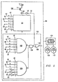
- a test model 98 that includes the logic cell 10 of FIGURE 1 with an auxiliary test circuit 100 is illustrated.
- the test model 98 is used by an automatic test pattern generator (ATPG) 124 for generating a first test vector 120 and a second test vector 122.
- the first test vector is configured to provide an optimal discharge of all nodes in the logic cell 10.
- the second test vector 122 is configured to provide an optimal charge sharing state for the logic cell 10.
- the optimal discharge and charging states are the maximum discharge and charging states, respectively. However, if due to design of the integrated circuit, the maximum states are not justifiable, then the optimal states are the maximum obtainable or substantially the maximum obtainable states.
- the auxiliary test circuit 100 includes a first AND gate 102, a second AND gate 104, a third AND gate 106, an OR gate 108 and a boundary output 130.
- the automatic test pattern generator 124 may be any suitable test pattern generator for generating test vectors for integrated circuit testing including commercially available integrated circuit automatic test pattern generators.
- Test model 98 may be data or software stored on a computer readable medium and used for input to ATPG 124.
- Test model 98 is presented to automatic test pattern generator 124 for generation of appropriate test vectors to verify the operational integrity of logic cell 10.
- logic cell 10 is part of a large integrated circuit
- a modified version of the circuit consisting of test models of logic cells is presented to the automatic test pattern generator 124.
- the output test vectors are input into the integrated circuit inputs and are configured to provide the appropriate input at the logic cell 10.
- the integrated circuit inputs are processed by the integrated circuit and configured to generate the appropriate inputs at the logic cell 10.
- input signals 40 are separately illustrated as providing input signals to transistor network 16, first AND gate 102, and second AND gate 104. However, input signals 40 are provided via a common input signal source. Input signals 40 that provide the input signals for transistor network 16 are fed directly to first AND gate 102. Input signals 40 of transistors in transistor network 16 that have sources connected to ground are inverted and fed into second AND gate 104. The inputs of the remaining transistors in transistor network 16 are fed directly to second AND gate 104. In the exemplary embodiment, input A 42, input C 46, and input F 52 are inverted and fed to second AND gate 104 since transistor A 22, transistor C 26, and transistor F 32 are all connected to ground 34. Input B 44, input D 48 and input E 50 are fed directly to second AND gate 104.
- the test model 98 is used for generating a first test vector 120 and a second test vector 122. This configuration allows for testing with maximum discharge and maximum charge sharing inputs, respectively. The inputs may be suitably modified to account for the maximum obtainable state of the vectors.
- test model 98 is input to an automatic test pattern generator 124 and the falling transition fault on the output of first AND gate 102 is targeted for test vector generation.
- Generation of a test for the falling transition fault provides for a logic level 1 on the output of first AND gate 102 during the first test vector 120.
- all input signals 40 are a logic level 1.
- Providing a logic level 1 for all input signals 40 leads to discharging of all intermediate nodes in logic cell 10 since all paths to ground 34 are connected.
- O node 60, X node 62, Y node 64, and Z node 66 are all discharged.
- the second test vector 122 generated by the automatic test pattern generator 124 provides for a logic level 1 on the output of second AND gate 104. To accomplish this, the input signals 40 for transistors that have sources connected to ground are set a logic level 0, and the remaining input signals 40 are set to a logic level 1.
- the second test vector 122 ensures that no direct path to ground is available thereby evoking the worst case charge sharing behavior for the logic cell 10. Since logic cell 10 does not provide a direct path to ground for any signal path, the second test vector 122 insures observability of any charge sharing and evokes the worst charge sharing behavior for logic cell 10. If any element in the additional circuitry added to minimize charge sharing exhibits a fault, the second test vector 122 insures observability of that fault thereby providing a test for the additional circuitry.
- first AND gate 102 and second AND gate 104 are complementary, the output of third AND gate 106 should always be a logic level 0. Since the output of third AND gate 106 is a logic level 0, the output of OR gate 108 is equal to logic cell output 20 and provides a boundary output 130 for verifying the result of first test vector 120 and second test vector 122.
- the generation of the first test vector 120 and the second test vector 122 for the falling transition fault of the output of first AND gate 102 provides a stuck-at-1 fault test on the output of first AND gate 102 at boundary output 130 on the second test vector 122.
- a stuck-at-0 fault test on O node 60 may be observed on the second test vector 124.
- First test vector 120 initializes logic cell 10 in preparation for the falling transition fault test of second test vector 122.
- the generated test vectors automatically evoke the worst charge sharing behavior, and if charge sharing changes the O node 60 voltage to a logic level 0 on the second test vector, the charge sharing effect is observed at boundary output 130.
- the auxiliary test circuit 100 is only added to test model 98. It is not added to the actual integrated circuit. It is added only to the test model 98 that is given to the automatic test pattern generator 124 such that appropriate test vectors 120 and 122 can be generated.
- a flow diagram illustrates a method for generating test vectors in accordance with one embodiment of the present invention.
- the method commences at step 200 where all logic cell 10 transistor inputs are ANDed together to generate a first intermediate output.
- input: signals 40 are fed to first AND gate 102 to generate the first intermediate output on the output of first AND gate 102.
- step 202 inverts of the inputs to transistors, whose sources are grounded, are ANDed together with the remaining logic cell transistor inputs to generate a second intermediate output.
- transistor A 22, transistor C 46, and transistor F 52 are all coupled to ground 34 and are thus inverted and fed to second AND gate 104.
- transistor B 44, transistor D 48, and transistor E 50 are fed directly to second AND gate 104.
- Second AND gate 104 generates the second intermediate output on the output of second AND gate 104.
- step 204 the first intermediate output and the second intermediate output are ANDed together to generate a third intermediate output.
- the output of first AND gate 102 and the output of second AND gate 104 are fed to third AND gate 106 to generate the third intermediate output on the output of third AND gate 106.
- step 206 the third intermediate output is ORed with an output of the logic cell to generate a primary output.
- the output of third AND gate 106 is fed to OR gate 108, and logic cell output 20 is fed to OR gate 108 to generate boundary output 130.
- Steps 200 through 206 represent the auxiliary test circuit 100 of FIGURE 2.
- test model 98 is forwarded to automatic test pattern generator 124 that then determines a first test vector 120 for the logic cell transistor inputs 40 that cause the first intermediate output to be a logic level 1.
- the first intermediate output is the output of first AND gate 102.
- step 210 the automatic test pattern generator 124 determines a second test vector 122 for the logic cell transistor inputs 40 that cause the first intermediate output to transition to a logic level 0.
Landscapes
- Engineering & Computer Science (AREA)
- General Engineering & Computer Science (AREA)
- Physics & Mathematics (AREA)
- General Physics & Mathematics (AREA)
- Tests Of Electronic Circuits (AREA)
Abstract
Description
Claims (13)
- A method for generating charge sharing test vectors for a circuit, comprising:providing an automatic test pattern generator operable to generate a first test vector and a second test vector;providing a test model including a logic cell of a circuit and an auxiliary test circuit, the auxiliary test circuit including a discharge AND gate and a charge sharing AND gate;selecting an output of the discharge AND gate as a target for a falling transition fault test vector generation by the automatic test pattern generator;generating a first test vector for the test model using the automatic test pattern generator, the first test vector providing an input pattern to discharge nodes of the logic cell, the discharge AND gate evaluating to a logic level 1 for the first test vector;generating a second test vector for the test model using the automatic test pattern generator, the second test vector providing an input pattern to evoke the worst charge sharing behavior for the circuit, the charge sharing AND gate evaluating to a logic level 1 for the second test vector.
- A method for generating charge sharing test vectors for a circuit, comprising:providing an automatic test pattern generator operable to generate a first test vector and a second test vector;providing a test model including a logic cell of a circuit and an auxiliary test circuit;setting inputs for all sources of the logic cell to a logic level 1, the input values providing an input pattern for the automatic test pattern generator;generating a first test vector for the test model using the automatic test pattern generator, the first test vector providing an input pattern to discharge nodes of the logic cell;setting inputs for sources of the circuit connected to ground to a logic level 0;setting inputs for sources of the circuit not connected to ground to a logic level 1;generating a second test vector for the test model using the automatic test pattern generator, the second test vector providing an input pattern to evoke the worst charge sharing behavior for the circuit.
- The method of Claim 2, wherein the logic cell is a domino circuit.
- The method of Claim 2, wherein the logic cell is a dynamic circuit.
- The method of Claim 2, wherein the auxiliary test circuit includes a first AND gate, a second AND gate, a third AND gate, and an OR gate.
- The method of Claim 5, further comprising: targeting an output of the first AND gate for a falling transition fault test vector generation by the automatic test pattern generator.
- A method for charge sharing testing of circuits, comprising:precharging an output node to a logic level 1;setting source inputs to values such that a path to ground is provided for source components associated with the source inputs;discharging source components of the circuit;precharging the output node to a logic level 1;setting source inputs to values such that sources coupled to ground are a logic level 0 and that other sources are a logic level 1;evaluating the output node value;generating an error condition in response to the output node value evaluating to a logic level 0 indicating a charge sharing error.
- A method for generating test vectors for a charge sharing corrective circuit to a logic cell, comprising:ANDing all logic cell transistor inputs together to generate a first intermediate output;ANDing inverted grounded logic cell transistor inputs together with the remaining logic cell transistor inputs to generate a second intermediate output;ANDing the first and second intermediate outputs together to generate a third intermediate output;ORing the third intermediate output with an output of the logic cell to generate a primary output;determining a first test vector for the logic cell transistor inputs that cause the first intermediate output to be a logic level 1; anddetermining a second test vector for the logic cell transistor inputs that causes the first intermediate output to transition to a logic level 0.
- A method for testing a logic cell, comprising:applying a first test vector to a logic cell, the first test vector operable to optimize discharge of nodes in the logic cell;applying a second test vector to the logic cell, the second test vector operable to optimize charge sharing between nodes in the logic cell; andmeasuring a primary output from the logic cell to determine a fault status of a charge sharing corrective circuit for the cell.
- The method of Claim 9, the first test vector operable to maximize discharge of nodes in the logic cell.
- The method of Claim 9, the second test vector operable to maximize charge sharing between nodes in the logic cell.
- The method of Claim 9, further comprising:generating a first integrated circuit vector;applying the first integrated circuit vector to an integrated circuit including the logic cell; andthe integrated circuit processing the first integrated circuit vector to generate the first test vector at the logic cell.
- The method of Claim 12, further comprising:generating a second integrated circuit vector;applying the second integrated circuit vector to the integrated circuit including the logic cell;the integrated circuit processing the second integrated circuit vector to generate the second test vector at the logic cell; andmeasuring a primary output from the integrated circuit to determine the fault status of the charge sharing corrective circuit for the cell.
Applications Claiming Priority (4)
| Application Number | Priority Date | Filing Date | Title |
|---|---|---|---|
| US17931400P | 2000-01-31 | 2000-01-31 | |
| US179314P | 2000-01-31 | ||
| US09/713,416 US6553547B1 (en) | 2000-01-31 | 2000-11-15 | Method and system for generating charge sharing test vectors |
| US713416 | 2000-11-15 |
Publications (3)
| Publication Number | Publication Date |
|---|---|
| EP1122547A2 true EP1122547A2 (en) | 2001-08-08 |
| EP1122547A3 EP1122547A3 (en) | 2003-08-13 |
| EP1122547B1 EP1122547B1 (en) | 2005-10-26 |
Family
ID=26875213
Family Applications (1)
| Application Number | Title | Priority Date | Filing Date |
|---|---|---|---|
| EP01200354A Expired - Lifetime EP1122547B1 (en) | 2000-01-31 | 2001-01-31 | Method and system for generating charge sharing test vectors |
Country Status (3)
| Country | Link |
|---|---|
| US (1) | US6553547B1 (en) |
| EP (1) | EP1122547B1 (en) |
| DE (1) | DE60114259T2 (en) |
Families Citing this family (2)
| Publication number | Priority date | Publication date | Assignee | Title |
|---|---|---|---|---|
| US8386866B2 (en) * | 2010-08-17 | 2013-02-26 | Eigenix | Methods for implementing variable speed scan testing |
| US9513330B2 (en) * | 2012-06-29 | 2016-12-06 | Intel Corporation | Charge sharing testing of through-body-vias |
Family Cites Families (4)
| Publication number | Priority date | Publication date | Assignee | Title |
|---|---|---|---|---|
| US5831990A (en) * | 1996-06-19 | 1998-11-03 | Hewlett-Packard Company | Test-mode control for dynamic logic gates |
| US6094734A (en) * | 1997-08-22 | 2000-07-25 | Micron Technology, Inc. | Test arrangement for memory devices using a dynamic row for creating test data |
| US6415405B1 (en) * | 1998-10-27 | 2002-07-02 | Intrinsity, Inc. | Method and apparatus for scan of synchronized dynamic logic using embedded scan gates |
| US6292818B1 (en) * | 1999-01-12 | 2001-09-18 | Hewlett-Packard Company | Method and apparatus for performing a sum-and-compare operation |
-
2000
- 2000-11-15 US US09/713,416 patent/US6553547B1/en not_active Expired - Lifetime
-
2001
- 2001-01-31 EP EP01200354A patent/EP1122547B1/en not_active Expired - Lifetime
- 2001-01-31 DE DE60114259T patent/DE60114259T2/en not_active Expired - Lifetime
Also Published As
| Publication number | Publication date |
|---|---|
| EP1122547B1 (en) | 2005-10-26 |
| US6553547B1 (en) | 2003-04-22 |
| EP1122547A3 (en) | 2003-08-13 |
| DE60114259D1 (en) | 2005-12-01 |
| DE60114259T2 (en) | 2006-07-13 |
Similar Documents
| Publication | Publication Date | Title |
|---|---|---|
| US10802077B1 (en) | Test circuit for dynamic checking for faults on functional and BIST clock paths to memory in both ATPG and LBIST modes | |
| Saikiran et al. | Robust built-in defect-detection for low drop-out regulators using digital mismatch injection | |
| Bose et al. | A fault simulator for MOS LSI circuits | |
| US7269772B1 (en) | Method and apparatus for built-in self-test (BIST) of integrated circuit device | |
| US6553547B1 (en) | Method and system for generating charge sharing test vectors | |
| US7202688B2 (en) | Output buffer circuit having signal path used for testing and integrated circuit and test method including the same | |
| US7137050B2 (en) | Compression circuit for testing a memory device | |
| US5857164A (en) | System for calculating current consumption characteristics of cells | |
| Liao et al. | Optimal voltage testing for physically-based faults | |
| JP4749754B2 (en) | Test apparatus and test method | |
| JP4263374B2 (en) | Semiconductor integrated circuit | |
| Hosokawa et al. | A low power oriented multiple target test generation method for 2-cycle gate-exhaustive faults | |
| US7332938B2 (en) | Domino logic testing systems and methods | |
| US5381418A (en) | Testable latch self checker | |
| Pomeranz et al. | Location of stuck-at faults and bridging faults based on circuit partitioning | |
| US5444391A (en) | Tie-up and tie-down circuits with a primary input for testability improvement of logic networks | |
| Ahlawat et al. | A low cost technique for scan chain diagnosis | |
| JP2005037126A (en) | Charge dispersion test vector generation method and system | |
| JP3025476B2 (en) | Semiconductor integrated circuit | |
| US5130575A (en) | Testable latch self checker | |
| US20250389767A1 (en) | Voltage drop detection in a power grid on an integrated circuit | |
| JP2000258503A (en) | Output current measurement method | |
| US6850075B1 (en) | SRAM self-timed write stress test mode | |
| Samala | Test Pattern Generation for Double Transition Faults | |
| Gruetzner et al. | Simulation and test of faults in WSI interconnect systems |
Legal Events
| Date | Code | Title | Description |
|---|---|---|---|
| PUAI | Public reference made under article 153(3) epc to a published international application that has entered the european phase |
Free format text: ORIGINAL CODE: 0009012 |
|
| AK | Designated contracting states |
Kind code of ref document: A2 Designated state(s): AT BE CH CY DE DK ES FI FR GB GR IE IT LI LU MC NL PT SE TR |
|
| AX | Request for extension of the european patent |
Free format text: AL;LT;LV;MK;RO;SI |
|
| PUAL | Search report despatched |
Free format text: ORIGINAL CODE: 0009013 |
|
| AK | Designated contracting states |
Designated state(s): AT BE CH CY DE DK ES FI FR GB GR IE IT LI LU MC NL PT SE TR |
|
| AX | Request for extension of the european patent |
Extension state: AL LT LV MK RO SI |
|
| 17P | Request for examination filed |
Effective date: 20040213 |
|
| AKX | Designation fees paid |
Designated state(s): DE FR GB |
|
| 17Q | First examination report despatched |
Effective date: 20040406 |
|
| GRAP | Despatch of communication of intention to grant a patent |
Free format text: ORIGINAL CODE: EPIDOSNIGR1 |
|
| GRAS | Grant fee paid |
Free format text: ORIGINAL CODE: EPIDOSNIGR3 |
|
| GRAA | (expected) grant |
Free format text: ORIGINAL CODE: 0009210 |
|
| AK | Designated contracting states |
Kind code of ref document: B1 Designated state(s): DE FR GB |
|
| REG | Reference to a national code |
Ref country code: GB Ref legal event code: FG4D |
|
| REF | Corresponds to: |
Ref document number: 60114259 Country of ref document: DE Date of ref document: 20051201 Kind code of ref document: P |
|
| ET | Fr: translation filed | ||
| PLBE | No opposition filed within time limit |
Free format text: ORIGINAL CODE: 0009261 |
|
| STAA | Information on the status of an ep patent application or granted ep patent |
Free format text: STATUS: NO OPPOSITION FILED WITHIN TIME LIMIT |
|
| 26N | No opposition filed |
Effective date: 20060727 |
|
| REG | Reference to a national code |
Ref country code: FR Ref legal event code: PLFP Year of fee payment: 16 |
|
| PGFP | Annual fee paid to national office [announced via postgrant information from national office to epo] |
Ref country code: GB Payment date: 20151230 Year of fee payment: 16 |
|
| PGFP | Annual fee paid to national office [announced via postgrant information from national office to epo] |
Ref country code: DE Payment date: 20160127 Year of fee payment: 16 |
|
| PGFP | Annual fee paid to national office [announced via postgrant information from national office to epo] |
Ref country code: FR Payment date: 20151230 Year of fee payment: 16 |
|
| REG | Reference to a national code |
Ref country code: DE Ref legal event code: R119 Ref document number: 60114259 Country of ref document: DE |
|
| GBPC | Gb: european patent ceased through non-payment of renewal fee |
Effective date: 20170131 |
|
| REG | Reference to a national code |
Ref country code: FR Ref legal event code: ST Effective date: 20170929 |
|
| PG25 | Lapsed in a contracting state [announced via postgrant information from national office to epo] |
Ref country code: FR Free format text: LAPSE BECAUSE OF NON-PAYMENT OF DUE FEES Effective date: 20170131 |
|
| PG25 | Lapsed in a contracting state [announced via postgrant information from national office to epo] |
Ref country code: GB Free format text: LAPSE BECAUSE OF NON-PAYMENT OF DUE FEES Effective date: 20170131 Ref country code: DE Free format text: LAPSE BECAUSE OF NON-PAYMENT OF DUE FEES Effective date: 20170801 |