EP1122332A1 - Method and apparatus for deposition of low residual halogen content TiN film - Google Patents
Method and apparatus for deposition of low residual halogen content TiN film Download PDFInfo
- Publication number
- EP1122332A1 EP1122332A1 EP01300949A EP01300949A EP1122332A1 EP 1122332 A1 EP1122332 A1 EP 1122332A1 EP 01300949 A EP01300949 A EP 01300949A EP 01300949 A EP01300949 A EP 01300949A EP 1122332 A1 EP1122332 A1 EP 1122332A1
- Authority
- EP
- European Patent Office
- Prior art keywords
- tin
- layer
- film
- halogen
- thickness
- Prior art date
- Legal status (The legal status is an assumption and is not a legal conclusion. Google has not performed a legal analysis and makes no representation as to the accuracy of the status listed.)
- Withdrawn
Links
Images


Classifications
-
- H—ELECTRICITY
- H10—SEMICONDUCTOR DEVICES; ELECTRIC SOLID-STATE DEVICES NOT OTHERWISE PROVIDED FOR
- H10P—GENERIC PROCESSES OR APPARATUS FOR THE MANUFACTURE OR TREATMENT OF DEVICES COVERED BY CLASS H10
- H10P14/00—Formation of materials, e.g. in the shape of layers or pillars
- H10P14/40—Formation of materials, e.g. in the shape of layers or pillars of conductive or resistive materials
- H10P14/418—Formation of materials, e.g. in the shape of layers or pillars of conductive or resistive materials the conductive layers comprising transition metals
-
- C—CHEMISTRY; METALLURGY
- C23—COATING METALLIC MATERIAL; COATING MATERIAL WITH METALLIC MATERIAL; CHEMICAL SURFACE TREATMENT; DIFFUSION TREATMENT OF METALLIC MATERIAL; COATING BY VACUUM EVAPORATION, BY SPUTTERING, BY ION IMPLANTATION OR BY CHEMICAL VAPOUR DEPOSITION, IN GENERAL; INHIBITING CORROSION OF METALLIC MATERIAL OR INCRUSTATION IN GENERAL
- C23C—COATING METALLIC MATERIAL; COATING MATERIAL WITH METALLIC MATERIAL; SURFACE TREATMENT OF METALLIC MATERIAL BY DIFFUSION INTO THE SURFACE, BY CHEMICAL CONVERSION OR SUBSTITUTION; COATING BY VACUUM EVAPORATION, BY SPUTTERING, BY ION IMPLANTATION OR BY CHEMICAL VAPOUR DEPOSITION, IN GENERAL
- C23C16/00—Chemical coating by decomposition of gaseous compounds, without leaving reaction products of surface material in the coating, i.e. chemical vapour deposition [CVD] processes
- C23C16/22—Chemical coating by decomposition of gaseous compounds, without leaving reaction products of surface material in the coating, i.e. chemical vapour deposition [CVD] processes characterised by the deposition of inorganic material, other than metallic material
- C23C16/30—Deposition of compounds, mixtures or solid solutions, e.g. borides, carbides, nitrides
- C23C16/34—Nitrides
-
- C—CHEMISTRY; METALLURGY
- C23—COATING METALLIC MATERIAL; COATING MATERIAL WITH METALLIC MATERIAL; CHEMICAL SURFACE TREATMENT; DIFFUSION TREATMENT OF METALLIC MATERIAL; COATING BY VACUUM EVAPORATION, BY SPUTTERING, BY ION IMPLANTATION OR BY CHEMICAL VAPOUR DEPOSITION, IN GENERAL; INHIBITING CORROSION OF METALLIC MATERIAL OR INCRUSTATION IN GENERAL
- C23C—COATING METALLIC MATERIAL; COATING MATERIAL WITH METALLIC MATERIAL; SURFACE TREATMENT OF METALLIC MATERIAL BY DIFFUSION INTO THE SURFACE, BY CHEMICAL CONVERSION OR SUBSTITUTION; COATING BY VACUUM EVAPORATION, BY SPUTTERING, BY ION IMPLANTATION OR BY CHEMICAL VAPOUR DEPOSITION, IN GENERAL
- C23C16/00—Chemical coating by decomposition of gaseous compounds, without leaving reaction products of surface material in the coating, i.e. chemical vapour deposition [CVD] processes
- C23C16/56—After-treatment
Definitions
- the present invention relates to a method and apparatus for producing thick titanium nitride film for plug-fill type applications. More specifically, the present invention relates to a method for producing TiN depositions having a thickness of about 400 ⁇ or more (and typically 1000 ⁇ or more), where the deposited material maintains low resistivity, low stress, and low chlorine content.
- Titanium nitride layers have been used in semiconductor device structures as barrier layers for preventing the interdiffusion of adjacent layers of materials such as aluminum and silicon, for example.
- the resistivity of a conventional titanium nitride film is frequently greater than 150 ⁇ cm, which detracts from the overall conductivity of the layered conductive structure to which it contributes.
- high residual film stress can cause a titanium nitride film to peel off from the surface of an underlying layer (typically silicon oxide, titanium, or titanium silicide). In the alternative, if the film does not peel off, the film stress can cause feature distortion on the substrate (typically a silicon wafer) surface or even deformation of a thin wafer.
- U.S. Patent No. 4,570,328 to Price et al. issued on February 18, 1986 describes a method of producing titanium nitride MOS device gate electrodes.
- the gate electrode and interconnect are fabricated from low pressure chemical vapor deposited titanium nitride.
- the film thicknesses described are between about 100nm and 200 nm (1,000 ⁇ and 2,000 ⁇ ).
- the films are deposited from a feed gas of titanium tetrachloride, ammonia and hydrogen, at temperatures between about 680 °C and 800 °C and at a pressure ranging between 100 mTorr and 300 mTorr.
- the films are subsequently annealed in a nitrogen atmosphere at a temperature between 900 °C and 1,000 °C, to reduce resistivity.
- Price et al. explains that at film formation temperatures greater than approximately 800 °C, severe gas phase depletion occurs resulting in a loss of control of the film thickness' uniformity.
- temperatures less than approximately 680 °C TiNCl x is grown instead of the desired TiN, and annealing of the film causes 'cracks' and 'blisters' that form when chlorine atoms escape the film.
- halogen-comprising typically chlorine-comprising residues from TiN films deposited using CVD.
- the residual halogen content increases resistivity and can cause damage to the film structure during subsequent processing at elevated temperatures.
- a method of removing halogen-comprising residues from a thick TiN film where the method has minimal effect on the final film structure while providing a film having a low resistivity, preferably less than about 175 ⁇ cm.
- a method for producing a substantially uniform TiN film of a thickness of 400 ⁇ or higher, preferably 1,000 ⁇ or higher, where the resistivity of the deposited film is less than about 175 ⁇ cm.
- the method comprises forming a layer of TiN having a thickness of 400 ⁇ or less by chemical vapor deposition using a halogen-comprising precursor and a nitrogen-comprising precursor; a halogen residue removal step which includes annealing the layer of TiN film in the presence of at least one gas which reacts with the halogen to produce a reaction product which is volatile under the precessing conditions; and, repeating the film forming and halogen residue removal steps multiple times, to form a multi-layer TiN film having the desired thickness.
- the halogen residue removal step is carried out in the chemical vapor deposition chamber used for deposition of the TiN film, so that a series of TiN deposition and halogen removal steps can be carried out rapidly.
- the use of a series of deposition-anneal steps provides for a more complete removal of halogen residues from the thick titanium nitride film while permitting a rapid film deposition rate.
- the residual halogen content in the TiN film produced by the method of the invention is less than about 1.5 atomic percent, and the film is free from blisters and cracks.
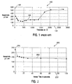
- Figure 1 graphically illustrates the relationship between film thickness and resistivity in a TiN film of made according to the prior art, using a continuous deposition process. This figure shows that resistivity increases to about 520 ⁇ cm as the film thickness approaches 2800 ⁇ .
- Figure 2 graphically illustrates the relationship between the resistivity and annealing time for a typical prior art TiN film deposited in a single deposition step and having a thickness of 200 ⁇ . No change in film thickness was observed during annealing.
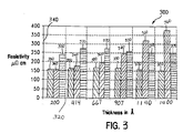
- Figure 3 is a bar graph which depicts a comparison of the relationship between resistivity and film thickness for films deposited by different methods.
- the total film thickness is shown on scale 320.
- the resistivity is shown on scale 340.
- the bar labeled 350 represents a film deposited in multiple steps (with the exception of the 200 ⁇ thickness), where multiple layers averaging approximately 245 ⁇ were deposited to reach the total film thickness indicated. After each layer deposition, the film(with substrate) was annealed in the presence of an ammonia-comprising ambient.
- the bar labeled 360 represents a film deposited in a single deposition, where the film was annealed in the presence of an ammonia-comprising ambient.
- the bar labeled 370 represents a film deposited in a single deposition which was not annealed.
- Figure 4 is a schematic representation of a prior art CVD chamber of the kind which can be used to practice the present invention.
- Figure 5 is a schematic representation of an apparatus for practicing the present invention which includes elements for computerized control of the apparatus used to carry out the method of the invention.
- the present invention relates to method for depositing thick titanium nitride films (having a film thickness greater than about 400 ⁇ ), where the resistivity of the deposited film is less than about 175 ⁇ cm, and the residual halogen content is less than 1.5 atomic percent.
- the method can be used to produce a substantially uniform TiN film of a thickness of 1000 ⁇ or higher, where the film deposition rate is at least 400 ⁇ /min and the resistivity of the deposited film is less than about 175 ⁇ cm.
- process chamber 400 includes an interior chamber 450 which is essentially bucket shaped, having a cylindrical sidewall 454 and a base 452. Interior to sidewall 454 is a heated liner 462. There is an opening 456 in one portion of sidewall 454, which is connected to an exhaust assembly (not shown) for the removal of process and product gases.
- the chamber base 452 has a centrally-located opening 458, which is provided to accommodate a pedestal assembly 460 which is attached to substrate support pedestal 474, which typically supports a semiconductor wafer for processing.
- Substrate lift pins 478 operate to lower and raise a substrate (not shown) to the upper surface of support pedestal 474.
- a resistive heater 464 is used to maintain heated liner 462 at a desired temperature.
- Power to resistive heater 464 is controlled based on information provided from thermocouple 466 embedded in heated liner 462.
- Process gases enter process chamber 400 through a gas distribution manifold 476, which is connected to a dual-gas showerhead assembly 468 and pass through a faceplate 470 to reach processing area 472.
- the showerhead assembly 468 provides a dual-gas separate entry for TiCl 4 and NH 3 into the processing area 472 without premixing of the gases.
- the gas distribution manifold assembly 476 also serves as the lid of process chamber 400. To avoid the formation of undesirable deposits inside the showerhead assembly 468, separate flow paths or passageways are established through different channels (not shown) in showerhead assembly 468.
- FIG. 5 shows a computer 500.
- Computer 500 comprises a processor 502, memory 504 adapted to store instructions 506, and one or more ports 508.
- Processor 502 is adapted to communicate with memory 504 and to execute instructions 506.
- Processor 502 and memory 504 are also adapted to communicate with one or more ports 508.
- Ports 508 are adapted to communicate with a CVD/Treatment chamber 512. Chamber 512 is adapted to carry out process steps in accordance with signals received from processor 502 via ports 508.
- computer 502 can control the composition and feed rate of the CVD process gases, the composition and geed rate of the residual halogen removal treatment gases, the process temperature, the pressure in the chamber, the time period for each process step, and other similar functions.
- computer 502 is adapted to receive measurements that describe the condition in the chamber, and adapt the process variables accordingly. This programmed control of process variables enables production of a predetermined device etch profile as required for a given use application.
- titanium nitride film is deposited by introducing titanium tetrahalide (typically, titanium tetrachloride), and ammonia into a reaction chamber.
- the gases react to form titanium nitride according to the following general reaction: 6TiX 4 + 8NH 3 ⁇ 6TiN + N 2 + 24 HX Wherein X is a halogen atom.
- the halogen atom is chlorine, but the present invention is not intended to be limited to the use of a chlorine-comprising halogen precursor. In practice, however, the reaction does not yield 100 % product, and depending on the processing conditions, some halogen atoms are often trapped within the resulting TiN film.
- the residual halogen atoms cause several problems. For example, the presence of residual chlorine in the TiN film increases the risk of corroding adjacent conductive layers, as the chlorine migrates into these layer. In addition, the residual chlorine atoms generally increase the film's resistivity. In addition, Applicants discovered if a very thick film (1,000 ⁇ or greater) is annealed in the presence of NH 3 , the residual halogen atoms will cause the film to form micro cracks. However, applicants discovered that annealing can be carried out without causing such cracks to form if the thickness of the film being annealed does not exceed 400 ⁇ .
- graph 100 illustrates the prior art relationship between the resistivity (measured in ⁇ cm), shown on the graph 100 ordinate 140, and the film thickness of a TiN film (measured in ⁇ ), shown on graph 100 abscissa 120.
- Curve 160 illustrates that for a TiN film made using a continuous deposition process, the resistivity of a film tends to decrease with film thickness up to about 400 ⁇ . As film thickness continues to increase, resistivity begins to increase, making a substantial increase at film thicknesses over about 1,350 ⁇ .
- FIG. 2 shows graph 200, which illustrates he effect on film resistivity of annealing a 200 ⁇ thick TiN film, when the film is annealed at approximately 680°C, in the presence of NH 3 , at a pressure of about 10 Torr.
- the resistivity is shown on the ordinate 340 in ⁇ cm, and the annealing time in seconds is shown on the abscissa 320.
- a treatment time of about 20 seconds may be used to achieve excellent results.
- Figure 3 provides comparative data which illustrates the advantages of Applicants' invention.
- Bar Graph 300 shows comparative data for TiN films deposited using three different methods. The TiN film thickness in ⁇ is shown on scale 320, while the film resistivity in ⁇ ⁇ cm is shown on scale 340.
- Films of various thicknesses which were CVD deposited using the prior art continuous deposition method and annealed in the presence of NH 3 after completion of deposition are represented by bars labeled 360.
- the annealing was carried out at about 680 °C in the presence of NH 3 , at a pressure of about 10 Torr.
- Films of various thicknesses deposited using the method of the present invention are represented on Bar Graph 300 by bars labeled 350. These films were CVD deposited in a series of deposition/anneal steps, where each step included CVD deposition of a layer of TiN, followed by annealing in the presence of NH 3 . The average thickness of an individual film layer CVD deposition was about 240 ⁇ . (The technique used to CVD deposit all of the films is shown on Bar Graph 300 is described in the Example below.) After each CVD deposition of an individual film layer, the TiN film (which increased in thickness after deposition of each layer) was annealed in the presence of NH 3 at about 680 °C, at a pressure of 10 Torr for about 20 seconds. A longer annealing time may be used if desired, but is not necessary in view of the data presented in Figure 2. The number of steps performed depended on the final thickness of the film produced.
- the resistivity of a 1,400 ⁇ thick film produced by the method of the invention is only about 150 ⁇ cm, which is essentially the same as the resistivity of a 200 ⁇ thick film annealed in the presence of NH 3 .
- the resistivity of a 1,400 ⁇ thick film increased to about 375 ⁇ cm, compared with 150 ⁇ cm for a 200 ⁇ thick film.
- TiSi titanium silicide
- the substrate described above was placed in the TxZ- I TM CVD chamber previously described.
- the TiN layer may be CVD deposited on a substrate heated to a temperature ranging from about 550 °C to a temperature of about 720 °C.
- the TiN layers were CVD deposited at about 680 °C.
- the process chamber was heated to about 680 °C over a time period of about 20 seconds. Thereafter, titanium tetrachloride (which is vaporized prior to entering the process chamber) and process gases including ammonia, nitrogen, helium and argon, were introduced into the process chamber.
- titanium tetrachloride (TiCl 4 ) entering the process chamber ranges from about 50 mg/min. to about 400 mg/min.
- the typical flow rate ranges for the process gases are: ammonia (NH 3 ) from about 50 sccm to about 200 sccm; nitrogen (N 2 ) from about 500 sccm to about 2,000 sccm; helium (He) from about 500 sccm to about 2, 000 sccm; and, argon (Ar) from about 500 sccm to about 2,000 sccm.
- the process chamber pressure typically ranges between about 5 Torr and about 30 Torr.
- the feed rate for TiCl 4 was 200 mg/min.; and, the process gas flow rates were 100 sccm NH 2 ; 1,000 sccm N 2 ; 1,000 sccm He; and 1,000 sccm Ar.
- the CVD process chamber pressure was 10 Torr throughout each film deposition step.
- the combination of gases, including vaporized TiCl 4 was fed into chamber 400 through gas distribution manifold 476, and was mixed through a face plate (not shown) on showerhead 468.
- the pressure in the process chamber was maintained at 10 Torr, with excess product and process gas being exhausted through opening 456 in the chamber wall, leading to an exhaust assembly (not shown).
- the flow of TiCl 4 was stopped after about 20 seconds. Thicker films required a proportional increase in TiCl 4 feed time. After the deposition step was completed, the films were treated for chlorine removal (with the exception of films shown in Bar Graph 300 as bars 370, which were not annealed or treated for chlorine removal).
- the substrate, including the TiN film temperature was maintained at about 680 °C and the following process gases were fed to the process chamber to produce the ambient for chlorine removal from the deposited film.
- the typical flow rate ranges for the chlorine treatment process gases are: ammonia (NH 3 ) from about 100 sccm to about 3000 sccm; nitrogen (N 2 ) from about 500 sccm to about 2,000 sccm; helium (He) from about 500 sccm to about 2, 000 sccm; and, argon (Ar) from about 500 sccm to about 2,000 sccm.
- the feed rate for NH 2 was 500 sccm; N 2 was 1,000 sccm; He was 1,000 sccm, and Ar was 1,000 sccm.
- the chlorine removal treatment gases were fed into the CVD process chamber through the same inlet system as previously mentioned, with chamber pressure being maintained at a pressure ranging from about 5 to about 30 Torr in the manner previously described. Preferably the chamber pressure was about the same as the pressure used during CVD of the TiN film.
- the residual chlorine removal treatment step was carried on for a time period ranging from about 5 to about 40 seconds, preferably for about 20 seconds. The number of residual chlorine treatments depended on the number of TiN layer CVD depositions.
- the films shown in bars labeled 360 on Bar Graph 300 deposited in one continuous deposition and were treated only once, at the end of the deposition.
- the films shown in bars labeled 350 were deposited using multiple deposition/anneal steps, wherein the average individual film layer CVD deposition thickness was about 240 ⁇ , with a chlorine removal treatment step occurring after each CVD deposition.
Landscapes
- Chemical & Material Sciences (AREA)
- General Chemical & Material Sciences (AREA)
- Chemical Kinetics & Catalysis (AREA)
- Engineering & Computer Science (AREA)
- Materials Engineering (AREA)
- Mechanical Engineering (AREA)
- Metallurgy (AREA)
- Organic Chemistry (AREA)
- Inorganic Chemistry (AREA)
- Chemical Vapour Deposition (AREA)
- Electrodes Of Semiconductors (AREA)
Abstract
The present disclosure pertains to the discovery that TiN films having a
thickness of greater than about 400 Å and, particularly greater than 1000 Å, and a
resistivity of less than about 175 µΩcm, can be produced by a CVD technique in
which a series of TiN layers are deposited to form a desired TiN film thickness. Each
layer is deposited employing a CVD deposition /treatment step. During a treatment
step, residual halogen (typically chlorine) was removed from the CVD deposited film.
Specifically, a TiN film having a thickness of greater than about 400 Å was prepared
by a multi deposition/treatment step process where individual TiN layers having a
thickness of less than 400 Å were produced in series to provide a finished TiN layer
having a combined desired thickness. Each individual TiN layer was CVD deposited
and then treated by exposing the TiN surface to ammonia in an annealing step carried
out in an ammonia ambient. The TiN film formed in this manner not only had a
resistivity of less than about 175 µΩcm, but was substantially free of micro cracks as
well, including films having a thickness greater than 1,000 Å.
Description
- The present invention relates to a method and apparatus for producing thick titanium nitride film for plug-fill type applications. More specifically, the present invention relates to a method for producing TiN depositions having a thickness of about 400 Å or more (and typically 1000 Å or more), where the deposited material maintains low resistivity, low stress, and low chlorine content.
- Titanium nitride layers have been used in semiconductor device structures as barrier layers for preventing the interdiffusion of adjacent layers of materials such as aluminum and silicon, for example. However, the resistivity of a conventional titanium nitride film is frequently greater than 150 µΩcm, which detracts from the overall conductivity of the layered conductive structure to which it contributes. Further, high residual film stress can cause a titanium nitride film to peel off from the surface of an underlying layer (typically silicon oxide, titanium, or titanium silicide). In the alternative, if the film does not peel off, the film stress can cause feature distortion on the substrate (typically a silicon wafer) surface or even deformation of a thin wafer.
- U.S. Patent No. 5,610,106 to Foster et al., issued on March 11, 1997 and assigned to Sony Corporation, describes TiN films as typically being deposited over a substrate by reactively sputtering titanium in a nitrogen-argon mixture, or by evaporating titanium in a nitrogen atmosphere. The disclosure adds that sputtered films provide poor conformity while chemical vapor deposited films require the use of high temperatures which make the process impractical for use in multi-level metalization schemes. Foster suggests a plasma enhanced CVD process to overcome these deficiencies. The method disclosed by Foster et al. is for the deposition of films having a thickness ranging from about 200 Å to about 500 Å, and the deposition is carried out at a temperature of about 400 °C to about 500 °C and a process chamber pressure of about 5 Torr.
- U.S. Patent Nos. 5,279,857 and 5,308,655 to Eichman et al., issued on January 18, 1994 and May 3, 1994, respectively, describe a method for reducing the chlorine content of TiN films by first forming a TiN film on a wafer, and then reacting the residual chlorine in the film with ammonia at a temperature of 600-700 °C and pressure of 115-300 mTorr to remove the residual chlorine. The theory presented is that low pressure chemical vapor deposition titanium nitride films deposited from TiCl4 and NH3 gas incorporates a large amount of chlorine in the film. This chlorine is said to be found to be concentrated at the grain boundaries and film interfaces. The Eichman et al. patents refer to "thin films" of titanium nitride, but are silent as to the thickness of such a film.
- U.S. Patent No. 4,570,328 to Price et al., issued on February 18, 1986 describes a method of producing titanium nitride MOS device gate electrodes. In particular, the gate electrode and interconnect are fabricated from low pressure chemical vapor deposited titanium nitride. The film thicknesses described are between about 100nm and 200 nm (1,000 Å and 2,000 Å). The films are deposited from a feed gas of titanium tetrachloride, ammonia and hydrogen, at temperatures between about 680 °C and 800 °C and at a pressure ranging between 100 mTorr and 300 mTorr. The films are subsequently annealed in a nitrogen atmosphere at a temperature between 900 °C and 1,000 °C, to reduce resistivity. Price et al. explains that at film formation temperatures greater than approximately 800 °C, severe gas phase depletion occurs resulting in a loss of control of the film thickness' uniformity. At temperatures less than approximately 680 °C, TiNClx is grown instead of the desired TiN, and annealing of the film causes 'cracks' and 'blisters' that form when chlorine atoms escape the film.
- As indicated by the references cited above, there is a need for a method for removing halogen-comprising (typically chlorine-comprising) residues from TiN films deposited using CVD. The residual halogen content increases resistivity and can cause damage to the film structure during subsequent processing at elevated temperatures. There is a particular need for a method of removing halogen-comprising residues from a thick TiN film, where the method has minimal effect on the final film structure while providing a film having a low resistivity, preferably less than about 175 µΩ cm.
- In accordance with the present invention, a method is provided for producing a substantially uniform TiN film of a thickness of 400 Å or higher, preferably 1,000 Å or higher, where the resistivity of the deposited film is less than about 175 µΩcm. The method comprises forming a layer of TiN having a thickness of 400 Å or less by chemical vapor deposition using a halogen-comprising precursor and a nitrogen-comprising precursor; a halogen residue removal step which includes annealing the layer of TiN film in the presence of at least one gas which reacts with the halogen to produce a reaction product which is volatile under the precessing conditions; and, repeating the film forming and halogen residue removal steps multiple times, to form a multi-layer TiN film having the desired thickness. Preferably the halogen residue removal step is carried out in the chemical vapor deposition chamber used for deposition of the TiN film, so that a series of TiN deposition and halogen removal steps can be carried out rapidly. The use of a series of deposition-anneal steps provides for a more complete removal of halogen residues from the thick titanium nitride film while permitting a rapid film deposition rate. Preferably, the residual halogen content in the TiN film produced by the method of the invention is less than about 1.5 atomic percent, and the film is free from blisters and cracks. The following drawings are provided by way of example.
- Figure 1 graphically illustrates the relationship between film thickness and resistivity in a TiN film of made according to the prior art, using a continuous deposition process. This figure shows that resistivity increases to about 520 µΩcm as the film thickness approaches 2800 Å.
- Figure 2 graphically illustrates the relationship between the resistivity and annealing time for a typical prior art TiN film deposited in a single deposition step and having a thickness of 200 Å. No change in film thickness was observed during annealing.
- Figure 3 is a bar graph which depicts a comparison of the relationship between resistivity and film thickness for films deposited by different methods. The total film thickness is shown on
scale 320. The resistivity is shown on scale 340. The bar labeled 350 represents a film deposited in multiple steps (with the exception of the 200 Å thickness), where multiple layers averaging approximately 245 Å were deposited to reach the total film thickness indicated. After each layer deposition, the film(with substrate) was annealed in the presence of an ammonia-comprising ambient. The bar labeled 360 represents a film deposited in a single deposition, where the film was annealed in the presence of an ammonia-comprising ambient. The bar labeled 370 represents a film deposited in a single deposition which was not annealed. - Figure 4 is a schematic representation of a prior art CVD chamber of the kind which can be used to practice the present invention.
- Figure 5 is a schematic representation of an apparatus for practicing the present invention which includes elements for computerized control of the apparatus used to carry out the method of the invention.
- The present invention relates to method for depositing thick titanium nitride films (having a film thickness greater than about 400 Å), where the resistivity of the deposited film is less than about 175 µΩcm, and the residual halogen content is less than 1.5 atomic percent. In a particularly useful instance, the method can be used to produce a substantially uniform TiN film of a thickness of 1000 Å or higher, where the film deposition rate is at least 400 Å/min and the resistivity of the deposited film is less than about 175 µΩcm.
- As a preface to the detailed description, it should be noted that, as used in this specification and the appended claims, the singular forms "a", "an", and "the" include plural referents, unless the context clearly dictates otherwise.
Any conventional apparatus may be used to carry out the present invention. The apparatus which was used by applicants in development of the method of the invention was a TxZ- I™ processing system available from Applied Materials, Inc. of Santa Clara California. The TxZ- I™ processing system is available on both a Centura® and Optima® platform and is designed for single-wafer processing. A typical process chamber is shown in Figure 4. - With reference to Figure 4,
process chamber 400 includes aninterior chamber 450 which is essentially bucket shaped, having acylindrical sidewall 454 and abase 452. Interior tosidewall 454 is a heatedliner 462. There is anopening 456 in one portion ofsidewall 454, which is connected to an exhaust assembly (not shown) for the removal of process and product gases. Thechamber base 452 has a centrally-located opening 458, which is provided to accommodate apedestal assembly 460 which is attached tosubstrate support pedestal 474, which typically supports a semiconductor wafer for processing.Substrate lift pins 478 operate to lower and raise a substrate (not shown) to the upper surface ofsupport pedestal 474. Aresistive heater 464 is used to maintain heatedliner 462 at a desired temperature. Power toresistive heater 464 is controlled based on information provided fromthermocouple 466 embedded in heatedliner 462. Process gasesenter process chamber 400 through agas distribution manifold 476, which is connected to a dual-gas showerhead assembly 468 and pass through afaceplate 470 to reachprocessing area 472. Theshowerhead assembly 468 provides a dual-gas separate entry for TiCl4 and NH3 into theprocessing area 472 without premixing of the gases. The gasdistribution manifold assembly 476 also serves as the lid ofprocess chamber 400. To avoid the formation of undesirable deposits inside theshowerhead assembly 468, separate flow paths or passageways are established through different channels (not shown) inshowerhead assembly 468. - Preferably, the apparatus used to practice the present invention is adapted to be controlled by a computer. Figure 5 shows a
computer 500.Computer 500 comprises aprocessor 502,memory 504 adapted tostore instructions 506, and one ormore ports 508.Processor 502 is adapted to communicate withmemory 504 and to executeinstructions 506.Processor 502 andmemory 504 are also adapted to communicate with one ormore ports 508.Ports 508 are adapted to communicate with a CVD/Treatment chamber 512.Chamber 512 is adapted to carry out process steps in accordance with signals received fromprocessor 502 viaports 508. Preferably,computer 502 can control the composition and feed rate of the CVD process gases, the composition and geed rate of the residual halogen removal treatment gases, the process temperature, the pressure in the chamber, the time period for each process step, and other similar functions. Preferably,computer 502 is adapted to receive measurements that describe the condition in the chamber, and adapt the process variables accordingly. This programmed control of process variables enables production of a predetermined device etch profile as required for a given use application. - In a typical chemical vapor deposition process, titanium nitride film is deposited by introducing titanium tetrahalide (typically, titanium tetrachloride), and ammonia into a reaction chamber. The gases react to form titanium nitride according to the following general reaction:
- Typically, the halogen atom is chlorine, but the present invention is not intended to be limited to the use of a chlorine-comprising halogen precursor. In practice, however, the reaction does not yield 100 % product, and depending on the processing conditions, some halogen atoms are often trapped within the resulting TiN film.
- The residual halogen atoms cause several problems. For example, the presence of residual chlorine in the TiN film increases the risk of corroding adjacent conductive layers, as the chlorine migrates into these layer. In addition, the residual chlorine atoms generally increase the film's resistivity. In addition, Applicants discovered if a very thick film (1,000 Å or greater) is annealed in the presence of NH3, the residual halogen atoms will cause the film to form micro cracks. However, applicants discovered that annealing can be carried out without causing such cracks to form if the thickness of the film being annealed does not exceed 400 Å.
- Referring to Figure 1,
graph 100 illustrates the prior art relationship between the resistivity (measured in µΩ cm), shown on thegraph 100ordinate 140, and the film thickness of a TiN film (measured in Å), shown ongraph 100abscissa 120.Curve 160 illustrates that for a TiN film made using a continuous deposition process, the resistivity of a film tends to decrease with film thickness up to about 400 Å. As film thickness continues to increase, resistivity begins to increase, making a substantial increase at film thicknesses over about 1,350 Å. - Applicants determined that when a TiN film approximately 200 Å thick is annealed in the presence of NH3, an annealing time of about 5 seconds produces a drastic decrease in film resistivity, which continues to decrease for treatment times out to about 40 seconds. Longer annealing in the presence of NH3 may be used, but are not necessary. Figure 2 shows
graph 200, which illustrates he effect on film resistivity of annealing a 200 Å thick TiN film, when the film is annealed at approximately 680°C, in the presence of NH3, at a pressure of about 10 Torr. The resistivity is shown on the ordinate 340 in µΩ cm, and the annealing time in seconds is shown on theabscissa 320. In practical terms, a treatment time of about 20 seconds may be used to achieve excellent results. - As previously mentioned, the presence of residual halogen atoms in the TiN film increases the film's resistivity. Figure 3 provides comparative data which illustrates the advantages of Applicants' invention.
Bar Graph 300, shows comparative data for TiN films deposited using three different methods. The TiN film thickness in Å is shown onscale 320, while the film resistivity in µΩ cm is shown on scale 340. - Films of various thicknesses which were CVD deposited using the prior art continuous deposition method and not annealed are represented by bars labeled 370.
- Films of various thicknesses which were CVD deposited using the prior art continuous deposition method and annealed in the presence of NH3 after completion of deposition are represented by bars labeled 360. The annealing was carried out at about 680 °C in the presence of NH3, at a pressure of about 10 Torr.
- Films of various thicknesses deposited using the method of the present invention are represented on
Bar Graph 300 by bars labeled 350. These films were CVD deposited in a series of deposition/anneal steps, where each step included CVD deposition of a layer of TiN, followed by annealing in the presence of NH3. The average thickness of an individual film layer CVD deposition was about 240 Å. (The technique used to CVD deposit all of the films is shown onBar Graph 300 is described in the Example below.) After each CVD deposition of an individual film layer, the TiN film (which increased in thickness after deposition of each layer) was annealed in the presence of NH3 at about 680 °C, at a pressure of 10 Torr for about 20 seconds. A longer annealing time may be used if desired, but is not necessary in view of the data presented in Figure 2. The number of steps performed depended on the final thickness of the film produced. - As can be seen in
Bar Graph 300, the resistivity of a 1,400 Å thick film produced by the method of the invention (as shown by bars labeled 350) is only about 150 µΩ cm, which is essentially the same as the resistivity of a 200 Å thick film annealed in the presence of NH3. This contrasts with the prior art methods in which the TiN film is deposited in one continuous layer. In the case where, the TiN film was CVD deposited in a single, continuous deposition and annealed in the presence of NH3 after completion of deposition (as shown by bars labeled 360), the resistivity of a 1,400 Å thick film increased to about 375 µΩ cm, compared with 150 µΩ cm for a 200 Å thick film. This also contrasts with the TiN film deposited in one continuous layer and not annealed (as shown by bars labeled 370), where the resistivity of a 1,400 Å thick film is about 250 µΩ cm, compared with about 240 µΩ cm for a 200 Å thick film. - By using the method of the present invention, applicants were able to produce TiN films having a thickness of 1,400 Å with a resistivity of only 150 µΩ cm, where films of this same thickness produced by methods previously known in the art resulted in a 1,400 Å thick film having a resistivity ranging from about 250 µΩ cm to about 375 µΩ cm.
- The merits of the invention will be more clear in reference to the following non-limiting Example.
- One embodiment of Applicants' invention was implemented as follows. A silicon wafer was prepared having on its surface a transition layer of titanium silicide (TiSi) having a thickness of about 150 Å. The presence of a TiSi layer between a silicon substrate and an overlaying film of TiN has the advantages of reducing contact resistance. It will be understood by those having ordinary skill in the art that variations of this invention, such as applying the TiN film over a different substrate or over a silicon wafer having other intermediary layers between the substrate and the TiN film are within the scope of this invention.
- With reference to Figure 4, the substrate described above was placed in the TxZ- I™ CVD chamber previously described. The TiN layer may be CVD deposited on a substrate heated to a temperature ranging from about 550 °C to a temperature of about 720 °C. For the embodiment films described herein, the TiN layers were CVD deposited at about 680 °C. The process chamber was heated to about 680 °C over a time period of about 20 seconds. Thereafter, titanium tetrachloride (which is vaporized prior to entering the process chamber) and process gases including ammonia, nitrogen, helium and argon, were introduced into the process chamber. Typically the amount of titanium tetrachloride (TiCl4) entering the process chamber ranges from about 50 mg/min. to about 400 mg/min. The typical flow rate ranges for the process gases are: ammonia (NH3) from about 50 sccm to about 200 sccm; nitrogen (N2) from about 500 sccm to about 2,000 sccm; helium (He) from about 500 sccm to about 2, 000 sccm; and, argon (Ar) from about 500 sccm to about 2,000 sccm. The process chamber pressure typically ranges between about 5 Torr and about 30 Torr. For the TiN films described herein, the feed rate for TiCl4 was 200 mg/min.; and, the process gas flow rates were 100 sccm NH2; 1,000 sccm N2; 1,000 sccm He; and 1,000 sccm Ar. The CVD process chamber pressure was 10 Torr throughout each film deposition step. The combination of gases, including vaporized TiCl4 was fed into
chamber 400 throughgas distribution manifold 476, and was mixed through a face plate (not shown) onshowerhead 468. The pressure in the process chamber was maintained at 10 Torr, with excess product and process gas being exhausted throughopening 456 in the chamber wall, leading to an exhaust assembly (not shown). - To produce a film thickness of about 200 Å, the flow of TiCl4 was stopped after about 20 seconds. Thicker films required a proportional increase in TiCl4 feed time. After the deposition step was completed, the films were treated for chlorine removal (with the exception of films shown in
Bar Graph 300 asbars 370, which were not annealed or treated for chlorine removal). - After the deposition step was completed, and the flow of TiCl4 into the chamber was stopped, the residual chlorine removal treatment was carried out as follows: The substrate, including the TiN film temperature was maintained at about 680 °C and the following process gases were fed to the process chamber to produce the ambient for chlorine removal from the deposited film. The typical flow rate ranges for the chlorine treatment process gases are: ammonia (NH3) from about 100 sccm to about 3000 sccm; nitrogen (N2) from about 500 sccm to about 2,000 sccm; helium (He) from about 500 sccm to about 2, 000 sccm; and, argon (Ar) from about 500 sccm to about 2,000 sccm. For the chlorine removal treatment of the TiN films described herein, the feed rate for NH2 was 500 sccm; N2 was 1,000 sccm; He was 1,000 sccm, and Ar was 1,000 sccm. The chlorine removal treatment gases were fed into the CVD process chamber through the same inlet system as previously mentioned, with chamber pressure being maintained at a pressure ranging from about 5 to about 30 Torr in the manner previously described. Preferably the chamber pressure was about the same as the pressure used during CVD of the TiN film. The residual chlorine removal treatment step was carried on for a time period ranging from about 5 to about 40 seconds, preferably for about 20 seconds. The number of residual chlorine treatments depended on the number of TiN layer CVD depositions. The films shown in bars labeled 360 on
Bar Graph 300 deposited in one continuous deposition and were treated only once, at the end of the deposition. The films shown in bars labeled 350were deposited using multiple deposition/anneal steps, wherein the average individual film layer CVD deposition thickness was about 240 Å, with a chlorine removal treatment step occurring after each CVD deposition. The above described preferred embodiments are not intended to limit the scope of the present invention, as one skilled in the art can, in view of the present disclosure, expand such embodiments to correspond with the subject matter of the invention claimed below.
Claims (20)
- A method of producing a low residual halogen content TiN layer using chemical vapor deposition, wherein the TiN layer thickness is greater than 40 nm (400 Å), the method comprising the steps:(a) forming a layer of TiN having a thickness of less than about 40 nm (400 Å) by chemical vapor deposition using a halogen-comprising precursor and a nitrogen-comprising precursor;(b) treating said layer of TiN in the presence of at least one gas which reacts with said halogen to produce a reaction product which is volatile under process conditions used for said treatment; and(c) repeating steps (a) and (b) to form a combined TiN layer having an overall thickness greater than about 40 nm (400 Å).
- The method of Claim 1, wherein said overall thickness of said combined TiN layer is greater than about 100 nm (1,000 Å).
- The method of Claim 1 or Claim 2, wherein said halogen is chlorine.
- The method of any one of Claims 1 to 3, wherein said nitrogen-comprising precursor also contains hydrogen.
- The method of Claim 4, wherein said nitrogen-comprising precursor is ammonia.
- The method of any one of Claims 1 to 5, wherein said TiN layer is a CVD deposited layer which was CVD deposited on a substrate heated to a temperature ranging from about 550°C to a temperature of about 720°C.
- The method of any one of Claims 1 to 6, wherein said TiN layer is formed on a silicon substrate.
- The method of any one of Claims 1 to 7, wherein said TiN layer is formed over a TiSi (titanium silicide) layer.
- The method of any one of Claims 1 to 8, wherein said halogen-comprising precursor is TiCl4.
- The method of any one of Claims 1 to 9, wherein said TiN layer has a resistivity of less than about 200 µΩcm, preferably less than about 175 µΩcm.
- The method of any one of Claims 1 to 10, wherein the halogen content of said combined TiN layer is less than about 1.5 atomic percent.
- A semiconductor device comprising:
a TiN film having a thickness greater than about 40 nm (400 Å) and a resistivity of less than about 200 µΩcm. - The semiconductor device of Claim 12, wherein said TiN film has a halogen content of less than about 1.5 atomic percent.
- The semiconductor device of Claim 12 or Claim 13, wherein said TiN film is substantially free of micro cracking.
- The semiconductor device of Claim 13 or Claim 14, wherein said halogen is chlorine.
- The semiconductor device of any one of Claims 12 to 15, wherein said TiN film is in the form of a plug fill.
- An apparatus, comprising:(a) a memory that stores instructions for: deposition of a low resistivity TiN layer having a thickness greater than about 40 nm (400 Å) using multiple deposition-residual halogen removal steps comprising:(i) Chemical vapor depositing a TiN layer having a thickness of less than about 40 nm (400 Å) from a halogen-comprising precursor and a nitrogen-comprising precursor;(ii) treating said TiN layer to essentially remove residual halogen from said TiN layer;(iii) repeating steps ii and iii to form combined TiN layer having a thickness of greater than about 40 nm (400 Å);(b) a processor adapted to communicate with the memory and to execute the instructions stored by the memory;(c) a CVD chamber adapted to produce said TiN layer in accordance with the instructions from said memory; and(d) a port adapted to pass communications between said processor and the CVD chamber.
- An article of manufacture comprising:
a recordable medium having recorded thereon a plurality of programming instructions used to program an apparatus which controls the deposition and treatment for removal of residual halogen of a TiN film to proceed by the method as defined in any one of Claims 1 to 11. - A computer program product, which when read by a computer causes the said computer to control an apparatus using a method comprising the steps of:(a) forming a layer of TiN having a thickness of less than about 40 nm (400 Å) by chemical vapor deposition using a halogen-comprising precursor and a nitrogen-comprising precursor;(b) treating said layer of TiN in the presence of at least one gas which reacts with said halogen to produce a reaction product which is volatile under process conditions used for said treatment; and(c) repeating steps (a) and (b) to form a combined TiN layer having an overall thickness greater than about 40 nm (400 Å).
- A storage medium upon which is stored a computer program product as defined in claim 19.
Applications Claiming Priority (2)
| Application Number | Priority Date | Filing Date | Title |
|---|---|---|---|
| US09/497,787 US6436820B1 (en) | 2000-02-03 | 2000-02-03 | Method for the CVD deposition of a low residual halogen content multi-layered titanium nitride film having a combined thickness greater than 1000 Å |
| US497787 | 2000-02-03 |
Publications (1)
| Publication Number | Publication Date |
|---|---|
| EP1122332A1 true EP1122332A1 (en) | 2001-08-08 |
Family
ID=23978308
Family Applications (1)
| Application Number | Title | Priority Date | Filing Date |
|---|---|---|---|
| EP01300949A Withdrawn EP1122332A1 (en) | 2000-02-03 | 2001-02-02 | Method and apparatus for deposition of low residual halogen content TiN film |
Country Status (4)
| Country | Link |
|---|---|
| US (1) | US6436820B1 (en) |
| EP (1) | EP1122332A1 (en) |
| JP (1) | JP2001308032A (en) |
| KR (1) | KR20010078322A (en) |
Families Citing this family (17)
| Publication number | Priority date | Publication date | Assignee | Title |
|---|---|---|---|---|
| US6933021B2 (en) * | 1995-07-06 | 2005-08-23 | Applied Materials, Inc. | Method of TiSiN deposition using a chemical vapor deposition (CVD) process |
| US7515264B2 (en) * | 1999-06-15 | 2009-04-07 | Tokyo Electron Limited | Particle-measuring system and particle-measuring method |
| US7067416B2 (en) * | 2001-08-29 | 2006-06-27 | Micron Technology, Inc. | Method of forming a conductive contact |
| US7311942B2 (en) * | 2002-08-29 | 2007-12-25 | Micron Technology, Inc. | Method for binding halide-based contaminants during formation of a titanium-based film |
| JP3574651B2 (en) * | 2002-12-05 | 2004-10-06 | 東京エレクトロン株式会社 | Film forming method and film forming apparatus |
| KR100527048B1 (en) * | 2003-08-29 | 2005-11-09 | 주식회사 아이피에스 | Method for depositing thin film on wafer |
| JP4583764B2 (en) * | 2004-01-14 | 2010-11-17 | ルネサスエレクトロニクス株式会社 | Semiconductor device and manufacturing method thereof |
| US7966969B2 (en) * | 2004-09-22 | 2011-06-28 | Asm International N.V. | Deposition of TiN films in a batch reactor |
| KR100629172B1 (en) * | 2004-11-08 | 2006-09-27 | 삼성전자주식회사 | Membrane forming device |
| KR100636036B1 (en) * | 2004-11-19 | 2006-10-18 | 삼성전자주식회사 | Titanium nitride film forming method and apparatus for performing the same |
| KR100636037B1 (en) * | 2004-11-19 | 2006-10-18 | 삼성전자주식회사 | Titanium nitride film forming method and apparatus for performing the same |
| KR100693890B1 (en) * | 2005-04-21 | 2007-03-12 | 삼성전자주식회사 | Manufacturing Method of Semiconductor Device Having Reaction Barrier Film |
| KR100763506B1 (en) * | 2005-06-27 | 2007-10-05 | 삼성전자주식회사 | Capacitor manufacturing method |
| KR100642763B1 (en) * | 2005-09-06 | 2006-11-10 | 삼성전자주식회사 | TiN film structure of semiconductor device, manufacturing method thereof, semiconductor device adopting TiN film structure and method thereof |
| US7976897B2 (en) * | 2007-02-21 | 2011-07-12 | Micron Technology, Inc | Thermal chemical vapor deposition methods, and thermal chemical vapor deposition systems |
| US11424132B2 (en) * | 2018-11-03 | 2022-08-23 | Applied Materials, Inc. | Methods and apparatus for controlling contact resistance in cobalt-titanium structures |
| CN121407050A (en) * | 2025-11-06 | 2026-01-27 | 上海稷以科技有限公司 | Titanium nitride thin film growth method and growth equipment |
Citations (5)
| Publication number | Priority date | Publication date | Assignee | Title |
|---|---|---|---|---|
| US5308655A (en) * | 1991-08-16 | 1994-05-03 | Materials Research Corporation | Processing for forming low resistivity titanium nitride films |
| JPH10237662A (en) * | 1996-12-24 | 1998-09-08 | Sony Corp | Plasma CVD method for metal film, method for forming metal nitride film, and semiconductor device |
| WO1999036955A1 (en) * | 1998-01-20 | 1999-07-22 | Applied Materials, Inc. | Plasma annealing of substrates to improve adhesion |
| US5972179A (en) * | 1997-09-30 | 1999-10-26 | Lucent Technologies Inc. | Silicon IC contacts using composite TiN barrier layer |
| US6010940A (en) * | 1996-11-29 | 2000-01-04 | Samsung Electronics Co., Ltd. | Methods for fabricating CVD TiN barrier layers for capacitor structures |
Family Cites Families (21)
| Publication number | Priority date | Publication date | Assignee | Title |
|---|---|---|---|---|
| US4605947A (en) | 1983-03-07 | 1986-08-12 | Motorola Inc. | Titanium nitride MOS device gate electrode and method of producing |
| US4570328A (en) | 1983-03-07 | 1986-02-18 | Motorola, Inc. | Method of producing titanium nitride MOS device gate electrode |
| US4946712A (en) | 1986-08-28 | 1990-08-07 | Libbey-Owens-Ford Co. | Glass coating method and resulting article |
| US4847157A (en) | 1986-08-28 | 1989-07-11 | Libbey-Owens-Ford Co. | Glass coating method and resulting article |
| JPH0364473A (en) | 1989-04-25 | 1991-03-19 | Varian Assoc Inc | Vapor deposition of titanium nitride by cold wall cvd reactor |
| US5279857A (en) | 1991-08-16 | 1994-01-18 | Materials Research Corporation | Process for forming low resistivity titanium nitride films |
| US5271963A (en) | 1992-11-16 | 1993-12-21 | Materials Research Corporation | Elimination of low temperature ammonia salt in TiCl4 NH3 CVD reaction |
| US5416045A (en) * | 1993-02-18 | 1995-05-16 | Micron Technology, Inc. | Method for chemical vapor depositing a titanium nitride layer on a semiconductor wafer and method of annealing tin films |
| US5975912A (en) * | 1994-06-03 | 1999-11-02 | Materials Research Corporation | Low temperature plasma-enhanced formation of integrated circuits |
| AU1745695A (en) | 1994-06-03 | 1996-01-04 | Materials Research Corporation | A method of nitridization of titanium thin films |
| US5610106A (en) | 1995-03-10 | 1997-03-11 | Sony Corporation | Plasma enhanced chemical vapor deposition of titanium nitride using ammonia |
| JP3569023B2 (en) * | 1995-04-06 | 2004-09-22 | 川崎マイクロエレクトロニクス株式会社 | Method for manufacturing semiconductor device |
| US5595784A (en) | 1995-08-01 | 1997-01-21 | Kaim; Robert | Titanium nitride and multilayers formed by chemical vapor deposition of titanium halides |
| US5990021A (en) * | 1997-12-19 | 1999-11-23 | Micron Technology, Inc. | Integrated circuit having self-aligned CVD-tungsten/titanium contact plugs strapped with metal interconnect and method of manufacture |
| JP3050152B2 (en) * | 1997-01-23 | 2000-06-12 | 日本電気株式会社 | Method for manufacturing semiconductor device |
| US5989652A (en) | 1997-01-31 | 1999-11-23 | Tokyo Electron Limited | Method of low temperature plasma enhanced chemical vapor deposition of tin film over titanium for use in via level applications |
| FR2767841B1 (en) | 1997-08-29 | 1999-10-01 | Commissariat Energie Atomique | PROCESS FOR THE PREPARATION BY CHEMICAL VAPOR DEPOSITION (CVD) OF A MULTI-LAYER COATING BASED ON Ti-Al-N |
| JP3082840B2 (en) | 1997-08-29 | 2000-08-28 | 日本電気株式会社 | Method for manufacturing semiconductor device |
| US6060389A (en) * | 1998-05-11 | 2000-05-09 | Advanced Micro Devices, Inc. | Semiconductor fabrication employing a conformal layer of CVD deposited TiN at the periphery of an interconnect |
| KR100331545B1 (en) * | 1998-07-22 | 2002-04-06 | 윤종용 | Method of forming multi-layered titanium nitride film by multi-step chemical vapor deposition process and method of manufacturing semiconductor device using the same |
| US6171717B1 (en) * | 1998-10-28 | 2001-01-09 | United Microelectronics Corp. | Structure of stacked barrier layer |
-
2000
- 2000-02-03 US US09/497,787 patent/US6436820B1/en not_active Expired - Fee Related
-
2001
- 2001-02-02 EP EP01300949A patent/EP1122332A1/en not_active Withdrawn
- 2001-02-03 KR KR1020010005238A patent/KR20010078322A/en not_active Withdrawn
- 2001-02-05 JP JP2001028738A patent/JP2001308032A/en not_active Withdrawn
Patent Citations (6)
| Publication number | Priority date | Publication date | Assignee | Title |
|---|---|---|---|---|
| US5308655A (en) * | 1991-08-16 | 1994-05-03 | Materials Research Corporation | Processing for forming low resistivity titanium nitride films |
| US6010940A (en) * | 1996-11-29 | 2000-01-04 | Samsung Electronics Co., Ltd. | Methods for fabricating CVD TiN barrier layers for capacitor structures |
| JPH10237662A (en) * | 1996-12-24 | 1998-09-08 | Sony Corp | Plasma CVD method for metal film, method for forming metal nitride film, and semiconductor device |
| US6040021A (en) * | 1996-12-24 | 2000-03-21 | Sony Corporation | Plasma CVD process for metal films and metal nitride films |
| US5972179A (en) * | 1997-09-30 | 1999-10-26 | Lucent Technologies Inc. | Silicon IC contacts using composite TiN barrier layer |
| WO1999036955A1 (en) * | 1998-01-20 | 1999-07-22 | Applied Materials, Inc. | Plasma annealing of substrates to improve adhesion |
Non-Patent Citations (3)
| Title |
|---|
| HU J ET AL: "Electrical properties of Ti/TiN films prepared by chemical vapor deposition and their applications in submicron structures as contact and barrier materials", THIN SOLID FILMS,CH,ELSEVIER-SEQUOIA S.A. LAUSANNE, vol. 308-309, no. 1-4, 31 October 1997 (1997-10-31), pages 589 - 593, XP004110341, ISSN: 0040-6090 * |
| PATENT ABSTRACTS OF JAPAN vol. 1998, no. 14 31 December 1998 (1998-12-31) * |
| SHERMAN A ET AL: "STEP COVERAGE OF THICK, LOW TEMPERATURE, LPCVD TITANIC NITRIDE FILMS", EXTENDED ABSTRACTS,US,ELECTROCHEMICAL SOCIETY. PRINCETON, NEW JERSEY, vol. 90 / 2, 1990, pages 826 - 827, XP000165062, ISSN: 0160-4619 * |
Also Published As
| Publication number | Publication date |
|---|---|
| JP2001308032A (en) | 2001-11-02 |
| KR20010078322A (en) | 2001-08-20 |
| US6436820B1 (en) | 2002-08-20 |
Similar Documents
| Publication | Publication Date | Title |
|---|---|---|
| KR0167248B1 (en) | Method of pretreatment of semiconductor substrate | |
| JP3228746B2 (en) | Method for nucleating tungsten on titanium nitride by CVD without silane | |
| US6555183B2 (en) | Plasma treatment of a titanium nitride film formed by chemical vapor deposition | |
| EP0599991B1 (en) | Process for forming low resistivity titanium nitride films | |
| US6436820B1 (en) | Method for the CVD deposition of a low residual halogen content multi-layered titanium nitride film having a combined thickness greater than 1000 Å | |
| US5972179A (en) | Silicon IC contacts using composite TiN barrier layer | |
| US6294468B1 (en) | Method of chemical vapor depositing tungsten films | |
| US20030072884A1 (en) | Method of titanium and titanium nitride layer deposition | |
| US6326690B2 (en) | Method of titanium/titanium nitride integration | |
| JP4947840B2 (en) | Metal nitride / metal stack processing | |
| US7655567B1 (en) | Methods for improving uniformity and resistivity of thin tungsten films | |
| US6548402B2 (en) | Method of depositing a thick titanium nitride film | |
| US6007684A (en) | Process for forming improved titanium-containing barrier layers | |
| US20020114886A1 (en) | Method of tisin deposition using a chemical vapor deposition process | |
| US20030031794A1 (en) | Method of forming titanium film by CVD | |
| US6933021B2 (en) | Method of TiSiN deposition using a chemical vapor deposition (CVD) process | |
| US20020192396A1 (en) | Method of titanium/titanium nitride integration | |
| JPH08279558A (en) | Method for manufacturing semiconductor device | |
| JPH0741948A (en) | Wiring formation method | |
| JPH0653165A (en) | Metal plug formation method | |
| Mei et al. | Characterization of TiN film grown by low-pressure-chemical-vapor-deposition | |
| JPH1167688A (en) | Silicide material, its thin film, and method of manufacturing silicide thin film | |
| JP2803556B2 (en) | Method of forming barrier metal layer | |
| JPH0661181A (en) | Method for forming barrier metal | |
| US7781337B2 (en) | Forming method of silicide film |
Legal Events
| Date | Code | Title | Description |
|---|---|---|---|
| PUAI | Public reference made under article 153(3) epc to a published international application that has entered the european phase |
Free format text: ORIGINAL CODE: 0009012 |
|
| AK | Designated contracting states |
Kind code of ref document: A1 Designated state(s): AT BE CH CY DE DK ES FI FR GB GR IE IT LI LU MC NL PT SE TR |
|
| AX | Request for extension of the european patent |
Free format text: AL;LT;LV;MK;RO;SI |
|
| AKX | Designation fees paid | ||
| REG | Reference to a national code |
Ref country code: DE Ref legal event code: 8566 |
|
| STAA | Information on the status of an ep patent application or granted ep patent |
Free format text: STATUS: THE APPLICATION IS DEEMED TO BE WITHDRAWN |
|
| 18D | Application deemed to be withdrawn |
Effective date: 20020209 |