EP1120821A2 - Process for formation of cap layer for semiconductor - Google Patents
Process for formation of cap layer for semiconductor Download PDFInfo
- Publication number
- EP1120821A2 EP1120821A2 EP01300686A EP01300686A EP1120821A2 EP 1120821 A2 EP1120821 A2 EP 1120821A2 EP 01300686 A EP01300686 A EP 01300686A EP 01300686 A EP01300686 A EP 01300686A EP 1120821 A2 EP1120821 A2 EP 1120821A2
- Authority
- EP
- European Patent Office
- Prior art keywords
- semiconductor
- inp
- cap layer
- nitrogen atom
- semiconductors
- Prior art date
- Legal status (The legal status is an assumption and is not a legal conclusion. Google has not performed a legal analysis and makes no representation as to the accuracy of the status listed.)
- Withdrawn
Links
Images


Classifications
-
- H—ELECTRICITY
- H10—SEMICONDUCTOR DEVICES; ELECTRIC SOLID-STATE DEVICES NOT OTHERWISE PROVIDED FOR
- H10P—GENERIC PROCESSES OR APPARATUS FOR THE MANUFACTURE OR TREATMENT OF DEVICES COVERED BY CLASS H10
- H10P14/00—Formation of materials, e.g. in the shape of layers or pillars
- H10P14/60—Formation of materials, e.g. in the shape of layers or pillars of insulating materials
- H10P14/63—Formation of materials, e.g. in the shape of layers or pillars of insulating materials characterised by the formation processes
- H10P14/6302—Non-deposition formation processes
- H10P14/6316—Formation by nitridation, e.g. nitridation of the substrate
-
- H—ELECTRICITY
- H10—SEMICONDUCTOR DEVICES; ELECTRIC SOLID-STATE DEVICES NOT OTHERWISE PROVIDED FOR
- H10P—GENERIC PROCESSES OR APPARATUS FOR THE MANUFACTURE OR TREATMENT OF DEVICES COVERED BY CLASS H10
- H10P14/00—Formation of materials, e.g. in the shape of layers or pillars
- H10P14/60—Formation of materials, e.g. in the shape of layers or pillars of insulating materials
- H10P14/68—Organic materials, e.g. photoresists
-
- H—ELECTRICITY
- H10—SEMICONDUCTOR DEVICES; ELECTRIC SOLID-STATE DEVICES NOT OTHERWISE PROVIDED FOR
- H10W—GENERIC PACKAGES, INTERCONNECTIONS, CONNECTORS OR OTHER CONSTRUCTIONAL DETAILS OF DEVICES COVERED BY CLASS H10
- H10W74/00—Encapsulations, e.g. protective coatings
- H10W74/10—Encapsulations, e.g. protective coatings characterised by their shape or disposition
- H10W74/131—Encapsulations, e.g. protective coatings characterised by their shape or disposition the semiconductor body being only partially enclosed
- H10W74/137—Encapsulations, e.g. protective coatings characterised by their shape or disposition the semiconductor body being only partially enclosed the encapsulations being directly on the semiconductor body
-
- H—ELECTRICITY
- H10—SEMICONDUCTOR DEVICES; ELECTRIC SOLID-STATE DEVICES NOT OTHERWISE PROVIDED FOR
- H10W—GENERIC PACKAGES, INTERCONNECTIONS, CONNECTORS OR OTHER CONSTRUCTIONAL DETAILS OF DEVICES COVERED BY CLASS H10
- H10W74/00—Encapsulations, e.g. protective coatings
- H10W74/40—Encapsulations, e.g. protective coatings characterised by their materials
- H10W74/43—Encapsulations, e.g. protective coatings characterised by their materials comprising oxides, nitrides or carbides, e.g. ceramics or glasses
Definitions
- the present invention relates to a process for the formation of a cap layer for semiconductors, and more particularly to a process for the formation of a cap layer for semiconductors which is suitably used for a variety of semiconductors such as element semiconductors of Si (silicon) and Ge (germanium), and compound semiconductors of the group III-V or II-VI compounds, particularly the process is extremely effective for the III-V compound semiconductors.
- HEMT High-Electron Mobility Transistor
- 2DEG efficient two-dimensional electron gas
- a device prepared from InP or the related materials thereof can exhibit higher performance exceeding that of a device prepared from a material of GaAs (gallium arsenide)system as described above.
- cap layer which can be easily formed on the surface of a semiconductor, and exhibits strong binding power and stability with respect to the surface of a semiconductor, besides only such cap layer can be selectively removed easily has been present in a variety of semiconductors, for example, compound semiconductors such as InP, and element semiconductors such as Ge unlike the case of "Si in SiO 2 (silicon dioxide)", and more specifically "SiO 2 being an oxide formed on the surface of Si as a cap layer".
- an oxide i.e., an oxide of a component element of III-V compound semiconductors
- an oxide formed on a surface of the III-V compound semiconductors such as InP brings about deterioration of electric characteristic properties such as increase in reverse leakage current, it is not desirable to use such oxide as a cap layer.
- an object of the invention is to provide a process for the formation of a cap layer for semiconductors which can be easily formed on the surface of a semiconductor, exhibits strong binding power and stabilization with respect to the surface of a semiconductor, and only such cap layer can be selectively removed easily, besides the cap layer has a low degree of contamination.
- the present invention has been constituted in such that nitrogen (N) which has strong binding power with (an)other element(s) as well as a low degree of contamination is introduced into the surface of a semiconductor, whereby a component element in the vicinity of the surface of the semiconductor is allowed to combine with nitrogen atom to form a nitride compound being a chemically passivated compound which is formed on the surface of the semiconductor, and such a nitride compound is utilized as a cap layer for the surface of a semiconductor.
- the present invention as described above can be applied as a process for the formation of a cap layer for a general surface of an optical device or an electron device wherein, for example, a compound semiconductor is employed, and particularly the invention can be utilized as a process for the formation of a cap layer for preventing oxidation of a surface of a resonator in a semiconductor laser.
- the present invention concerns a process for the formation of a cap layer for semiconductors comprising the steps of introducing nitrogen atom into a surface of a semiconductor; combining a component element of the semiconductor in the vicinity of the surface of the semiconductor into which the nitrogen atom has been introduced with the nitrogen atom to form a nitride compound being a compound of the component element of the semiconductor and the nitrogen atom on the surface of the semiconductor; and utilizing the nitride compound as a cap layer for the surface of the semiconductor.
- a cap layer of a nitride compound is formed by feeding only nitrogen onto the surface of a semiconductor, the cap layer can be very easily formed on the surface of the semiconductor, and in addition, nitrogen has a strong binding force and is stabilized with respect to other elements composing the semiconductor.
- cap layer of a nitride compound can be selectively removed from the surface of a semiconductor in accordance with such easy treatment that the cap layer is subjected to washing treatment by the use of an acid solution.
- nitrogen is a material which does not become a cause of contamination unlike sulfur and the like, there is no fear of contamination, besides the formation of a cap layer can be carried out in accordance with a dry process without employing any solution, so that there is required no processing for a spent solution (waste liquor) .
- the present invention concerns a process for the formation of a cap layer for semiconductors comprising the steps of disposing a semiconductor in a gas containing nitrogen atom as a component element; heat-treating a surface of the semiconductor thereby to introduce the nitrogen atom contained in the gas into a surface of a semiconductor; combining a component element of the semiconductor in the vicinity of the surface of the semiconductor into which the nitrogen atom contained in the gas has been introduced with the nitrogen atom contained in the gas to form a nitride compound being a compound of the component element of the semiconductor and the nitrogen atom contained in the gas on the surface of the semiconductor; and utilizing the nitride compound as a cap layer for the surface of the semiconductor.
- the heat treatment for the surface of the semiconductor may be such an instantaneous heat treatment that the surface of the semiconductor is instantaneously heated, and then cooled instantaneously, whereby a temperature in the surface of the semiconductor is maintained at a low temperature.
- the above described instantaneous heat treatment may be executed by irradiating pulse laser beam having a predetermined frequency and a predetermined fluence onto the surface of the semiconductor with a predetermined pulse number.
- the above described semiconductor may be, for example, a III-V compound semiconductor.
- the present invention concerns a process for the formation of a cap layer for semiconductors comprising the steps of disposing, as a semiconductor, InP being a III-V compound semiconductor in ammonia gas being a gas containing nitrogen atom as a component element; heat-treating a surface of the InP in such a manner that pulse laser beam having a predetermined frequency and a predetermined fluence is irradiated onto the surface of the InP with a predetermined pulse number while maintaining a temperature in the surface of the InP at a low temperature thereby to introduce the nitrogen atom contained in the ammonia gas into the surface of the InP; combining In and P being component elements of the InP in the vicinity of the surface of the InP into which the nitrogen atom contained in the ammonia gas has been introduced with the nitrogen atom contained in the ammonia gas to form a thin film of InN x and PN x being a compound of In and P being the component elements of the InP and the nitrogen atom contained in the ammonia gas on the surface of
- nitrogen is introduced into the surface of a semiconductor, whereby component elements in the vicinity of the surface of the semiconductor are combined with nitrogen atom to form a nitride compound being a chemically passivated compound which has been formed on the surface of the semiconductor, and such a nitride compound is utilized as a cap layer for the surface of the semiconductor.
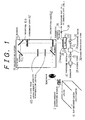
- FIG. 1 is a conceptual, constitutional explanatory view showing an example of equipment components for executing a process for the formation a cap layer of a semiconductors according to the present invention.
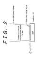
- the equipment shown in FIG. 1 is laser irradiating equipment wherein an ammonia gas being a gas containing nitrogen atom is used as a component element, and pulse laser beam is irradiated on a semiconductor (an InP substrate in the present embodiment) in ammonia gas atmosphere under normal pressure (760 Torr) to carry out a heating treatment (hereinafter referred optionally to as "laser irradiation treatment") is provided with a KrF excimer laser oscillator 10 generating pulse laser beam; a laser energy adjusting mirror 12 for adjusting laser energy of pulse laser beam output from the KrF excimer laser oscillator 10; a mirror 14 for inputting the pulse laser beam output from the laser energy adjusting mirror 12 to a projection system 16 which will be mentioned hereunder; a projection system 16 for homogenizing a laser energy density of the pulse laser beam input through the mirror 14 as well as for setting an irradiation region thereof; and a vacuum chamber 24 having a synthetic quartz window 18 disposed for adapting in such that the pulse laser
- the respective components are located in such that pulse laser beam output from the projection system 16 through the synthetic quartz window 18 is irradiated on the sample 22 placed on the sample table 20 inside the vacuum chamber 24.
- a well-known vacuum system composed of a turbo molecular pump 26, a rotary pump 28, valve 30, a valve 32, and a pressure gauge 34 and the like is connected to the vacuum chamber 24, whereby the interior of the vacuum chamber 24 can be adapted to be in a vacuum state as occasion demands.
- N 2 nitrogen gas
- NH 3 ammonia gas
- the above described projection system 16 includes a mirror 16a for deviating an optical path of pulse laser beam input through the mirror 14; fly's eye type laser energy density homogenizing devices 16b, 16b each homogenizing a laser energy density of the pulse laser beam the optical path of which was deviated by the mirror 16a; a mirror 16c and a mirror 16d each for deviating an optical path of the pulse laser beam output from the fly's eye type laser energy density homogenizing device 16b; an aperture 16e provided with an opening for setting an irradiation region of pulse laser beam (2.2 mm x 2.2 mm (in case of laser irradiation treatment) or 4 mm x 4 mm (in case of measurement or the like after the laser irradiation treatment) in the present embodiment) as a result of passing the pulse laser beam, the optical path of which was deviated by the mirror 16d, through the opening; a condenser lens 16f for condensing the pulse laser beam with which has been set an irradiation region as
- Reference numeral 40 designates a pressure gauge for measuring a pressure in the vacuum chamber 24.
- the InP (100) substrate being the sample 22 was rested on the sample table 20 in the vacuum chamber 24, and then N 2 purge was made by introducing nitrogen gas into the vacuum chamber 24 through the pipeline 36.
- ammonia gas was introduced into the vacuum chamber 24 through the pipeline 36 to fill up the vacuum chamber under a pressure of 760 Torr, and pulse laser beam output from the KrF excimer laser oscillator 10 was irradiated on a surface of the InP (100) substrate to heat the surface of the InP (100) substrate.
- component elements in the vicinity of a surface region of the InP (100) substrate being the sample 22 to which pulse laser beam has been irradiated combine with nitrogen atom, whereby the vicinity of the surface region to which has been irradiated pulse laser beam is nitrided, so that a thin film of InN x and PN x (InN x -PN x thin film) is formed as a nitride compound being the one passivated chemically on the surface of the InP (100) substrate.
- the nitride compound of InN x -PN x thin film formed on the surface of the InP (100) substrate can prevent oxidation on the surface of the InP (100) substrate in the atmosphere, so that the InN x -PN x thin film functions as a cap layer for the surface of the InP (100) substrate.
- FIG. 3 is a graphical representation indicating changes in XPS spectra of nitrogen (Nls) in an InP (100) substrate after nitriding a surface of the InP (100) substrate as a result of irradiating pulse laser beam with respect to the surface of the InP (100) substrate by changing irradiation pulse number
- FIG. 4 is a graphical representation indicated by irradiation pulse number dependency obtained by integrating the respective spectra shown in FIG. 3.
- an integrated value corresponds to the total area of the peaks, it is in a relationship in response to an amount of nitrogen (N) incorporated into the InP (100) substrate.
- an amount of nitrogen (N) incorporated into an InP (100) substrate increases with increase in irradiation pulse number of pulse laser beam.
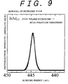
- FIG. 5 is a graphical representation indicating changes of XPS spectra of indium (In3d 5/2 ) in an InP substrate after nitriding a surface of the InP substrate by changing irradiation pulse number to irradiate pulse laser beam with respect to the surface of the InP substrate.
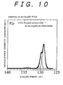
- FIG. 6 is a graphical representation indicating changes of XPS spectra of phosphorus (P2p) in an InP substrate after nitriding a surface of the InP substrate by changing irradiation pulse number to irradiate pulse laser beam with respect to the surface of the InP substrate.
- InN and P 3 N 5 each having a nearly stoichiometrical composition are formed on a surface of the InP (100) substrate.
- a thickness t of the InN x -PN x thin film formed on the surface of an InP (100) substrate became about 10 nm or less in the case where 2500 pulses of pulse laser beam were irradiated. Functions of a cap layer can be achieved sufficiently so far as the thin film has a thickness of such degree as described above.
- FIG. 7 is a graphical representation indicating changes in XPS spectra of indium (In3d 5/2 ) with respect to an InP substrate which had been maintained for 22 days in the atmosphere after a surface thereof was nitrided; and
- FIG. 8 is a graphical representation indicating similar changes in XPS spectra of phosphorus (P2p) in the same condition as that in the description of FIG. 7.
- the InN x -PN x thin film has a function for suppressing oxide formation, so that the InN x -PN x thin film functions sufficiently as a cap layer.
- nitrogen (N) is essentially an element of the group V, it forms a mixed crystal as a component element in III-V compound semiconductors (for example, GaAs 1-x N x is formed in the case where N is introduced into GaAs, while GaP 1-x N x is formed in the case where N is introduced into GaP).
- a degree of solid solution of nitrogen (N) in III-V compound semiconductors is as low as several percent as described above, so that such amount of nitrogen (N) does not combine with all the component elements on the surface of an InP substrate, and thus, the InP substrate cannot avoid oxidation thereof in the atmosphere.
- InP is a material required for formation of a high performance device as described above, but it is difficult to realize surface passivation as compared with that of GaAs and the like.
- nitrogen (N) has been introduced into a target InP (100) substrate as described above to nitride a surface of the InP (100) substrate thereby to realize surface passivation of the InP (100) substrate.
- a cap layer for III-V compound semiconductors can be formed by employing nitrogen being an element belonging to the same group as component elements for the III-V compound semiconductors without employing sulfur capable of being applied for a donor (electron feed source) in the III-V compound semiconductors, so that it becomes possible that a surface is protected with low contamination, and such surface is passivated, whereby oxidation with respect to the surface can be suppressed.
- the present invention Since the present invention has been constituted as described above, it exhibits an excellent advantage for providing a process for the formation of a cap layer for semiconductors with a low degree of contamination wherein the cap layer is easily formed on the surface of a semiconductor, and binding force thereof with the surface of the semiconductor is strong and stabilized, besides only the cap layer is selectively removed easily.
Landscapes
- Formation Of Insulating Films (AREA)
- Junction Field-Effect Transistors (AREA)
- Semiconductor Lasers (AREA)
Abstract
Description
Claims (9)
- A process for the formation of a cap layer for semiconductors comprising:introducing nitrogen atom into a surface of a semiconductor;combining a component element of said semiconductor in the vicinity of the surface of said semiconductor into which said nitrogen atom has been introduced with said nitrogen atom to form a nitride compound being a compound of said component element of the semiconductor and said nitrogen atom on the surface of said semiconductor; andutilizing said nitride compound as a cap layer for the surface of said semiconductor.
- A process for the formation of a cap layer for semiconductors comprising:disposing a semiconductor in a gas containing nitrogen atom as a component element;heat-treating a surface of said semiconductor thereby to introduce the nitrogen atom contained in said gas into a surface of a semiconductor;combining a component element of said semiconductor in the vicinity of the surface of said semiconductor into which the nitrogen atom contained in said gas has been introduced with the nitrogen atom contained in said gas to form a nitride compound being a compound of said component element of the semiconductor and the nitrogen atom contained in said gas on the surface of said semiconductor; andutilizing said nitride compound as a cap layer for the surface of said semiconductor.
- A process for the formation of a cap layer for semiconductors as claimed in claim 2 wherein said heat treatment for the surface of the semiconductor is such an instantaneous heat treatment that the surface of said semiconductor is instantaneously heated, and then cooled instantaneously, whereby a temperature in said surface of the semiconductor is maintained at a low temperature.
- A process for the formation of a cap layer for semiconductors as claimed in claim 3 wherein said instantaneous heat treatment is executed by irradiating pulse laser beam having a predetermined frequency and a predetermined fluence onto the surface of said semiconductor with a predetermined pulse number.
- A process for the formation of a cap layer for semiconductors as claimed in claim 1 wherein said semiconductor is a III-V compound semiconductor.
- A process for the formation of a cap layer for semiconductors as claimed in claim 2 wherein said semiconductor is a III-V compound semiconductor.
- A process for the formation of a cap layer for semiconductors as claimed in claim 3 wherein said semiconductor is a III-V compound semiconductor.
- A process for the formation of a cap layer for semiconductors as claimed in claim 4 wherein said semiconductor is a III-V compound semiconductor.
- A process for the formation of a cap layer for semiconductors comprising:disposing, as a semiconductor, InP being a III-V compound semiconductor in ammonia gas being a gas containing nitrogen atom as a component element;heat-treating a surface of said InP in such a manner that pulse laser beam having a predetermined frequency and a predetermined fluence is irradiated onto the surface of said InP with a predetermined pulse number while maintaining a temperature in the surface of said InP at a low temperature thereby to introduce the nitrogen atom contained in said ammonia gas into the surface of said InP;combining In and P being component elements of said InP in the vicinity of the surface of said InP into which the nitrogen atom contained in said ammonia gas has been introduced with the nitrogen atom contained in said ammonia gas to form a thin film of InNx and PNx being a compound of In and P being the component elements of said InP and the nitrogen atom contained in said ammonia gas on the surface of said InP; andutilizing said thin film of the InNx and PNx as a cap layer for the surface of said InP.
Applications Claiming Priority (2)
| Application Number | Priority Date | Filing Date | Title |
|---|---|---|---|
| JP2000018612 | 2000-01-27 | ||
| JP2000018612A JP2001210640A (en) | 2000-01-27 | 2000-01-27 | Method of forming semiconductor protective film |
Publications (2)
| Publication Number | Publication Date |
|---|---|
| EP1120821A2 true EP1120821A2 (en) | 2001-08-01 |
| EP1120821A3 EP1120821A3 (en) | 2004-07-28 |
Family
ID=18545440
Family Applications (1)
| Application Number | Title | Priority Date | Filing Date |
|---|---|---|---|
| EP01300686A Withdrawn EP1120821A3 (en) | 2000-01-27 | 2001-01-25 | Process for formation of cap layer for semiconductor |
Country Status (4)
| Country | Link |
|---|---|
| US (1) | US6432848B2 (en) |
| EP (1) | EP1120821A3 (en) |
| JP (1) | JP2001210640A (en) |
| CA (1) | CA2332739A1 (en) |
Families Citing this family (6)
| Publication number | Priority date | Publication date | Assignee | Title |
|---|---|---|---|---|
| US20030219917A1 (en) * | 1998-12-21 | 2003-11-27 | Johnson Ralph H. | System and method using migration enhanced epitaxy for flattening active layers and the mechanical stabilization of quantum wells associated with vertical cavity surface emitting lasers |
| US20050211950A1 (en) * | 2004-03-24 | 2005-09-29 | Cabot Microelectronics Corporation | Chemical-mechanical polishing composition and method for using the same |
| CA2581614A1 (en) | 2004-10-01 | 2006-04-13 | Finisar Corporation | Vertical cavity surface emitting laser having multiple top-side contacts |
| US7860137B2 (en) | 2004-10-01 | 2010-12-28 | Finisar Corporation | Vertical cavity surface emitting laser with undoped top mirror |
| US8329541B2 (en) * | 2007-06-15 | 2012-12-11 | Taiwan Semiconductor Manufacturing Company, Ltd. | InP-based transistor fabrication |
| US9905459B1 (en) * | 2016-09-01 | 2018-02-27 | International Business Machines Corporation | Neutral atom beam nitridation for copper interconnect |
Family Cites Families (3)
| Publication number | Priority date | Publication date | Assignee | Title |
|---|---|---|---|---|
| JPS56162841A (en) * | 1980-05-20 | 1981-12-15 | Nippon Telegr & Teleph Corp <Ntt> | Forming method for insulating film of compound semiconductor |
| US4735921A (en) * | 1987-05-29 | 1988-04-05 | Patrick Soukiassian | Nitridation of silicon and other semiconductors using alkali metal catalysts |
| GB2332563A (en) * | 1997-12-18 | 1999-06-23 | Sharp Kk | Growth of group III nitride or group III-V nitride layers |
-
2000
- 2000-01-27 JP JP2000018612A patent/JP2001210640A/en active Pending
-
2001
- 2001-01-25 EP EP01300686A patent/EP1120821A3/en not_active Withdrawn
- 2001-01-26 US US09/769,386 patent/US6432848B2/en not_active Expired - Fee Related
- 2001-01-26 CA CA002332739A patent/CA2332739A1/en not_active Abandoned
Also Published As
| Publication number | Publication date |
|---|---|
| CA2332739A1 (en) | 2001-07-27 |
| US20010021539A1 (en) | 2001-09-13 |
| US6432848B2 (en) | 2002-08-13 |
| JP2001210640A (en) | 2001-08-03 |
| EP1120821A3 (en) | 2004-07-28 |
Similar Documents
| Publication | Publication Date | Title |
|---|---|---|
| US5616947A (en) | Semiconductor device having an MIS structure | |
| EP2050126B1 (en) | GROWTH OF MONOCRYSTALLINE GeN ON A SUBSTRATE | |
| US10541315B2 (en) | INP-based transistor fabrication | |
| EP0964453A2 (en) | Article comprising an oxide layer on a GaAs-Based semiconductor body, and method of making the article | |
| US6989556B2 (en) | Metal oxide compound semiconductor integrated transistor devices with a gate insulator structure | |
| Green et al. | Do we need a new methodology for GaAs passivation? | |
| CN102498542A (en) | Semiconductor substrate, field effect transistor, integrated circuit, and method for producing semiconductor substrate | |
| US7187045B2 (en) | Junction field effect metal oxide compound semiconductor integrated transistor devices | |
| US6432848B2 (en) | Process for formation of cap layer for semiconductor | |
| US6670651B1 (en) | Metal sulfide-oxide semiconductor transistor devices | |
| Mehdi et al. | Investigation of N2 plasma GaAs surface passivation efficiency against air exposure: towards an enhanced diode | |
| US10541130B2 (en) | Indium gallium arsenide surface passivation by sulfur vapor treatment | |
| US5747838A (en) | Ultra-low phase noise GaAs MOSFETs | |
| US6936900B1 (en) | Integrated transistor devices | |
| Nishizawa et al. | Optimization of low temperature surface treatment of GaAs crystal | |
| Oyama et al. | Selective MLE growth of GaAs and surface treatment for ideal static induction transistor (ISIT) application | |
| Ito et al. | Thermal nitridation of silicon in advanced LSI processing | |
| Zhang et al. | Cl2/Ar High‐Density‐Plasma Damage in GaN Schottky Diodes | |
| Rocha | Optimization of dielectric/GaN interface for MIS gate power devices | |
| Malhotra et al. | Passivation of GaAs and InP | |
| Chanthaphan | Study on Bias-temperature Instability in 4H-SiC Metal-oxide-semiconductor Devices | |
| L'vova et al. | Liquid-phase epitaxial growth of GaSb-related compounds on sulphide treated (100) GaSb substrates | |
| Takahashi et al. | Oxide-free InP MIS structures having an ultra-narrow silicon surface quantum well | |
| Arokiaraj et al. | Surface and Bulk Passivation effect of GaAs grown on Si Substrates by SeS2Treatment | |
| Kapila | Passivation of III-V semiconductor surfaces and related devices |
Legal Events
| Date | Code | Title | Description |
|---|---|---|---|
| PUAI | Public reference made under article 153(3) epc to a published international application that has entered the european phase |
Free format text: ORIGINAL CODE: 0009012 |
|
| AK | Designated contracting states |
Kind code of ref document: A2 Designated state(s): AT BE CH CY DE DK ES FI FR GB GR IE IT LI LU MC NL PT SE TR |
|
| AX | Request for extension of the european patent |
Free format text: AL;LT;LV;MK;RO;SI |
|
| PUAL | Search report despatched |
Free format text: ORIGINAL CODE: 0009013 |
|
| AK | Designated contracting states |
Kind code of ref document: A3 Designated state(s): AT BE CH CY DE DK ES FI FR GB GR IE IT LI LU MC NL PT SE TR |
|
| AX | Request for extension of the european patent |
Extension state: AL LT LV MK RO SI |
|
| AKX | Designation fees paid | ||
| REG | Reference to a national code |
Ref country code: DE Ref legal event code: 8566 |
|
| STAA | Information on the status of an ep patent application or granted ep patent |
Free format text: STATUS: THE APPLICATION IS DEEMED TO BE WITHDRAWN |
|
| 18D | Application deemed to be withdrawn |
Effective date: 20050129 |