BACKGROUND OF THE INVENTION
Field of the Invention
This invention relates to a transparent electrode, a patterning method for the
same, and a manufacturing method for a semiconductor element of the same
formed on a transparent substrate used in an integrated type photovoltaic
device, a liquid crystal display device, and an organic EL device or the like.
Description of the prior art
A photovoltaic device comprising an amorphous semiconductor of amorphous
silicon, amorphous silicon carbide, amorphous silicon germanium or the like
has been developed as a solar cell device because it is manufactured at low
cost and easily increases in size.
Explanation of a general amorphous photovoltaic device is made by referring
to Fig. 35. A photovoltaic element 100 of an amorphous semiconductor is
formed by laminating a transparent electrode 102, a photovoltaic conversion
layer 103 of a lamination of p-, i-, and n-type amorphous semiconductor
layers 103p, 103i, 103n, and a rear surface metal electrode 104 in this order
on a glass substrate 101.
Tin oxide (SnO2) and ITO (Indium Tin Oxide) are used conventionally as
transparent conductive material for forming the transparent electrode 102. In
recent years, zinc oxide (ZnO) has been examined in order to reduce
manufacturing cost and provide a photovoltaic element having high
photovoltaic characteristics.
A photovoltaic element using ZnO is manufactured by the following processes.
For example, a transparent electrode 102 of ZnO is formed on a glass
substrate 101 by sputtering, and a photovoltaic conversion layer 103 formed
of a lamination of a p-type layer 103p of approximately 150Å of p-type
amorphous silicon carbide, an i-type layer 103i of approximately 4000Å of
i-type amorphous silicon, and an n-type layer 103n of approximately 200Å of
n-type amorphous silicon is formed by plasma CVD. Then, a rear surface
metal electrode 104 of silver (Ag) is sequentially laminated by sputtering to
manufacture the photovoltaic element 100.
Photovoltaic elements including transparent electrodes 102 of ZnO of various
thickness are manufactured and the photovoltaic conversion efficiency of
them are measured. The results are shown in Fig. 36. As shown in a
characteristic diagram of Fig. 36, high photovoltaic conversion efficiency over
10.5% is obtained when a thickness of the transparent electrode 102 is
approximately 2100-5000Å.
The photovoltaic element using the transparent electrode of ZnO can provide
high photovoltaic conversion efficiency.
The photovoltaic device comprising the amorphous semiconductor has an
integrated structure so as to take out a high voltage from a single substrate.
In order to form the integrated structure, it is necessary to separate the
transparent electrode film, the amorphous semiconductor layer, and the
metal electrode film on the glass substrate. A laser patterning method is used
for the separation.
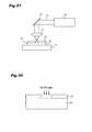
A structure of a laser patterning device is explained by referring to Fig. 37. A
laser 11 emitted from an Nd:YAG laser oscillating device 10 changes its
direction at a reflection mirror 12, is condensed by a condensing lens 13, and
irradiates a region to be processed of an object to be processed 20 mounted
on a moving table 14 of an XYZ stage. A pattern is controlled by moving the
moving table 14 with the object to be processed 20 mounted thereon.
In patterning a transparent electrode by using this device, the transparent
substrate 21 with the transparent electrode film 22 formed on the whole
surface thereof as the object to be processed is mounted on the moving table
14. The moving table 14 is controlled to move in XYZ directions so that the
region to be processed of the transparent electrode 22 is eliminated by laser
as shown in Fig. 38.
In the meantime, when the ZnO film formed by sputtering as the transparent
electrode on the transparent substrate (a glass substrate) 21 is
laser-patterned by an Nd:YAG laser (a wavelength of 1064nm, power 10W,
and a beam diameter 50 µm), phenomena particular to the ZnO film, which is
not observed when using material such as SnO2 and ITO as the transparent
electrode, are found. That is, (1) volume expansion of a laser irradiated end
part, (2) a crack of a laser irradiated end part, (3) peeling of the ZnO film from
the glass substrate, (4) diffusion of a ZnO forming element into the glass
substrate, or the like.
These phenomena seem to complicatedly relate to a crystalline structure,
heat conductivity, a surface tension in melting or the like of ZnO material.
These phenomena may result in short-circuit between electrodes of the
photovoltaic device, degraded reliability of the photovoltaic device, separation
failure of the ZnO film (insulation failure between adjacent photovoltaic
elements), and these problems obstruct commercialization of the ZnO
material. The photovoltaic element using the transparent electrode of the ZnO
film can not provide sufficient characteristics as an integrated type
photovoltaic device while it can provide high photovoltaic conversion
efficiency.
It is generally known that the ZnO material has moisture absorption property.
Therefore, when the ZnO film is retained in an atmosphere over a day,
moisture in the atmosphere penetrates from a surface of the ZnO film and
solid state properties change, resulting in significant failure of laser
patterning.
Fig. 39 is results of temperature distribution simulation in laser patterning;
an Nd:YAG laser (wavelength 1064nm, power 10W, a beam diameter 50 µm)
is irradiated to an aluminum dope ZnO film(7500Å in thickness) formed on a
glass substrate by sputtering. In this simulation, it is assumed that laser
energy injected to the ZnO film (laser energy excluding reflection and
transmission loss) is converted into heat energy.
The laser-irradiated ZnO film is required to be evaporated (scattered) with the
temperature reaching over the melting point and be completely eliminated so
as to obtain complete electrical insulation by laser patterning. The ZnO film is
required to melt to an interface of the glass and the ZnO film completely. In
this case, a temperature of the ZnO film on a surface side reaches over the
melting point and is in a high temperature state.
The excessive energy not only is converted into kinetic energy of a ZnO
molecule but also moves to a periphery of a laser irradiated part by heat
conduction, resulting in following heat damages; (1) volume expansion of the
laser irradiated end part, (2) a crack of the laser irradiated end part, (3)
peeling of the ZnO film from the glass substrate, (4) diffusion of the ZnO
forming element in the glass substrate.
These problems may cause short-circuit passing through a semiconductor
layer later formed, or a crack generated in the ZnO film in other processes
may cause loss of a part of the film and degradation of reliability. In addition,
diffusion of component elements of the ZnO film to the glass substrate causes
separation failure (electrical insulation failure).
The above simulation is made in assumption that all laser energy is converted
into heat energy. However, in actually dividing the ZnO film into a plurality of
electrodes by laser patterning, absorption of a laser is insufficient when the
ZnO film is thin, resulting in incomplete electrical separation.
A ZnO film having various thickness is formed on a glass substrate, and is
divided into two electrodes by laser patterning. Then resistance between the
two electrodes is measured. Fig. 40 is a characteristic view showing relations
between a thickness of the ZnO film and yields of non-defective item having
resistance between the electrodes not less than 10MΩ.
A separation width of the two electrodes is approximately 100 µm as in the
case of using for a photovoltaic device. It is found that high yields of over 90%
can be obtained when a thickness of the ZnO film is larger than 5000Å but
as a thickness becomes small, the yield declines. When the thickness is
smaller than 4500Å, yields is as low as under 40%.
The measurements show whether the film is completely separated depending
on resistance between the electrodes. When the thickness is large, as shown
in Fig. 39, a temperature on a surface of the ZnO film is far higher than the
melting point and deficiency particular to the ZnO film may occur. Therefore,
when the ZnO film with merely a large thickness is used as a transparent
electrode of the photovoltaic device, degradation of characteristics and
reliability may occur.
SUMMARY OF THE INVENTION
This invention was made to use a transparent electrode film for a photovoltaic
device of a ZnO film (gallium dope ZnO and aluminum dope ZnO) film which
is manufactured at low cost as compared with conventionally used SnO2, ITO
or the like. In addition, this invention was made to provide a transparent
electrode and a manufacturing method thereof capable of preventing
phenomena (heat damages, insulation failure or the like) particular to the
ZnO film appearing in a laser patterning process for forming the integrated
type photovoltaic device.
A transparent electrode according to this invention is formed by patterning a
transparent electrode film formed on a transparent substrate with a laser,
and comprises a transparent electrode film having a lower melting point than
that of a ZnO film and the ZnO film laminated in this order on the
transparent substrate.
As described above, the transparent electrode having a lower melting point is
provided on a side apart from the surface to be irradiated with a laser, thus
injection of excessive laser energy higher than the melting point of the
material becomes unnecessary, resulting in suppression of heat damage
(volume expansion, a crack) on the end part to be irradiated with a laser.
An ITO film may be used as a transparent electrode film having a lower
melting point than that of the ZnO film.
Because the melting point of the ITO film is lower than that of the ZnO film,
excessive laser energy higher than the melting point of the material becomes
unnecessary, resulting in suppression of heat damage of a laser irradiated
end part.
The ITO film may be 100-1000Å, and the ZnO film may be 2500-5000Å.
With this structure, good conversion efficiency and a good release voltage are
obtained from a photovoltaic device using this transparent electrode.
The transparent electrode film having the lower melting point than that of the
ZnO film is a metal thin film.
The metal thin film may be formed of silver and is 50-300Å.
With this structure, good conversion efficiency and a good release voltage are
obtained from a photovoltaic device using this transparent electrode.
The metal thin film is formed of aluminum and is 50-100Å.
With this structure, good conversion efficiency and a good release voltage are
obtained from a photovoltaic device using this transparent electrode.
A moisture proof layer containing nitrogen may be formed on a surface of the
ZnO film.
The moisture proof layer prevents moisture from penetrating from a surface
of the ZnO film so that workability of laser-patterning is not degraded. In
addition, long-term reliability of the ZnO film is improved.
In a patterning method for a transparent electrode according to this invention,
a transparent electrode film having a lower melting point than that of a ZnO
film is formed on a transparent substrate, a ZnO film is formed on the
transparent electrode film, and regions to be irradiated of the transparent
electrode film and the ZnO film are eliminated and patterned by laser
irradiation.
As described above, the transparent electrode having a lower melting point is
provided on a side apart from the surface to be irradiated with a laser, thus
injection of excessive laser energy higher than the melting point of the
material becomes unnecessary, resulting in suppression of heat damage
(volume expansion, a crack) on the end part to be irradiated with a laser.
A moisture proof layer containing nitrogen is formed on a surface of the ZnO
film.
The moisture proof layer prevents moisture from penetrating from a surface
of the ZnO film so that workability of laser-patterning is not degraded. In
addition, long-term reliability of the ZnO film is improved.
An ITO film as the transparent electrode film having the lower melting point
than that of the ZnO film is formed by sputtering.
The transparent substrate is a glass substrate and a crystallized glass layer is
provided between the glass substrate and the ITO film.
The crystallized glass layer prevents the ZnO component element from
diffusing to the glass substrate in laser-patterning.
The ITO film may be 100-1000Å, and the ZnO film may be 2500-5000Å.
With this structure, good conversion efficiency and a good release voltage are
obtained from a photovoltaic device using this transparent electrode.
The transparent electrode film having the lower melting point than that of the
ZnO film may be a metal thin film.
The metal thin film is formed of silver and is 50-300Å.
With this structure, good conversion efficiency and a good release voltage are
obtained from a photovoltaic device using this transparent electrode.
The metal thin film is formed of aluminum and is 50-100Å.
With this structure, good conversion efficiency and a good release voltage are
obtained from a photovoltaic device using this transparent electrode.
A manufacturing method for a semiconductor element according to this
invention comprises a process for forming a transparent electrode film having
a lower melting point than that of a ZnO film on a transparent substrate and
forming a ZnO film on the transparent electrode film, a process for forming a
plurality of transparent electrodes on the transparent substrate by irradiating
laser on the ZnO film and eliminating and patterning regions to be irradiated
of the transparent electrode film and the ZnO film, a process for forming a
photovoltaic conversion layer of an amorphous semiconductor on the
transparent substrate with the plurality of divided transparent electrodes
included, and a process for forming a highly reflective conductive film on the
photovoltaic conversion layer.
The manufacturing method for the semiconductor element according to this
invention further comprises a process for separating the previously formed
photovoltaic conversion layer into a plurality of photovoltaic conversion layers
by laser irradiation, and a process for dividing into a plurality of electrodes by
laser irradiation to the previously formed highly reflective conductive film.
Through these processes, good conversion efficiency and a good release
voltage are obtained from a photovoltaic device using this transparent
electrode.
BRIEF DESCRIPTION OF THE DRAWINGS
Fig. 1 is a cross sectional view illustrating a transparent electrode according
to this invention;
Fig. 2 is a partially enlarged view illustrating an optical system of a
laser-irradiated part according to this invention;
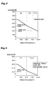
Fig. 3 shows a temperature distribution simulation of laser irradiation power
in patterning the transparent electrode according to this invention with an
Nd:YaG laser of a wavelength 1064nm, power 8W, and a beam diameter 50
µm;
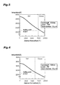
Fig. 4 shows a temperature distribution simulation of laser irradiation power
in patterning the transparent electrode with an Nd:YaG laser;
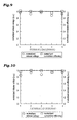
Fig. 5 shows a temperature distribution simulation of laser irradiation power
in patterning the transparent electrode with an Nd:YaG laser;
Fig. 6 shows a temperature distribution simulation of laser irradiation power
in patterning the transparent electrode with an Nd:YaG laser;
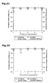
Fig. 7 is a characteristic view in measuring a normalized release voltage and
normalized conversion efficiency when an ITO film is 50Å and a ZnO film is
2500Å;
Fig. 8 is a characteristic view in measuring a normalized release voltage and
normalized conversion efficiency when the ITO film is 100Å and the ZnO film
is 2500Å;
Fig. 9 is a characteristic view in measuring a normalized release voltage and
normalized conversion efficiency when the ITO film is 500Å and the ZnO film
is 2500Å;
Fig. 10 is a characteristic view in measuring a normalized release voltage and
normalized conversion efficiency when the ITO film is 1000Å and the ZnO
film is 2500Å;
Fig. 11 is a characteristic view in measuring a normalized release voltage and
normalized conversion efficiency when the ITO film is 50Å and the ZnO film
is 3000Å;
Fig. 12 is a characteristic view in measuring a normalized release voltage and
normalized conversion efficiency when the ITO film is 100Å and the ZnO film
is 3000Å;
Fig. 13 is a characteristic view in measuring a normalized release voltage and
normalized conversion efficiency when the ITO film is 500Å and the ZnO film
is 3000Å;
Fig. 14 is a characteristic view in measuring a normalized release voltage and
normalized conversion efficiency when the ITO film is 1000Å and the ZnO
film is 3000Å;
Fig. 15 is a characteristic view in measuring a normalized release voltage and
normalized conversion efficiency when the ITO film is 50Å and the ZnO film
is 4000Å;
Fig. 16 is a characteristic view in measuring a normalized release voltage and
normalized conversion efficiency when the ITO film is 100Å and the ZnO film
is 4000Å;
Fig. 17 is a characteristic view in measuring a normalized release voltage and
normalized conversion efficiency when the ITO film is 500Å and the ZnO film
is 4000Å;
Fig. 18 is a characteristic view in measuring a normalized release voltage and
normalized conversion efficiency when the ITO film is 1000Å and the ZnO
film is 4000Å;
Fig. 19 is a characteristic view in measuring a normalized release voltage and
normalized conversion efficiency when the ITO film is 50Å and the ZnO film
is 5000Å;
Fig. 20 is a characteristic view showing a normalized release voltage and
normalized conversion efficiency when the ITO film is 100Å and the ZnO film
is 5000Å;
Fig. 21 is a characteristic view in measuring a normalized release voltage and
normalized conversion efficiency when the ITO film is 500Å and the ZnO film
is 5000Å;
Fig. 22 is a characteristic view in measuring a normalized release voltage and
normalized conversion efficiency when the ITO film is 1000Å and the ZnO
film is 5000Å;
Fig. 23 is a schematic view of a transparent electrode formed by sputtering;
Fig. 24 is a diagram indicating relations between exposure time and
normalized conversion efficiency at a certain atmospheric nitrogen
temperature in exposure;
Fig. 25 is a diagram indicating relations between exposure time and
normalized conversion efficiency at a certain atmospheric nitrogen
temperature in exposure;
Fig. 26 is a diagram indicating relations between exposure time and
normalized conversion efficiency at a certain atmospheric nitrogen
temperature in exposure;
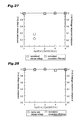
Fig. 27 is a characteristic view in measuring a normalized release voltage and
normalized conversion efficiency measured when the Ag film is 30Å and the
ZnO film is 5000Å;
Fig. 28 is a characteristic view in measuring a normalized release voltage and
normalized conversion efficiency measured when the Ag film is 50Å and the
ZnO film is 5000Å;
Fig. 29 is a characteristic view in measuring a normalized release voltage and
normalized conversion efficiency measured when the Ag film is 200Å and the
ZnO film is 5000Å;
Fig. 30 is a characteristic view in measuring a normalized release voltage and
normalized conversion efficiency measured when the Ag film is 300Å and the
ZnO film is 5000Å;
Fig. 31 is a characteristic view in measuring a normalized release voltage and
normalized conversion efficiency measured when the Al film is 30Å and the
ZnO film is 5000Å;
Fig. 32 is a characteristic view in measuring a normalized release voltage and
normalized conversion efficiency measured when the Al film is 100Å and the
ZnO film is 5000Å;
Fig. 33 is a characteristic view in measuring a normalized release voltage and
normalized conversion efficiency measured when the Al film is 30Å and the
ZnO film is 5000Å;
Fig. 34 is a characteristic view in measuring a normalized release voltage and
normalized conversion efficiency measured when the Al film is 150Å and the
ZnO film is 5000Å;
Fig. 35 is a cross sectional view illustrating a general amorphous photovoltaic
device;
Fig. 36 is a characteristic view indicating relations between a thickness of the
transparent electrode and photovoltaic conversion efficiency of the
photovoltaic element using the transparent electrode of the ZnO film;
Fig. 37 is a schematic view illustrating a structure of a laser patterning
device;
Fig. 38 is a cross sectional view illustrating a conventional transparent
electrode;
Fig. 39 is a temperature distribution simulation of laser irradiation power in
patterning the conventional transparent electrode with an Nd-YAG laser;
Fig. 40 is a characteristic view illustrating relation between a thickness and
yield when the ZnO film is used as the transparent electrode.
DESCRIPTION OF THE PREFERRED EMBODIMENTS
Embodiments of this invention are explained.
A ZnO film (gallium doped ZnO, and aluminum dope ZnO) of lower cost
material than SnO2 and ITO or the like used conventionally is used as a
transparent electrode film for a photovoltaic device according to this invention.
Heat damage on the ZnO film in a laser patterning process for forming an
integrated type photovoltaic device results from excessive injection of heat
energy higher than a melting point.
This invention provides a transparent electrode capable of laser-patterning
without injecting excessive heat energy higher than the melting point. As
shown in Fig, 1, the transparent electrode is provided with a crystallized glass
(Li2O-Al2O3-SiO2) layer 2 on a transparent glass substrate 1, and an ITO film
3 and a ZnO film 4 are laminated on the crystallized glass 2 by sputtering.
The ITO film has a lower melting point than that of the ZnO film. Because the
ITO film having the lower melting point is provided on a side far from a
surface to be irradiated with a laser, injection of excessive laser energy higher
than the melting point of material becomes unnecessary and heat damage on
the laser irradiated end part (volume expansion, a crack) is suppressed.
The crystallized glass (Li2O-Al2O3-SiO2) layer 2 formed on an interface of the
glass substrate 1 and the transparent electrode film prevents the ZnO
component element from diffusing to the glass substrate 1.
The laser used in this embodiment is an Nd-YAG laser (a wavelength 1064nm,
power 8W, a beam diameter 50 µm), and is shaped so as to have an
approximately uniform energy distribution to a region to be irradiated by
using an optical system shown in Fig. 2. An iris 16 (a round or rectangular
hole) having an aperture rate of approximately 25% to an incident diameter
from a center part of the laser is arranged on an optical path of a general
laser having normal energy distributions, the laser passing though the iris 16
is introduced to the condensing lens 13, the laser condensed by the
condensing lens 13 is irradiated to an object to be processed on the basis of
the conditions of the formula (1).
1/a + 1/b =1/f
With this structure, excessive heat given to a region except a region to be
eliminated (particularly, a peripheral region of the processed part) is reduced,
resulting in heat damage.
As the number of lamination of transparent electrode films is large, melting
point distributions close to actual temperature distributions can be achieved.
However, a transparent electrode film of a general photovoltaic device is
5000-10000Å in thickness and temperature gradient of more than 500K
occurs in the film when such the transparent electrode film is laser-patterned.
Fig. 39 shows results of a temperature distribution simulation in forming the
transparent electrode film of only the ZnO film and it is found that
temperature gradient of more than 500K occurs in the conventional film.
Figs. 4, 5, 6 show results of a temperature distribution simulation of laser
irradiation power optimized for each of three patterns of thickness of the
aluminum dope ZnO film. In this case, an optimizing condition is to control a
temperature of an interface of the glass and the ZnO film to be higher than a
melting point 2248K.
An Nd:YaG laser in Fig. 4 has a wavelength 1064nm, power 8W, and a beam
diameter 50 µm. Heat damage is not generated in Fig. 4, but is generated in
Figs. 5, 6. An Nd:YaG laser in Fig. 5 has a wavelength 1064nm, power 10W,
and a beam diameter 50 µm. An Nd:YaG laser in Fig. 6 has a wavelength
1064nm, power 9W, and a beam diameter 50 µm.
In Figs. 4-6, a difference between temperatures on surface parts, or a
temperature difference between the surface temperature and the melting
point, seems approximately 350K under the conditions for not generating
heat damage. It is preferred to form of at least two transparent electrode films
and have a thickness of each of the layers not larger than 5000Å so as to
suppress the temperature difference on the surface part within approximately
350K.
A crystallized glass layer 2 of 50Å is formed on a transparent glass substrate
1, an ITO film 3 of 2500Å and a ZnO film of 5000Å are formed in this order
on the crystallized glass layer 2. Fig. 3 shows a temperature distribution
simulation of laser irradiation power in patterning with an Nd:YAG laser (a
wavelength 1064nm, power 8W, a beam diameter 50 µm). In the transparent
electrode film of this invention formed as described above, a temperature
disparity on a surface part of the ZnO film 4, or a temperature difference
between the surface temperature and the melting point, is within
approximately 350K. At this time, the ITO film 3 on an interface between the
crystallized glass layer 2 and the ITO film 3 has a higher temperature than
the melting point and patterning is provided without heat damage.
When the transparent electrode of this embodiment is used as a transparent
electrode of an integrated photovoltaic device, sheet resistance and light
transmittivity of the transparent electrode should be considered
A thickness of the ZnO film is preferred to be not more than 5000Å in order
to provide patterning without heat damage as shown in Figs. 4-6. As shown
in Fig. 36, the photovoltaic element using the ZnO film as the transparent
electrode can obtain high photovoltaic efficiency when the thickness of the
ZnO film is approximately 2100-5000Å. A film formed by laminating the ZnO
film and other transparent electrode films is preferred to have a thickness of
approximately 2100-5000Å when the ZnO is used as main material for the
transparent electrode film. However, when the transparent electrode film is
formed of the ZnO element film, yields after divining the film by
laser-patterning declines significantly when the thickness is not larger than
4500Å as shown in Fig. 40.
A crystallized glass layer 2 of 50 Å is provided on a transparent glass
substrate 1, an ITO film 3 and a ZnO film 4 are formed in this order on the
crystallized glass substrate 2. Thickness of each of the films is varied and
patterned with an Nd:YAG laser (a wavelength 1064nm, power 8W, a beam
diameter 50 µm). An integrated type photovoltaic device is manufactured by
using this substrate. This integrated type photovoltaic device is formed as
follows. The substrate is laser-patterned to divide into a plurality of
transparent electrodes on the transparent glass substrate 1 and p-, I-, n-
types amorphous semiconductor layers are laminated in this order on an
approximately whole surface on the substrate 1 with the transparent
electrode included, and is divided into a plurality of photovoltaic conversion
layers by laser-patterning. Furthermore, a highly reflective conductive film is
formed on the approximately whole surface of the substrate with the plurality
of photovoltaic conversion layers and is divided into a plurality of rear surface
electrodes by laser-patterning.
A normalized release voltage and normalized conversion efficiency are
measured in comparison with a photovoltaic element of 1cm2 using the
transparent electrode film of the same lamination as a reference. "O"
indicates a normalized release voltage, "□" indicates normalized conversion
efficiency in the figures.
The ZnO film of samples in Figs. 7-10 is 2500Å and the ITO film has various
thickness.
Fig. 7 is a characteristic view in measuring a normalized release voltage and
normalized conversion efficiency when the ITO film is 50Å and the ZnO film
is 2500Å. The samples are produced by laminating the ITO film of 50Å and
the ZnO film of 2500Å on the glass substrate and dividing the lamination
film by laser patterning of the above conditions. The integrated type
photovoltaic device is manufactured by using these samples and a normalized
release voltage and normalized release efficiency are measured.
As shown in Fig. 7, the layers of these samples are not completely separated
and short-circuit is observed.
Fig. 8 is a characteristic view in measuring a normalized release voltage and
normalized conversion efficiency when the ITO film is 100Å and the ZnO film
is 2500Å. The samples are produced by the above described processes. When
the ITO film is 100Å and the ZnO film is 2500Å, characteristics equivalent
to those of a photovoltaic element of 1cm2 can be obtained in terms of a
normalized release voltage and normalized conversion efficiency. It is found
that an integrated type photovoltaic device of good characteristics is provided.
Fig. 9 is a characteristic view in measuring a normalized release voltage and
normalized conversion efficiency when the ITO film is 500Å and the ZnO film
is 2500Å. Fig. 10 is a characteristic view in measuring a normalized release
voltage and normalized conversion efficiency when the ITO film is 1000Å and
the ZnO film is 2500Å. The samples are produced by the above described
processes. As shown in Figs. 9, 10 good characteristics can be obtained as
the integrated type photovoltaic device although a little degradation of
characteristics is found as compared with Fig. 8.
The ZnO film of the samples in Figs. 11-14 is 3000Å and the ITO film has
various thickness.
Fig. 11 is a characteristic view in measuring a normalized release voltage and
normalized conversion efficiency when the ITO film is 50Å and the ZnO film
is 3000Å. The samples are produced by laminating the ITO film of 50Å and
the ZnO film of 3000Å in this order on the glass substrate and dividing the
lamination film by laser patterning of the above conditions. The integrated
type photovoltaic device is manufactured by using these samples and a
normalized release voltage and normalized release efficiency are measured.
As shown in Fig. 11, these samples are not completely separated and
short-circuit is found.
Figs. 12-14 are characteristic views in measuring a normalized release voltage
and normalized conversion efficiency respectively when the ITO film is 100Å
and the ZnO film is 3000Å, when the ITO film is 500Å and the ZnO film is
3000Å, and when the ITO film is 1000Å and the ZnO film is 3000Å. The
samples are produced through the above processes.
As shown in Figs. 12-14, when the ITO film is not less than 100Å in
thickness and the ZnO film is 3000Å, characteristics equivalent to those of a
photovoltaic element of 1cm2 can be obtained in terms of a normalized release
voltage and normalized conversion efficiency. It is found that an integrated
type photovoltaic device of good characteristics is provided.
The ZnO film of samples in Figs. 15-18 is 4000Å and the ITO film has
various thickness.
Fig. 15 is a characteristic view in measuring a normalized release voltage and
normalized conversion efficiency when the ITO film is 50Å and the ZnO film
is 4000Å. The samples are produced by laminating the ITO film of 50Å and
the ZnO film of 4000Å on the glass substrate and dividing the lamination
film by laser patterning of the above conditions. The integrated type
photovoltaic device is manufactured by using these samples and a normalized
release voltage and normalized release efficiency are measured.
As shown in Fig. 15, these samples are not completely separated and
short-circuit is observed.
Figs. 16-18 are characteristic views in measuring a normalized release voltage
and normalized conversion efficiency respectively when the ITO film is 100Å
and the ZnO film is 4000Å, when the ITO film is 500Å and the ZnO film is
4000Å, and when the ITO film is 1000Å and the ZnO film is 4000Å. The
samples are formed through the above processes.
As shown in Figs. 16-18, when the ITO film is not less than 100 Å in
thickness and the ZnO film is 4000Å, characteristics equivalent to those of a
photovoltaic element of 1cm2 can be obtained in terms of a normalized release
voltage and normalized conversion efficiency. It is found that an integrated
type photovoltaic device of good characteristics is provided.
The ZnO film of samples in Figs. 19-22 is 5000Å and the ITO film has
various thickness.
Fig. 19 is a characteristic view in measuring a normalized release voltage and
normalized conversion efficiency when the ITO film is 50Å and the ZnO film
is 5000Å. The samples are produced by laminating the ITO film of 50Å and
the ZnO film of 400Å on the glass substrate and dividing the lamination film
by laser patterning of the above conditions. The integrated type photovoltaic
device is manufactured by using these samples and a normalized release
voltage and normalized release efficiency are measured.
As shown in Fig. 19, these samples are not completely separated and
short-circuit is observed.
Figs. 20-22 are characteristic views in measuring a normalized release voltage
and normalized conversion efficiency respectively when the ITO film is 100Å
and the ZnO film is 5000Å, when the ITO film is 500Å and the ZnO film is
5000Å, and when the ITO film is 1000Å and the ZnO film is 5000Å. The
samples are produced through the above processes.
As shown in Figs. 20-22, when the ITO film is not less than 100 Å in
thickness and the ZnO film is 5000Å, characteristics equivalent to those of a
photovoltaic element of 1cm2 can be obtained in terms of a normalized release
voltage and normalized conversion efficiency. It is found that an integrated
type photovoltaic device of good characteristics is provided.
As shown in Figs. 7-22, advantages of this invention can be obtained when
the transparent electrode film having lamination of the ITO film and the ZnO
film has the thickness of ITO not less than 100Å. When the thickness of the
ITO is 1000Å, the integrated type photovoltaic device of good characteristics
is provided. Although the integrated type photovoltaic device of good
characteristic is obtained even when the ITO film is not less than 1000Å in
thickness, the thickness of the ITO is preferred to be 100-1000Å in terms of
manufacturing cost. In addition, when the thickness of the ZnO is 2500-5000
A, the integrated type photovoltaic device of good characteristics is provided.
It is generally known that ZnO material has moisture absorption property.
Therefore when the ZnO film is retained in the atmosphere for longer than
one day, moisture in the atmosphere penetrates from a surface of the ZnO
film and solid state properties change, resulting in significant laser patterning
failure. As shown in Fig. 23, the ITO film 3 is formed by sputtering on the
glass substrate 1 with the crystallized glass layer 2 formed thereon. After
forming the ZnO film 4 on the ITO film 3 by sputtering, it is exposed in a
nitrogen atmosphere, and a moisture proof layer containing nitrogen of a
nitrogen diffused layer or an absorbing layer is formed on the surface of the
ZnO film 4
A desired moisture proof layer formed on the surface of the ZnO film 4 is
exposed for different time depending on a substrate temperature. In Fig. 24,
an atmospheric temperature is a room temperature, and an effect of the
moisture proof layer is not obtained unless the film is exposed for longer than
12 hours. In Fig. 25, an atmospheric temperature is 100°C, and an effect of
the moisture proof layer is not obtained unless the film is exposed for longer
than 6 hours. In Fig. 26, an atmospheric temperature is 150°C, and an effect
of the moisture proof layer can not appear unless the film is exposed for
longer than one hours. In Figs. 24-26, normalized conversion efficiency is
indicated when the photovoltaic element formed on the transparent electrode
film is used as an SnO2 surface electrode as a reference.
The moisture proof layer prevents penetration of moisture from the surface of
the ZnO film and prevents degradation of workability of laser-patterning or
the like. In addition, long-term reliability of the ZnO film can be improved.
In the above embodiment, the ITO film having a lower melting point is
provided on a side far from a surface to be irradiated with a laser. The
transparent film having a lower melting point than that of the ZnO film and
having a thickness so as not to degrade the light transmittivity significantly,
can provid the same effect even when any other metal thin film is used. For
example, silver (Ag), aluminum (Al) or the like can be used. A minimum and
maximum value of thickness for not degrading light transmittivity and
obtaining the effect of this invention are obtained experimentally. Samples
are produced as in the case of the ITO film and experiments are conducted.
A crystallized glass layer 2 of 50Å is formed on a transparent glass substrate
1, an Ag or Al film 3 and a ZnO film 4 are formed on the crystallized glass
layer 2. A thickness of each of the layers are different in each of the different
samples. The substrates are patterned with an Nd:YAG laser and an
integrated type photovoltaic device is manufactured by using this substrate.
A normalized release voltage and a normalized conversion efficiency are
measured in comparison with a photovoltaic element of 1cm2 using the
transparent electrode film of ZnO element of 5000A. In these figures, "O"
indicates a normalized release voltage, "□" indicates a normalized conversion
efficiency.
The samples in Figs. 27-30 have the ZnO film of 5000Å and the Ag film of
different thickness.
Fig. 27 is a characteristic view in measuring a normalized release voltage and
normalized conversion efficiency when the Ag film is 30Å and the ZnO film is
5000Å. These samples are formed by laminating the Ag film of 30Å and the
ZnO film of 5000Å in this order on the glass substrate and the lamination is
divided by laser patterning under the above conditions. The integrated type
photovoltaic device is manufactured by using these samples and a normalized
release voltage and normalized release efficiency are measured.
As shown in Fig. 27, the normalized release voltage and normalized
conversion efficiency of the sample 2 are degraded significantly, and the
layers are not completely divided, resulting in occurrence of short-circuit.
Fig. 28 is a characteristic view in measuring a normalized release voltage and
normalized conversion efficiency when the Ag film is 50Å and the ZnO film is
5000Å. Samples are produced through the above processes. As shown in Fig.
28, when the Ag film is 50Å and the ZnO film is 5000Å, characteristics
equivalent to those of a photovoltaic element of 1cm2 can be obtained in
terms of a normalized release voltage and normalized conversion efficiency. It
is found that an integrated type photovoltaic device of good characteristics is
provided.
Fig. 29 is a characteristic view in measuring a normalized release voltage and
normalized conversion efficiency when the Ag film is 200Å and the ZnO film
is 5000Å. The samples are produced through the above processes. As shown
in Fig. 29, when the Ag film is not less than 200Å and the ZnO film is 5000
A, characteristics equivalent to a photovoltaic element of 1cm2 can be
obtained in terms of a normalized release voltage and normalized conversion
efficiency. It is found that an integrated type photovoltaic device of good
characteristics is provided.
Fig. 30 is a characteristic view in measuring a normalized release voltage and
normalized conversion efficiency when the Ag film is 300Å and the ZnO film
is 5000Å. Samples are produced through the above processes. As shown in
Fig. 30, characteristics of the normalized conversion efficiency are degraded a
little as compared with Figs. 28, 29. This seems because the thickness of the
Ag film increases and light transmittivity is degraded a little. However, an
integrated type photovoltaic device of good characteristics is provided in spite
of a little degradation of conversion efficiency.
It is found, from Figs. 27-30, that the Ag film of 50-300Å, preferably 50-200
Å is desirable in the transparent electrode film with the Ag film and the ZnO
film laminated.
Explanation is made on samples using an Al film as a metal thin film.
The samples in Figs. 31-34 have a ZnO film of 5000Å and an Al film of
different thickness.
Fig. 31 is a characteristic view in measuring a normalized release voltage and
normalized conversion efficiency when the Al film is 30Å and the ZnO film is
5000Å. These samples are formed by laminating the Al film of 30Å and the
ZnO film of 5000Å in this order on the glass substrate and the lamination is
divided by laser patterning under the above conditions. The integrated type
photovoltaic device is manufactured by using these samples and a normalized
release voltage and normalized release efficiency are measured.
As shown in Fig. 31, the normalized release voltage and normalized
conversion efficiency of the sample 1, 3 are degraded significantly, and the
layers are not sufficiently divided, resulting in occurrence of short-circuit.
Fig. 32 is a characteristic view in measuring a normalized release voltage and
normalized conversion efficiency when the Al film is 50Å and the ZnO film is
5000Å. Samples are produced through the above processes. As shown in Fig.
32, when the Al film is not less than 50Å and the ZnO film is 5000Å,
characteristics equivalent to those of a photovoltaic element of 1cm2 can be
obtained in terms of a normalized release voltage and normalized conversion
efficiency. It is found that an integrated type photovoltaic device of good
characteristics is provided.
Fig. 33 is a characteristic view in measuring a normalized release voltage and
normalized conversion efficiency when the Al film is 100Å and the ZnO film
is 5000Å. Samples are produced through the above processes. As shown in
Fig. 33, when the Al film is not less than 100Å and the ZnO film is 5000Å,
characteristics equivalent to those of a photovoltaic element of 1cm2 can be
obtained in terms of a normalized release voltage and normalized conversion
efficiency. It is found that an integrated type photovoltaic device of good
characteristics is provided.
Fig. 34 is a characteristic view in measuring a normalized release voltage and
normalized conversion efficiency when the Al film is 150Å and the ZnO film
is 5000Å. Samples are produced through the above processes. As shown in
Fig. 34, characteristics of the normalized conversion efficiency are degraded a
little as compared with in Figs. 32, 33. This seems because the thickness of
the Al film increases and light transmittivity is degraded a little.
It is preferred, as shown in Figs. 31-34, the thickness of the Al film is 50-100
Å in the transparent electrode film with the Al film and the ZnO film
laminated.
As described above, the transparent conductive thin film having a lower
melting point than that of the ZnO film is provided on a side apart from the
surface to be irradiated with a laser, thus injection of excessive laser energy
higher than the melting point of the material becomes unnecessary, resulting
in suppression of heat damage (volume expansion, a crack) on the end part to
be irradiated with a laser.
Although the present invention has been described and illustrated in detail, it
should be clearly understood that the description discloses examples of
different embodiments of the invention and is not intended to be limited to
the examples or illustrations provided. Any changes or modifications within
the spirit and scope of the present invention are intended to be included, the
invention being limited only by the terms of the appended claims.