EP1117199A1 - Régénération 3R d'un signal optique - Google Patents
Régénération 3R d'un signal optique Download PDFInfo
- Publication number
- EP1117199A1 EP1117199A1 EP01400062A EP01400062A EP1117199A1 EP 1117199 A1 EP1117199 A1 EP 1117199A1 EP 01400062 A EP01400062 A EP 01400062A EP 01400062 A EP01400062 A EP 01400062A EP 1117199 A1 EP1117199 A1 EP 1117199A1
- Authority
- EP
- European Patent Office
- Prior art keywords
- signal
- arms
- optical
- output
- regenerated
- Prior art date
- Legal status (The legal status is an assumption and is not a legal conclusion. Google has not performed a legal analysis and makes no representation as to the accuracy of the status listed.)
- Granted
Links
- 230000003287 optical effect Effects 0.000 title claims abstract description 29
- 238000011069 regeneration method Methods 0.000 title abstract description 7
- 230000008878 coupling Effects 0.000 claims abstract description 20
- 238000010168 coupling process Methods 0.000 claims abstract description 20
- 238000005859 coupling reaction Methods 0.000 claims abstract description 20
- 239000004065 semiconductor Substances 0.000 claims description 8
- 230000010363 phase shift Effects 0.000 claims description 6
- 230000001172 regenerating effect Effects 0.000 claims description 3
- 230000008929 regeneration Effects 0.000 abstract description 6
- 230000005540 biological transmission Effects 0.000 description 14
- 238000010586 diagram Methods 0.000 description 7
- 239000000835 fiber Substances 0.000 description 7
- 238000006243 chemical reaction Methods 0.000 description 6
- 239000013307 optical fiber Substances 0.000 description 4
- 230000003247 decreasing effect Effects 0.000 description 2
- 238000005259 measurement Methods 0.000 description 2
- 238000011084 recovery Methods 0.000 description 2
- 230000007423 decrease Effects 0.000 description 1
- 230000001419 dependent effect Effects 0.000 description 1
- 230000001066 destructive effect Effects 0.000 description 1
- 239000006185 dispersion Substances 0.000 description 1
- 235000021183 entrée Nutrition 0.000 description 1
- 238000002474 experimental method Methods 0.000 description 1
- 239000000284 extract Substances 0.000 description 1
- 238000001914 filtration Methods 0.000 description 1
- 238000003780 insertion Methods 0.000 description 1
- 230000037431 insertion Effects 0.000 description 1
- 230000014759 maintenance of location Effects 0.000 description 1
- 238000000034 method Methods 0.000 description 1
- 230000035945 sensitivity Effects 0.000 description 1
- 238000012163 sequencing technique Methods 0.000 description 1
- 230000008054 signal transmission Effects 0.000 description 1
- 230000003595 spectral effect Effects 0.000 description 1
- 230000003068 static effect Effects 0.000 description 1
- 238000012360 testing method Methods 0.000 description 1
Images



Classifications
-
- H—ELECTRICITY
- H04—ELECTRIC COMMUNICATION TECHNIQUE
- H04B—TRANSMISSION
- H04B10/00—Transmission systems employing electromagnetic waves other than radio-waves, e.g. infrared, visible or ultraviolet light, or employing corpuscular radiation, e.g. quantum communication
- H04B10/29—Repeaters
- H04B10/291—Repeaters in which processing or amplification is carried out without conversion of the main signal from optical form
- H04B10/299—Signal waveform processing, e.g. reshaping or retiming
-
- H—ELECTRICITY
- H04—ELECTRIC COMMUNICATION TECHNIQUE
- H04B—TRANSMISSION
- H04B10/00—Transmission systems employing electromagnetic waves other than radio-waves, e.g. infrared, visible or ultraviolet light, or employing corpuscular radiation, e.g. quantum communication
- H04B10/29—Repeaters
- H04B10/291—Repeaters in which processing or amplification is carried out without conversion of the main signal from optical form
- H04B10/2912—Repeaters in which processing or amplification is carried out without conversion of the main signal from optical form characterised by the medium used for amplification or processing
- H04B10/2914—Repeaters in which processing or amplification is carried out without conversion of the main signal from optical form characterised by the medium used for amplification or processing using lumped semiconductor optical amplifiers [SOA]
Definitions
- the invention lies in the field of optical signal regeneration circuits transmission of information. It is applicable to transmissions whose code is or is not with return to zero.
- interferometers whose arms include optical amplifiers with semiconductor for making decision windows. These interferometers that use a wave source continuous constituting the output carrier wave can be used in a configuration as opposed to phase (out of phase) or in phase.
- An interferometer whose arms include semiconductor optical amplifiers, can also be used in conjunction with a signal reconstructed clock. In this case, in particular when the converter is used as opposed to phase a good 3R regeneration is obtained.
- the capabilities of the transformed signal to resist deformations in line remain good provided that the clock pulses have a short duration by relative to the duration of each pulse constituting, together, the signal to be transmitted.
- interferometers whose arms have optical amplifiers with semiconductor, whether in phase or in opposition phase, does not provide good characteristics of decision window with a single interferometer. signal capabilities obtained at resist deformations online, are not enough good for direct use as a transmitter.
- Multi-storey architectures are therefore inevitable with the use of known techniques. Of more, these reconstitution solutions are not necessarily the most practical or the most efficient for the subsequent insertion of a sequencing by introducing a signal clock.
- wave resistance capacity pulse distortions may not be satisfactory. It is dependent on the flow of transmission and the device used to recover the clock. The transmission wavelength is also fixed by the clock source. In addition the signal clock signal-to-noise ratio low.
- the present invention is intended to remedy to these disadvantages.
- it aims to achieve device capable of regenerating 3R, a signal whose throughput can reach 40 gigabits per second and beyond. It also aims to reconcile a good window of decision, a weak deformation of the impulses in lines while reducing the number of components required.
- the regeneration circuit 1 includes a interferometric structure 10, for example of Mach-Zehnder, comprising a first arm 11 and a second arm 12.
- Input coupling means 13 couple the first arm 11 to guides, for example, optical fibers 15 and 16.
- the coupling means 13 couple the second arm 12 to the guide 16 on the one hand, and to a guide 17, for example, an optical fiber.
- Output coupling means 14 couple each of the arms 11, 12 to an outlet guide 18.
- Each of the arms 11, 12 has a semiconductor optical amplifier, 19, 20, respectively.
- the output guide 18 feeds a bandpass filter 21 whose output constitutes the output of device 1 according to the invention.
- the arm 16 is coupled to a generator of a continuous wave 34, and the arm 17 to a generator of a clock signal of the signal to be regenerated, preferably a recuperator of such a signal.
- each of the guides input 15-17 and output guide 18, can include optical amplifiers for example at semiconductor, 21-23 and 24 respectively, intended for adapt the level of the different signals.
- guide 16 receives the unmodulated continuous optical wave in source of the continuous wave generator 34.
- the guide 17 receives a clock signal from the clock signal generator 31, generating preferably a clock signal reformed from the signal to regenerate.
- Guides 15 and 16 feed the first arm 11.
- the medium 19 has an optical power of constant output as long as the input power is below a threshold then decreasing above this threshold.
- the curve representing the optical power input is shown in Figure 2.
- the power level of the continuous wave is adjusted by amplifier 22 to be at a level close to or higher than entry level Ps to from which the output power decreases.
- this continuous wave is after its passage in the middle 19 modulated in power by the power level received by the arm 11 from guide 15.
- the wave leaving the middle 19 of arm 11 is therefore modulated by the signal present on arm 15.
- the static polarity of the interferometer 10 is chosen so that the output power of the continuous wave is canceled, when there is no dynamic phase shift between the arms 11, 12.
- the device 1, according to the invention realizes thus a logical or exclusive operation between the signal clock and the signal to be regenerated at the same time as a wavelength conversion.
- the signal present at the output of device 1 presents the aspect represented in part C of the figure 3.
- regeneration is well 3R since the output pulses are good re-amplified (reshaping), and resynchronized (retiming). Resynchronization in particular comes from the fact that an output with the value 1 obtains its form and its synchronization from the pulses to the value 1 of the clock signal.
- the initial polarity of the signal to be regenerated can be found by passing the output signal through a second device according to the invention. In such a case, preferably use the same clock signal as the one on guide 17.
- Figure 4 shows an experimental setup intended to supply a device 1 according to the invention and make measurements on the processed signals.
- a guide 30 for example an optical fiber, receives a pseudo-random signal representative of a data transmission.
- a signal recovery device 31 clock extracts the clock signal from the signal and delivers the clock signal recovered on the one hand to guide 17 of circuit 1 and on the other hand to circuit 32 intended to change the polarity of the signal initial pseudo-random present on the guide 30.
- this circuit 32 is representative of an example of a regeneration circuit of a signal used as mentioned in the paragraph relating to the prior art in conjunction with a signal reconstructed clock.
- This circuit 32 essentially comprises a interferometric structure 33, one arm of which receives the signal from guide 30 and the signal clock.
- the second arm receives the clock signal recovered.
- Each arm has amplifiers semiconductor optics. Signal level clock inserted into each of the arms is such that these amplifiers work in the part decreasing of the curve representing the power of output depending on the input power.
- the signal at the output of circuit 32 is a regenerated signal having reverse signal polarity input and whose carrier frequency is the frequency carrier of the recovered clock signal.
- Reverse polarity signal is introduced in the arm 11 of the device 1.
- Each of the arms 11, 12 of circuit 1 receives a continuous laser wave in from a source 34 supplying the guide 16 of the device 1.
- the signal present has the same polarity as the pseudo-random signal feeding the guide 30.
- This signal passes through of an optical fiber 35, which in the experiments made by the plaintiff had a length of 31 km.
- Measurements are made on the signal in output of device 1 and on the signal after crossing fiber 35.
- Figure 5 parts A and C which show the intensity in mV of the signal to be regenerated and regenerated respectively as a function of time in pico seconds show good signal retention.
- the figure 5 parts B and D which show the eye diagram signals to be regenerated and regenerated respectively do show no noticeable narrowing of the range time in which a decision can be made.
- Figure 6 shows the bit error rate as a function of the received power expressed in dBm (decibels of mW).
- the rate for the signal to be regenerated is represented by a curve 41 and by a curve 42 for the regenerated signal.
- Loss of sensitivity (penalties) are almost negligible for a conversion at 10 gigabits per second.
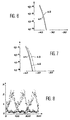
- the transmission capacity of the regenerated signal is illustrated by the curves shown on the Figures 7 and 8.
- the transmission penalty is 1.8 decibels, therefore of the same order of magnitude as the penalty for transmission over this length of a signal not regenerated.
- Filter 21 is not necessary if, as shown in figure 9, the continuous wave is introduced in arms 11 and 12 of the interferometer at a end of these arms opposite to that by which are introduced on these arms the signal to be regenerated and the clock signal respectively.
- input coupling means 13 respectively couple, as described in connection with FIG. 1, the signal input optics from arm 15 to arm 11 and the clock signal on arm 12. These signals are coupled to a first end of each of these arms.
- a second end of each of these arms is coupled by coupling means input 13 'at source 34 of wave generation continues, so that the continuous wave travels in direction inverse of the signal to be regenerated and the clock signal.
Landscapes
- Physics & Mathematics (AREA)
- Electromagnetism (AREA)
- Engineering & Computer Science (AREA)
- Computer Networks & Wireless Communication (AREA)
- Signal Processing (AREA)
- Optical Communication System (AREA)
- Glass Compositions (AREA)
- Eye Examination Apparatus (AREA)
- Developing Agents For Electrophotography (AREA)
- Optical Modulation, Optical Deflection, Nonlinear Optics, Optical Demodulation, Optical Logic Elements (AREA)
- Semiconductor Lasers (AREA)
- Electrostatic, Electromagnetic, Magneto- Strictive, And Variable-Resistance Transducers (AREA)
Abstract
Description
- les premier et second bras à un générateur d'une onde optique continue ;
- le second bras à un générateur d'un signal d'horloge du signal à régénérer
- et en ce que la sortie des moyens de couplage de sortie est porteuse du signal optique d'entrée régénéré.
- la figure 1, représente schématiquement un dispositif selon l'invention ;
- les figures 2 et 3, sont des diagrammes destinés à expliquer le fonctionnement de l'invention ;
- la figure 4, représente un dispositif expérimental destiné à tester l'invention ;
- la figure 5 comporte les parties A, B, C et D. Les parties A et B représentent respectivement la trace du signal à régénérer et son diagramme d'oeil ;
- les parties C et D, représentent la trace du signal régénérée par le dispositif selon l'invention et son diagramme d'oeil ;
- la figure 6, représente deux courbes représentant chacune le taux d'erreurs sur bit pour le signal à régénérer et pour le signal régénéré respectivement ;
- la figure 7, représente des courbes représentant chacune le taux d'erreurs sur bit pour le signal à régénérer, le signal régénéré et pour ce même signal régénéré après transmission sur une fibre mode unique standard de 31 km ;
- la figure 8 représente le diagramme d'oeil du signal régénéré transmis.
- la figure 9 représente une variante de réalisation du circuit selon l'invention représenté figure 1.
Claims (4)
- Dispositif (1) pour régénérer un signal optique d'entrée modulé en amplitude par impulsion, le dispositif comportant une structure (10) interférométrique ayant un premier (11) et un second (12) bras, un milieu optique (19,20) non linéaire étant présent sur chacun des bras (11,12), des moyens (13) de couplage d'entrée couplés auxdits premier (11) et second (12) bras, le premier (11) bras recevant au travers de ces moyens (13) de couplage d'entrée le signal optique à régénérer, des moyens de couplage (14) de sortie couplés auxdits premier (11) et second (12) bras et délivrant un signal d'interférence entre des signaux provenant du premier (11) et du second (12) bras respectivement, dispositif caractérisé en ce que la structure interférométrique est telle que sa sortie est nulle lorsqu'il n'y a pas de déphasage dynamique entre les deux bras et en ce que les moyens (13) de couplage d'entrée couplent en outre :les premier et second bras à un générateur (34) d'une onde optique continue ;le second bras (12) à un générateur (31) d'un signal d'horloge du signal à régénéreret en ce que la sortie des moyens (14) de couplage de sortie est porteuse du signal optique d'entrée régénéré.
- Dispositif selon la revendication 1, caractérisé en ce que les milieux optiques (19,20) non linéaires, sont sensibles à la puissance optique les traversant et sont constitués par des amplificateurs optiques à semi- conducteur.
- Dispositif selon l'une des revendications 1 ou 2, caractérisé en ce qu'un guide (15-18), au moins, raccordé aux moyens (13) de couplage d'entrée ou aux moyens (14) de couplage de sortie, comporte un amplificateur optique (21-24).
- Dispositif selon la revendication 2 caractérisé en ce que des moyens (22) de réglage de niveau de puissance optique sont présents entre le générateur (34) d'une onde continue et chacun des bras (11, 12), ces moyens (22) de réglage ajustant le niveau de l'onde continue à un niveau proche d'un niveau de saturation de chacun des amplificateurs optiques (19, 20) à semi conducteur présents sur chacun des bras (11, 12)de la structure interférométrique
Applications Claiming Priority (2)
| Application Number | Priority Date | Filing Date | Title |
|---|---|---|---|
| FR0000338A FR2803698B1 (fr) | 2000-01-12 | 2000-01-12 | Regeneration 3r d'un signal optique |
| FR0000338 | 2000-01-12 |
Publications (2)
| Publication Number | Publication Date |
|---|---|
| EP1117199A1 true EP1117199A1 (fr) | 2001-07-18 |
| EP1117199B1 EP1117199B1 (fr) | 2008-02-27 |
Family
ID=8845826
Family Applications (1)
| Application Number | Title | Priority Date | Filing Date |
|---|---|---|---|
| EP01400062A Expired - Lifetime EP1117199B1 (fr) | 2000-01-12 | 2001-01-11 | Régénération 3R d'un signal optique |
Country Status (6)
| Country | Link |
|---|---|
| US (1) | US6775481B2 (fr) |
| EP (1) | EP1117199B1 (fr) |
| JP (1) | JP2001251251A (fr) |
| AT (1) | ATE387762T1 (fr) |
| DE (1) | DE60132941T2 (fr) |
| FR (1) | FR2803698B1 (fr) |
Cited By (1)
| Publication number | Priority date | Publication date | Assignee | Title |
|---|---|---|---|---|
| EP1290843A2 (fr) * | 2000-06-05 | 2003-03-12 | HRL Laboratories, LLC | Procede et appareil de detection de signaux optiques |
Families Citing this family (11)
| Publication number | Priority date | Publication date | Assignee | Title |
|---|---|---|---|---|
| US6563621B2 (en) * | 2000-10-06 | 2003-05-13 | Alphion Corporation | Bit-rate and format insensitive all-optical clock extraction circuit |
| US6570697B2 (en) * | 2000-10-06 | 2003-05-27 | Alphion Corporation | Format insensitive and bit rate independent optical preprocessor |
| US6765715B1 (en) * | 2001-03-09 | 2004-07-20 | Finisar Corporation | Optical 2R/3R regeneration |
| US7203427B2 (en) * | 2001-05-15 | 2007-04-10 | Alphion Corporation | Redundant path all-optical regeneration, reshaping and wavelength conversion for enhanced yield |
| US7440179B2 (en) * | 2002-05-29 | 2008-10-21 | Alphion Corporation | SOA-MZI device fault isolation |
| GB2390243B (en) * | 2002-06-28 | 2005-11-02 | Corning Inc | Optical regenerator |
| US20040047283A1 (en) * | 2002-09-10 | 2004-03-11 | Bonwick Mark Henry | FDM signals crosstalk cancellation technique |
| US7035550B2 (en) * | 2002-12-10 | 2006-04-25 | The Trustees Of Princeton University | All-optical, 3R regeneration using the Sagnac and Mach-Zehnder versions of the terahertz optical asymmetric demultiplexer (TOAD) |
| WO2005025243A2 (fr) * | 2003-09-04 | 2005-03-17 | The Regents Of The University Of California | Regenerateurs tout optique multicanaux reconfigurables |
| US7239768B2 (en) * | 2004-06-02 | 2007-07-03 | Alphion Corporation | Photonic integrated circuit |
| US7489873B2 (en) * | 2004-12-08 | 2009-02-10 | Electronics And Telecommunications Research Institute | Optical signal retiming, reshaping, and reamplifying (3R) regeneration system having monolithically integrated Mach Zehnder interferometer and self-pulsating laser diode |
Citations (3)
| Publication number | Priority date | Publication date | Assignee | Title |
|---|---|---|---|---|
| EP0849622A2 (fr) * | 1996-12-19 | 1998-06-24 | Nortel Networks Corporation | Echantillonage tout optique par modulation d'un train d'impulsions |
| US5781326A (en) * | 1996-06-14 | 1998-07-14 | Alcatel Alsthom Compagnie Generale D'electricite | Apparatus for shaping binary optical signals, and use thereof to modify said signals |
| US5999283A (en) * | 1997-05-19 | 1999-12-07 | Roberts; Kim Byron | Optical logic devices and methods |
Family Cites Families (3)
| Publication number | Priority date | Publication date | Assignee | Title |
|---|---|---|---|---|
| GB2320635A (en) * | 1996-12-19 | 1998-06-24 | Northern Telecom Ltd | Optical timing detection using an interferometer |
| GB9712019D0 (en) * | 1997-06-09 | 1997-08-06 | Northern Telecom Ltd | Eye measurement of optical sampling |
| US6046841A (en) * | 1998-04-24 | 2000-04-04 | Mahgerefteh; Daniel | All-optical wavelength conversion system comprising an optical discriminator |
-
2000
- 2000-01-12 FR FR0000338A patent/FR2803698B1/fr not_active Expired - Fee Related
-
2001
- 2001-01-08 US US09/755,130 patent/US6775481B2/en not_active Expired - Lifetime
- 2001-01-11 AT AT01400062T patent/ATE387762T1/de not_active IP Right Cessation
- 2001-01-11 JP JP2001003261A patent/JP2001251251A/ja not_active Withdrawn
- 2001-01-11 EP EP01400062A patent/EP1117199B1/fr not_active Expired - Lifetime
- 2001-01-11 DE DE60132941T patent/DE60132941T2/de not_active Expired - Lifetime
Patent Citations (3)
| Publication number | Priority date | Publication date | Assignee | Title |
|---|---|---|---|---|
| US5781326A (en) * | 1996-06-14 | 1998-07-14 | Alcatel Alsthom Compagnie Generale D'electricite | Apparatus for shaping binary optical signals, and use thereof to modify said signals |
| EP0849622A2 (fr) * | 1996-12-19 | 1998-06-24 | Nortel Networks Corporation | Echantillonage tout optique par modulation d'un train d'impulsions |
| US5999283A (en) * | 1997-05-19 | 1999-12-07 | Roberts; Kim Byron | Optical logic devices and methods |
Non-Patent Citations (2)
| Title |
|---|
| RAYBON G ET AL.: "20 Gbit/s all-optical regeneration and wavelength conversion using SOA based interferometers", OPTICAL FIBER COMMUNICATION CONFERENCE, 1999, AND THE INTERNATIONAL CONFERENCE ON INTEGRATED OPTICS AND FIBER COMMUNICATION. OFC/IOOC'99. TECHNICAL DIGEST, vol. 4, 21 February 1999 (1999-02-21) - 26 February 1999 (1999-02-26), pages 27 - 29, XP002147998 * |
| SPIEKMAN L H ET AL: "ALL-OPTICAL MACH-ZEHNDER WAVELENGTH CONVERTER WITH MONOLITHICALLY INTEGRATED PREAMPLIFIERS", IEEE PHOTONICS TECHNOLOGY LETTERS,US,IEEE INC. NEW YORK, vol. 10, no. 8, 1 August 1998 (1998-08-01), pages 1115 - 1117, XP000769874, ISSN: 1041-1135 * |
Cited By (1)
| Publication number | Priority date | Publication date | Assignee | Title |
|---|---|---|---|---|
| EP1290843A2 (fr) * | 2000-06-05 | 2003-03-12 | HRL Laboratories, LLC | Procede et appareil de detection de signaux optiques |
Also Published As
| Publication number | Publication date |
|---|---|
| DE60132941D1 (de) | 2008-04-10 |
| JP2001251251A (ja) | 2001-09-14 |
| US20010028492A1 (en) | 2001-10-11 |
| EP1117199B1 (fr) | 2008-02-27 |
| DE60132941T2 (de) | 2009-02-26 |
| US6775481B2 (en) | 2004-08-10 |
| FR2803698B1 (fr) | 2003-06-27 |
| ATE387762T1 (de) | 2008-03-15 |
| FR2803698A1 (fr) | 2001-07-13 |
Similar Documents
| Publication | Publication Date | Title |
|---|---|---|
| CA2165689C (fr) | Procede de transmission optique presentant une sensibilite reduite a la dispersion; dispositif et systeme de transmission pour la mise en oeuvre de ce procede | |
| EP0817408B1 (fr) | Récepteur pour système de transmissions de signaux numériques par voie optique | |
| EP1117199B1 (fr) | Régénération 3R d'un signal optique | |
| FR2642922A1 (fr) | Dispositif de communication sur spectre disperse | |
| FR2652215A1 (fr) | Procede de codage d'un signal numerique, codeur et decodeur pour la mise en óoeuvre de ce procede, procede de regeneration et regenerateur correspondant. | |
| FR2681203A1 (fr) | Systeme de transmission optique, et emetteur et recepteur optiques. | |
| EP0813097B1 (fr) | Dispositif de mise en forme de signaux optiques binaires et son utilisation pour modifier lesdits signaux | |
| EP1811679B1 (fr) | Chaîne de réception de signaux | |
| FR2768231A1 (fr) | Structure interferometrique integree | |
| EP1511200B1 (fr) | Dispositif de régénération d'un signal optique et procédé correspondant. | |
| EP0818896A1 (fr) | Système de transmission optique de données en format soliton | |
| EP1311079B1 (fr) | Système de transmission de signal optique à phase contrôlée | |
| EP1544669B1 (fr) | Dispositif de régéneration d'un signal optique, utilisation d'un tel dispositif et installation comportant un tel dispositif | |
| FR2797331A1 (fr) | Differenciateur optique | |
| EP0031774B1 (fr) | Procédé de modulation à seize états du type MAMSK pour système de transmission de données numériques et modulateurs et démodulateur | |
| EP0746070B1 (fr) | Procédé et dispositif pour combiner des signaux optiques | |
| FR2681747A1 (fr) | Dispositif de restitution d'horloge utilisant un filtre a onde de surface. | |
| EP1314267A1 (fr) | Regenerateur tout-optique pour signaux multiplexes en longuer d'onde | |
| EP1286483A2 (fr) | Modulateur optique amélioré permettant une optimisation de la modulation NRZ | |
| EP0152854A1 (fr) | Procédé et dispositif de détection d'erreur dans un train d'informations binaires exprimées selon le code CMI | |
| WO2006077321A1 (fr) | Dispositif et procede pour la conversion optique de longueurs d'onde a partir d'un modulateur a electroabsorption | |
| WO2005112311A1 (fr) | Signal optique numerique de communication a « chirp » non lineaire reduit, systeme et procede correspondants. | |
| FR2544937A1 (fr) | Circuit demodulateur de signal biphase | |
| JP2005064953A (ja) | マーク率評価装置 |
Legal Events
| Date | Code | Title | Description |
|---|---|---|---|
| PUAI | Public reference made under article 153(3) epc to a published international application that has entered the european phase |
Free format text: ORIGINAL CODE: 0009012 |
|
| AK | Designated contracting states |
Kind code of ref document: A1 Designated state(s): AT BE CH CY DE DK ES FI FR GB GR IE IT LI LU MC NL PT SE TR |
|
| AX | Request for extension of the european patent |
Free format text: AL;LT;LV;MK;RO;SI |
|
| 17P | Request for examination filed |
Effective date: 20011219 |
|
| AKX | Designation fees paid |
Free format text: AT BE CH CY DE DK ES FI FR GB GR IE IT LI LU MC NL PT SE TR |
|
| 17Q | First examination report despatched |
Effective date: 20061201 |
|
| RAP1 | Party data changed (applicant data changed or rights of an application transferred) |
Owner name: ALCATEL LUCENT |
|
| GRAP | Despatch of communication of intention to grant a patent |
Free format text: ORIGINAL CODE: EPIDOSNIGR1 |
|
| GRAS | Grant fee paid |
Free format text: ORIGINAL CODE: EPIDOSNIGR3 |
|
| GRAA | (expected) grant |
Free format text: ORIGINAL CODE: 0009210 |
|
| AK | Designated contracting states |
Kind code of ref document: B1 Designated state(s): AT BE CH CY DE DK ES FI FR GB GR IE IT LI LU MC NL PT SE TR |
|
| REG | Reference to a national code |
Ref country code: GB Ref legal event code: FG4D Free format text: NOT ENGLISH |
|
| RIN1 | Information on inventor provided before grant (corrected) |
Inventor name: WOLFSON, DAVID Inventor name: GUERBER, PATRICIA Inventor name: LAVIGNE, BRUNO Inventor name: JANZ, CHRISTOPHER Inventor name: FJELDE, TINA Inventor name: KLOCH, ALLAN |
|
| REG | Reference to a national code |
Ref country code: CH Ref legal event code: EP |
|
| REG | Reference to a national code |
Ref country code: IE Ref legal event code: FG4D Free format text: LANGUAGE OF EP DOCUMENT: FRENCH |
|
| REF | Corresponds to: |
Ref document number: 60132941 Country of ref document: DE Date of ref document: 20080410 Kind code of ref document: P |
|
| GBT | Gb: translation of ep patent filed (gb section 77(6)(a)/1977) |
Effective date: 20080413 |
|
| PG25 | Lapsed in a contracting state [announced via postgrant information from national office to epo] |
Ref country code: FI Free format text: LAPSE BECAUSE OF FAILURE TO SUBMIT A TRANSLATION OF THE DESCRIPTION OR TO PAY THE FEE WITHIN THE PRESCRIBED TIME-LIMIT Effective date: 20080227 Ref country code: ES Free format text: LAPSE BECAUSE OF FAILURE TO SUBMIT A TRANSLATION OF THE DESCRIPTION OR TO PAY THE FEE WITHIN THE PRESCRIBED TIME-LIMIT Effective date: 20080607 |
|
| NLV1 | Nl: lapsed or annulled due to failure to fulfill the requirements of art. 29p and 29m of the patents act | ||
| PG25 | Lapsed in a contracting state [announced via postgrant information from national office to epo] |
Ref country code: AT Free format text: LAPSE BECAUSE OF FAILURE TO SUBMIT A TRANSLATION OF THE DESCRIPTION OR TO PAY THE FEE WITHIN THE PRESCRIBED TIME-LIMIT Effective date: 20080227 |
|
| REG | Reference to a national code |
Ref country code: IE Ref legal event code: FD4D |
|
| PG25 | Lapsed in a contracting state [announced via postgrant information from national office to epo] |
Ref country code: DK Free format text: LAPSE BECAUSE OF FAILURE TO SUBMIT A TRANSLATION OF THE DESCRIPTION OR TO PAY THE FEE WITHIN THE PRESCRIBED TIME-LIMIT Effective date: 20080227 Ref country code: IE Free format text: LAPSE BECAUSE OF FAILURE TO SUBMIT A TRANSLATION OF THE DESCRIPTION OR TO PAY THE FEE WITHIN THE PRESCRIBED TIME-LIMIT Effective date: 20080227 Ref country code: NL Free format text: LAPSE BECAUSE OF FAILURE TO SUBMIT A TRANSLATION OF THE DESCRIPTION OR TO PAY THE FEE WITHIN THE PRESCRIBED TIME-LIMIT Effective date: 20080227 Ref country code: PT Free format text: LAPSE BECAUSE OF FAILURE TO SUBMIT A TRANSLATION OF THE DESCRIPTION OR TO PAY THE FEE WITHIN THE PRESCRIBED TIME-LIMIT Effective date: 20080721 Ref country code: SE Free format text: LAPSE BECAUSE OF FAILURE TO SUBMIT A TRANSLATION OF THE DESCRIPTION OR TO PAY THE FEE WITHIN THE PRESCRIBED TIME-LIMIT Effective date: 20080527 |
|
| PLBE | No opposition filed within time limit |
Free format text: ORIGINAL CODE: 0009261 |
|
| STAA | Information on the status of an ep patent application or granted ep patent |
Free format text: STATUS: NO OPPOSITION FILED WITHIN TIME LIMIT |
|
| 26N | No opposition filed |
Effective date: 20081128 |
|
| PG25 | Lapsed in a contracting state [announced via postgrant information from national office to epo] |
Ref country code: CY Free format text: LAPSE BECAUSE OF FAILURE TO SUBMIT A TRANSLATION OF THE DESCRIPTION OR TO PAY THE FEE WITHIN THE PRESCRIBED TIME-LIMIT Effective date: 20080227 |
|
| PG25 | Lapsed in a contracting state [announced via postgrant information from national office to epo] |
Ref country code: MC Free format text: LAPSE BECAUSE OF NON-PAYMENT OF DUE FEES Effective date: 20090131 Ref country code: IT Free format text: LAPSE BECAUSE OF FAILURE TO SUBMIT A TRANSLATION OF THE DESCRIPTION OR TO PAY THE FEE WITHIN THE PRESCRIBED TIME-LIMIT Effective date: 20080227 |
|
| REG | Reference to a national code |
Ref country code: CH Ref legal event code: PL |
|
| PG25 | Lapsed in a contracting state [announced via postgrant information from national office to epo] |
Ref country code: LI Free format text: LAPSE BECAUSE OF NON-PAYMENT OF DUE FEES Effective date: 20090131 Ref country code: CH Free format text: LAPSE BECAUSE OF NON-PAYMENT OF DUE FEES Effective date: 20090131 |
|
| PG25 | Lapsed in a contracting state [announced via postgrant information from national office to epo] |
Ref country code: BE Free format text: LAPSE BECAUSE OF NON-PAYMENT OF DUE FEES Effective date: 20090131 |
|
| PG25 | Lapsed in a contracting state [announced via postgrant information from national office to epo] |
Ref country code: GR Free format text: LAPSE BECAUSE OF FAILURE TO SUBMIT A TRANSLATION OF THE DESCRIPTION OR TO PAY THE FEE WITHIN THE PRESCRIBED TIME-LIMIT Effective date: 20080528 |
|
| PG25 | Lapsed in a contracting state [announced via postgrant information from national office to epo] |
Ref country code: LU Free format text: LAPSE BECAUSE OF NON-PAYMENT OF DUE FEES Effective date: 20090111 |
|
| PG25 | Lapsed in a contracting state [announced via postgrant information from national office to epo] |
Ref country code: TR Free format text: LAPSE BECAUSE OF FAILURE TO SUBMIT A TRANSLATION OF THE DESCRIPTION OR TO PAY THE FEE WITHIN THE PRESCRIBED TIME-LIMIT Effective date: 20080227 |
|
| REG | Reference to a national code |
Ref country code: FR Ref legal event code: GC Effective date: 20131018 |
|
| REG | Reference to a national code |
Ref country code: FR Ref legal event code: PLFP Year of fee payment: 15 |
|
| REG | Reference to a national code |
Ref country code: FR Ref legal event code: CA Effective date: 20150521 |
|
| REG | Reference to a national code |
Ref country code: FR Ref legal event code: CA Effective date: 20150521 |
|
| REG | Reference to a national code |
Ref country code: FR Ref legal event code: PLFP Year of fee payment: 16 |
|
| REG | Reference to a national code |
Ref country code: FR Ref legal event code: PLFP Year of fee payment: 17 |
|
| PGFP | Annual fee paid to national office [announced via postgrant information from national office to epo] |
Ref country code: DE Payment date: 20170120 Year of fee payment: 17 Ref country code: FR Payment date: 20170120 Year of fee payment: 17 |
|
| PGFP | Annual fee paid to national office [announced via postgrant information from national office to epo] |
Ref country code: GB Payment date: 20170119 Year of fee payment: 17 |
|
| REG | Reference to a national code |
Ref country code: DE Ref legal event code: R119 Ref document number: 60132941 Country of ref document: DE |
|
| GBPC | Gb: european patent ceased through non-payment of renewal fee |
Effective date: 20180111 |
|
| PG25 | Lapsed in a contracting state [announced via postgrant information from national office to epo] |
Ref country code: DE Free format text: LAPSE BECAUSE OF NON-PAYMENT OF DUE FEES Effective date: 20180801 Ref country code: FR Free format text: LAPSE BECAUSE OF NON-PAYMENT OF DUE FEES Effective date: 20180131 |
|
| REG | Reference to a national code |
Ref country code: FR Ref legal event code: ST Effective date: 20180928 |
|
| PG25 | Lapsed in a contracting state [announced via postgrant information from national office to epo] |
Ref country code: GB Free format text: LAPSE BECAUSE OF NON-PAYMENT OF DUE FEES Effective date: 20180111 |