EP1117128A2 - Method and apparatus for orienting substrates - Google Patents
Method and apparatus for orienting substrates Download PDFInfo
- Publication number
- EP1117128A2 EP1117128A2 EP01300056A EP01300056A EP1117128A2 EP 1117128 A2 EP1117128 A2 EP 1117128A2 EP 01300056 A EP01300056 A EP 01300056A EP 01300056 A EP01300056 A EP 01300056A EP 1117128 A2 EP1117128 A2 EP 1117128A2
- Authority
- EP
- European Patent Office
- Prior art keywords
- substrate
- som
- handler
- rotatable
- support
- Prior art date
- Legal status (The legal status is an assumption and is not a legal conclusion. Google has not performed a legal analysis and makes no representation as to the accuracy of the status listed.)
- Withdrawn
Links
Images



Classifications
-
- H—ELECTRICITY
- H10—SEMICONDUCTOR DEVICES; ELECTRIC SOLID-STATE DEVICES NOT OTHERWISE PROVIDED FOR
- H10P—GENERIC PROCESSES OR APPARATUS FOR THE MANUFACTURE OR TREATMENT OF DEVICES COVERED BY CLASS H10
- H10P72/00—Handling or holding of wafers, substrates or devices during manufacture or treatment thereof
- H10P72/50—Handling or holding of wafers, substrates or devices during manufacture or treatment thereof for positioning, orientation or alignment
-
- H—ELECTRICITY
- H10—SEMICONDUCTOR DEVICES; ELECTRIC SOLID-STATE DEVICES NOT OTHERWISE PROVIDED FOR
- H10P—GENERIC PROCESSES OR APPARATUS FOR THE MANUFACTURE OR TREATMENT OF DEVICES COVERED BY CLASS H10
- H10P72/00—Handling or holding of wafers, substrates or devices during manufacture or treatment thereof
- H10P72/50—Handling or holding of wafers, substrates or devices during manufacture or treatment thereof for positioning, orientation or alignment
- H10P72/53—Handling or holding of wafers, substrates or devices during manufacture or treatment thereof for positioning, orientation or alignment using optical controlling means
-
- Y—GENERAL TAGGING OF NEW TECHNOLOGICAL DEVELOPMENTS; GENERAL TAGGING OF CROSS-SECTIONAL TECHNOLOGIES SPANNING OVER SEVERAL SECTIONS OF THE IPC; TECHNICAL SUBJECTS COVERED BY FORMER USPC CROSS-REFERENCE ART COLLECTIONS [XRACs] AND DIGESTS
- Y10—TECHNICAL SUBJECTS COVERED BY FORMER USPC
- Y10S—TECHNICAL SUBJECTS COVERED BY FORMER USPC CROSS-REFERENCE ART COLLECTIONS [XRACs] AND DIGESTS
- Y10S414/00—Material or article handling
- Y10S414/135—Associated with semiconductor wafer handling
- Y10S414/136—Associated with semiconductor wafer handling including wafer orienting means
-
- Y—GENERAL TAGGING OF NEW TECHNOLOGICAL DEVELOPMENTS; GENERAL TAGGING OF CROSS-SECTIONAL TECHNOLOGIES SPANNING OVER SEVERAL SECTIONS OF THE IPC; TECHNICAL SUBJECTS COVERED BY FORMER USPC CROSS-REFERENCE ART COLLECTIONS [XRACs] AND DIGESTS
- Y10—TECHNICAL SUBJECTS COVERED BY FORMER USPC
- Y10S—TECHNICAL SUBJECTS COVERED BY FORMER USPC CROSS-REFERENCE ART COLLECTIONS [XRACs] AND DIGESTS
- Y10S414/00—Material or article handling
- Y10S414/135—Associated with semiconductor wafer handling
- Y10S414/137—Associated with semiconductor wafer handling including means for charging or discharging wafer cassette
- Y10S414/138—Wafers positioned vertically within cassette
Definitions
- the present invention relates to substrate processing (e.g., semiconductor device fabrication, flat panel display fabrication, etc.) and more specifically to a method and apparatus for orienting substrates (e.g., semiconductor wafers, glass substrates for flat panel displays, etc.).
- substrate processing e.g., semiconductor device fabrication, flat panel display fabrication, etc.
- substrates e.g., semiconductor wafers, glass substrates for flat panel displays, etc.
- Proper alignment or "orientation" of substrates is often required during substrate processing.
- proper semiconductor wafer orientation is required during processing steps sensitive to wafer orientation (e.g., lithographic processes, masking steps, etc), for reading information scribed on a wafer's backside (e.g., lot number wafer aerial number, etc.) and the like.
- wafer orientation e.g., lithographic processes, masking steps, etc
- information scribed on a wafer's backside e.g., lot number wafer aerial number, etc.
- semiconductor wafers are provided with a flattened edge region termed a "flat" along an otherwise rounded wafer edge, or a small portion of a wafer's edge is removed to form a "notch" therein.
- Conventional wafer orientation devices typically comprise a platform having a rotatable surface, and a wafer orientation sensor (e.g., an optical sensor) positioned a small distance above the platform.
- a wafer orientation sensor e.g., an optical sensor
- a wafer is placed on the rotatable surface of the platform, the rotatable surface is rotated (so as to rotate the wafer) and the wafer position sensor is employed to identify when a flat or notch of the wafer is in a predetermined position.
- the wafer position sensor then transmits this information to the platform to cease wafer rotation.
- wafer transfer to, wafer orientation by, and wafer transfer from conventional wafer orienting devices follows the same sequence: 1) a wafer handler extracts a first wafer from a multi-slot wafer carrier and transports the first wafer to the wafer orienting device; 2) the wafer orienting device orients the first wafer; and 3) the wafer handler returns the oriented first wafer to the multi-slot wafer carrier. Thereafter the sequence repeats and the wafer handler extracts a second wafer from the multi-slot wafer carrier and transports the second wafer to the wafer orienting device, etc.
- a wafer orienter that can simultaneously orient multiple substrates while occupying a small footprint.
- a small footprint preferably is achieved primarily by employing equipment already present within moat device fabrication tools (e.g., so that the equipment does not consume any additional space) and by implementing the orienter in a compact, vertically stacked configuration. Simultaneous substrate orientation significantly increases substrate throughput, thereby decreasing cost per unit substrate processed. A small footprint further decreases coat per unit substrate processed by reducing cleanroom space requirements.
- a multiple substrate orienter in accordance with the present invention, includes a rotatable substrate handler having a plurality of substrate support portions, each adapted to support a substrate.
- the multiple substrate orienter also includes a plurality of stacked substrate supports, each adapted to support a substrate.
- a plurality of substrate orientation marking (SOM) detectors are provided, and each SOM detector is coupled to a different one of the substrate supports and is adapted to identify a presence of an SOM (e.g., a wafer flat or notch) of a substrate positioned close enough to the SOM detector to allow SOM detection by the SOM detector.
- SOM substrate orientation marking
- the multiple substrate orienter further includes a plurality of lift and lower mechanisms, each lift and lower mechanism coupled to a different one of the substrate supports and adapted to individually lift and lower the substrate support to which the lift and lower mechanism is coupled.
- each lift and lower mechanism may be coupled to a different one of the substrate support portions of the rotatable substrate handler and adapted to individually lift and lower the substrate support portion to which the lift and lower mechanism is coupled.
- the multiple substrate orienter includes a controller coupled to the rotatable substrate handler, to the plurality of SOM detectors and to the plurality of lift and lower mechanisms.
- the controller preferably has program code adapted to simultaneously rough orient a plurality of substrates loaded onto the substrate support portions of the rotatable substrate handler, and to individually fine orient each rough oriented substrate.
- to "simultaneously rough orient a plurality of substrates” means to perform at least one portion of a rough orientation process simultaneously on the plurality of substrates, although each and every portion of the rough orientation process need not be performed simultaneously on all of the substrates.
- To "individually fine orient each rough oriented substrate” means to fine orient each rough oriented substrate one substrate at a time (e.g., not simultaneously).
- a substrate orienter in another aspect of the invention, is provided the rotatable substrate handler of which has a single substrate support portion adapted to support a single substrate.
- Both aspects of the invention employ the substrate handler's rotational capability for substrate orienting, and both aspects perform a high speed rough orient which considerably reduces the time required for substrate orienting, as compared to conventional methods.
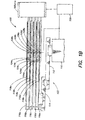
- FIGS. 1A and 1B are a top plan view and a side elevational view, respectively, of an inventive multiple substrate orienter 100 configured in accordance with the present invention.
- the multiple substrate orienter 100 is described with reference to semiconductor wafer handling equipment.
- the multiple substrate orienter 100 may be adapted to employ other substrate handling equipment (e.g., glass substrate handling equipment for flat panel displays, etc.),
- the multiple substrate orienter 100 comprises a rotatable substrate handler 102, a plurality of vertically stacked substrate supports 104a-e and a plurality of lift and lower mechanisms 106a-e coupled to the substrate supports 104a-e.
- a substrate orientation marking (SOM) detector 108a-e e.g., a detector for determining the presence of a wafer notch or flat
- SOM substrate orientation marking
- a controller 109 is coupled to the rotatable substrate handler 102, to the lift and lower mechanisms 106a-e and to the SOM detectors 108a-e and includes program code (e.g., software) for controlling the operation of the multiple substrate orienter 100 as described below with reference to FIG. 3.
- the controller may comprise, for example, a dedicated controller for the multiple substrate orienter 100, a remote computer system for running a fabrication process, a manufacturing execution system, etc.
- the rotatable substrate handler 102 includes a base 110 about which the entire wafer handler may rotate, a first extension 112 rotatably coupled to the base 110, a second extension 114 rotatably coupled to the first extension 112 and a plurality of substrate support portions 116a-e rotatably coupled to the second extension 114 but preferably fixedly coupled to one another so that the substrate support portions 116a-e move together as a unit.
- Each substrate support portion 116a-e preferably comprises a blade configuration (as shown by the substrate support portion 116a of FIG. 1A) having a width less than a diameter of a substrate 118a-e supported thereon.
- Each substrate support portion 116a-e further includes a gripper mechanism 120a-e for pressing against an edge of each substrate 118a-a to secure each substrate 118a-e during transport and/or to center each substrate 118a-e as is known in the art.
- Each substrate support 104a-e preferably is configured to support a substrate near an edge of the substrate, such as via a first and second edge support 122a-e, 124a-e (FIG. 1A). In this manner, substrates 118a-e may be placed on the substrate supports 104a-e by the substrate support portions 116a-e without the substrate support portions 116a-e contacting or otherwise interfering with the substrate supports 104a-e.
- the lift and lower mechanisms 106a-e are configured to individually lift and lower each substrate support 104a-e (e.g., each substrate support may be raised and lowered independently of the other substrate supports), and preferably comprise computer controllable, pneumatic cylinders that raise/lower under the influence of compressed air as is well known in the art.
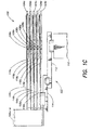
- the lift and lower mechanisms 106a-e alternatively may be coupled to the substrate support portions 116a-e (FIG. 1C) so as to allow each of the substrate support portions 116a-e to be individually raised and lowered instead of the substrate supports 104a-e.
- the SOM detectors 109a-e may comprise any known detector for determining the presence or absence of a substrate orientation marking. However, for substrates employing a flat or a notch, the SOM detectors 108a-e preferably comprise fiber-optic-based sensors coupled to the second edge supports 124a-e of the substrate supports 104a-e as shown in FIGS. 1A and 1B.
- FIG. 2A is a perspective view of the preferred SOM detector 108a of FIG. 1A when the substrate 118a comprises a notch 126a as a substrate orientation marking.
- the notch 126a typically has sidewalls at a 45° angle to a substrate diameter.
- the SOM detector 108a comprises a laser source 128 (e.g., a laser diode such as a GaAs-based semiconductor laser diode) that outputs a laser beam 130.
- the laser beam 130 is directed toward the notch 126a via a first fiber optic cable 132 positioned (via a fiber optic support 134) so that the laser beam 130 exits the first fiber optic cable 132 and strikes the notch 126a if the substrate 118a is aligned with the detector 108a as shown.
- the laser beam 130 preferably strikes the notch 126a approximately perpendicularly.
- a "collectable" reflected laser beam 136 is generated.
- the reflected laser beam 136 is collected by a second fiber optic cable 138 (also supported by the fiber optic support 134) and is transmitted thereby to a photodetector 140 (e.g., a silicon, junction based photodiode).
- a photodetector 140 e.g., a silicon, junction based photodiode.
- a photodetector 140 e.g., a silicon, junction based photodiode
- the photodetector 140 detects reflected light; otherwise, when the substrate 118a is oriented so that the laser beam 130 strikes another edge portion of the substrate 118a, the photodetector 140 does not detect reflected light.
- the SOM of the substrate 118a thereby is easily found by aligning the substrate 118a with the SOM detector 108a so that the laser beam 130 strikes the notch 126a.
- the SOM detector 108a also may be configured so that reflected light is not detected by the photodetector 140 when the substrate 118a's SOM is aligned with the SOM detector 108a but is detected when the substrate 118a's SOM is not aligned with the SOM detector 108a.
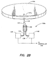
- FIG. 2B shows the SOM detector 108a positioned so that a collectible reflected light beam 136 is generated only when an SOM (shown as a flat 142a although a notch may be similarly detected) of the substrate 118a is not aligned with the SOM detector 108a.
- the SOM detector 108a When the SOM of the substrate 118a is aligned with the SOM detector 108a, no reflected beam is generated as the laser beam 130 does not strike the substrate 118a. Note that the SOM detector 108a may be positioned above or below the substrate 118a.
- FIG. 3 is a flowchart 300 of the preferred operation of the multiple substrate orienter 100.
- the controller 109 comprises program code for controlling the multiple substrate orienter 100 in accordance with the flowchart 300.
- step 301 the operation of the multiple substrate orienter 100 begins.
- a substrate is loaded onto each substrate support portion 116a-e of the rotatable substrate handler 102.
- the rotatable substrate handler 102 may simultaneously load the substrates 118a-e onto the substrate support portions 116a-e by extending the first extension 112, the second extension 114 and/or the substrate support portions 116a-e so as to position the substrate support portions 116a-e under the substrates 118a-e (stored within a substrate carrier (not shown)), and by indexing the substrate carrier to lower the substrates 118a-e onto the substrate support portions 116a-e.
- step 303 the first extension 112, the second extension 114 and/or the substrate support portions 116a-e retract as shown in FIGS. 1A and 1B to position each substrate 118a-e supported by the substrate support portions 116a-e above a different one of the substrate supports 104a-e.
- step 304 the rotatable substrate handler 102 is rotated by a pre-determined amount, preferably by about 90° as limited primarily by contact between the substrate support portions 116a-e and the substrate supports 104a-e.
- the presence or absence of a substrate orientation marking is detected for each substrate 118a-e by employing the SOM detectors 108a-e.
- the controller 109 monitors the photodetector 140 (e,g., via a photocurrent associated therewith) for either a presence or absence of detected light, depending on whether the configuration of FIG. 2A or the configuration of FIG. 2B is employed. If an SOM is detected for one of the substrates 118a-e, the controller 109 stores this information and preferably stores the angle the substrate is rotated past alignment with the SOM detector which detected the SOM.
- those substrates for which an SOM is detected are "rough oriented", that is the controller 109 possesses information regarding the position of the substrate's SOM relative to an SOM detector (e.g., the SOM is within a certain number of degrees beyond the SOM detector).
- the rough oriented substrates may then (as described below with reference to steps 306-308) be supported by the substrate supports 104a-e while the remaining substrates 118a-e are rotated and rough oriented.
- each substrate 118a-e is transferred to a different one of the substrate supports 104a-e.
- the lift and lower mechanisms 106a-e may simultaneously or sequentially lift each of the substrate supports 104a-e a sufficient distance to transfer each substrate 118a-e onto a different one of the substrate supports 104a-e.
- the controller 109 identifies the substrates for which an SOM has been detected (e.g., which substrates have been "completely" rough oriented) and the substrates for which an SOM has not been detected.
- the rotatable substrate handler 102 is rotated preferably in the opposite direction by the pre-determined amount (e.g., by about 90°) to reset the position of the rotatable substrate handler 102 for future rotations.
- the pre-determined amount e.g., by about 90°
- each substrate for which an SOM has not been detected is transferred to a substrate support portion of the rotatable substrate handler 102.
- each substrate support 104a-e which supports a substrate for which an SOM has not been detected is simultaneously or sequentially lowered (via the appropriate lift and lower mechanism 106a-e) a sufficient distance to transfer the substrate onto a substrate support portion of the rotatable substrate handler 102.
- Each substrate support 104a-e which supports a substrate for which an SOM has been detected is not lowered so that the substrate supported thereby is not rotated further during future rotations of the rotatable wafer handler 102.
- steps 304-308 are repeated until in step 307 an SOM has been detected for each of the substrates 118a-e.
- each substrate is "simultaneously" (and preferably very rapidly) rough oriented to within a pre-determined angular distance (e.g., within 90°) of alignment with an SOM detector 108a-e.
- each substrate 118a-e is individually "fine oriented".
- the first substrate 118a is individually transferred to the first substrate support portion 116a of the rotatable substrate handler 102 (e.g., by lowering the first substrate support 104a with the first lift and lower mechanism 106a a sufficient distance to transfer the first substrate 118a onto the first substrate support portion 116a) .
- the rotatable substrate handler 102 is rotated (e.g., preferably at a slower rate than the rotation rate employed during rough orientation to allow for more precise alignment, and typically in the opposite rotation direction to the rough orient direction) until the SOM of the first substrate 118a is aligned with the first SOM detector 108a (e.g., as signified by the reflected light measured by the photodetector 140).
- the first substrate 118a "fine oriented"
- the first substrate 118a is transferred back to the first substrate support 104a (via the first lift and lower mechanism 106a) and the above process is repeated for the remaining substrates 118b-e to individually fine orient these substrates.
- the operation of the multiple substrate orienter 100 ends in step 310.
- the oriented substrates 118a-e may be transferred to various processing chambers (not shown) via the rotatable substrate handler 102 or via another transfer mechanism for subsequent processing.
- a significant advantage of the multiple substrate orienter 100 is that it "simultaneously" orients multiple substrates while occupying a small footprint.
- Most conventional semiconductor processing tools employ a rotatable wafer handler (e.g., such as the rotatable substrate handler 102) which may be employed for wafer orientation as described herein.
- the multiple substrate orienter 100 may be formed within a very small footprint.
- simultaneous orientation of multiple substrates significantly increases substrate throughput when compared to conventional, single substrate orientation techniques, thereby decreasing cost per unit substrate processed.
- a small footprint further decreases cost per unit substrate processed by reducing cleanroom space requirements.
- the multiple substrate orienter 100 has been described with reference to simultaneously orienting five substrates, it will be understood that any number of substrates (including only one substrate) may be so oriented.
- the lift and lower mechanisms 106a-e may be coupled to the substrate support portions 116a-e (as shown in FIG. 1C) rather than to the substrate supports 104a-e (as shown in FIGS.
- the substrate support portions 116a-e then may be lifted/lowered to perform the various individual/simultaneous substrate transfer operations described herein (e.g., substrate transfers between the substrate support portions 116a-a of the substrate handler and the substrate supports 104a-e).
- substrate transfers between the substrate support portions 116a-a of the substrate handler and the substrate supports 104a-e When only a single substrate is to be so oriented, the entire substrate handler may be lifted/lowered rather than just the substrate support portion and during the rough orient the substrate rotation may be stopped as soon as possible after SOM detection, which will result in faster fine orient times.
- an extendable arm-type substrate handler is preferred, other types of substrate handlers may be employed (e.g., frog-leg type robots, etc.) as will be apparent to those of ordinary skill in the art.
- the specific configuration of the substrate supports may vary as will be apparent to those of ordinary skill in the art.
Landscapes
- Container, Conveyance, Adherence, Positioning, Of Wafer (AREA)
Abstract
A multiple substrate orienter (100) is provided
that includes a rotatable substrate handler (102)
having a plurality of substrate support portions
(104a-e), each adapted to support a substrate. The
multiple substrate orienter also includes a plurality
of stacked substrate supports, each adapted to support
a substrate. A plurality of substrate orientation
marking (SOM) detectors (108a-e) are provided, and
each SOM detector is coupled to a different one of the
substrate supports and is adapted to identify a
presence of an SOM of a substrate positioned close
enough to the SOM detector to allow SOM detection by
the SOM detector. The multiple substrate orienter
further includes a plurality of lift and lower
mechanisms (106a-e), each lift and lower mechanism
coupled to a different one of the substrate supports
and adapted to individually lift and lower the
substrate support to which the lift and lower
mechanism is coupled. Alternatively, each lift and
lower mechanism may be coupled to a different one of
the substrate support portions of the rotatable
substrate handler and adapted to individually lift and
lower the substrate support portion to which the lift
and lower mechanism is coupled. Preferably the
multiple substrate orienter includes a controller
(109) having program code adapted to simultaneously
rough orient a plurality of substrates loaded onto the
substrate support portions of the substrate handler,
and to individually fine orient each rough oriented
substrate. In further aspects of the invention, a
substrate orienter capable or orienting one or more
substrates is provided, as are methods for orienting
substrates as described above.
Description
- The present invention relates to substrate processing (e.g., semiconductor device fabrication, flat panel display fabrication, etc.) and more specifically to a method and apparatus for orienting substrates (e.g., semiconductor wafers, glass substrates for flat panel displays, etc.).
- Proper alignment or "orientation" of substrates is often required during substrate processing. For example, proper semiconductor wafer orientation is required during processing steps sensitive to wafer orientation (e.g., lithographic processes, masking steps, etc), for reading information scribed on a wafer's backside (e.g., lot number wafer aerial number, etc.) and the like. Accordingly, to identify wafer orientation, semiconductor wafers are provided with a flattened edge region termed a "flat" along an otherwise rounded wafer edge, or a small portion of a wafer's edge is removed to form a "notch" therein.
- Conventional wafer orientation devices typically comprise a platform having a rotatable surface, and a wafer orientation sensor (e.g., an optical sensor) positioned a small distance above the platform. To achieve a desired wafer orientation, a wafer is placed on the rotatable surface of the platform, the rotatable surface is rotated (so as to rotate the wafer) and the wafer position sensor is employed to identify when a flat or notch of the wafer is in a predetermined position. The wafer position sensor then transmits this information to the platform to cease wafer rotation. Accordingly, wafer transfer to, wafer orientation by, and wafer transfer from conventional wafer orienting devices follows the same sequence: 1) a wafer handler extracts a first wafer from a multi-slot wafer carrier and transports the first wafer to the wafer orienting device; 2) the wafer orienting device orients the first wafer; and 3) the wafer handler returns the oriented first wafer to the multi-slot wafer carrier. Thereafter the sequence repeats and the wafer handler extracts a second wafer from the multi-slot wafer carrier and transports the second wafer to the wafer orienting device, etc.
- As indicated by the sequence described above, conventional wafer orienting devices allow only one wafer to be oriented at a time. Such operation reduces throughput and increases wafer processing costs. Further, expensive and large footprint orienting equipment (e.g., a separate wafer platform, a motor required for rotation thereof, etc.) is also required. Accordingly a need exists for an improved wafer orienting device.
- To address the needs of the prior art, a wafer orienter is provided that can simultaneously orient multiple substrates while occupying a small footprint. A small footprint preferably is achieved primarily by employing equipment already present within moat device fabrication tools (e.g., so that the equipment does not consume any additional space) and by implementing the orienter in a compact, vertically stacked configuration. Simultaneous substrate orientation significantly increases substrate throughput, thereby decreasing cost per unit substrate processed. A small footprint further decreases coat per unit substrate processed by reducing cleanroom space requirements.
- In accordance with the present invention, a multiple substrate orienter is provided that includes a rotatable substrate handler having a plurality of substrate support portions, each adapted to support a substrate. The multiple substrate orienter also includes a plurality of stacked substrate supports, each adapted to support a substrate. A plurality of substrate orientation marking (SOM) detectors are provided, and each SOM detector is coupled to a different one of the substrate supports and is adapted to identify a presence of an SOM (e.g., a wafer flat or notch) of a substrate positioned close enough to the SOM detector to allow SOM detection by the SOM detector. The multiple substrate orienter further includes a plurality of lift and lower mechanisms, each lift and lower mechanism coupled to a different one of the substrate supports and adapted to individually lift and lower the substrate support to which the lift and lower mechanism is coupled. Alternatively, each lift and lower mechanism may be coupled to a different one of the substrate support portions of the rotatable substrate handler and adapted to individually lift and lower the substrate support portion to which the lift and lower mechanism is coupled.
- Preferably the multiple substrate orienter includes a controller coupled to the rotatable substrate handler, to the plurality of SOM detectors and to the plurality of lift and lower mechanisms. The controller preferably has program code adapted to simultaneously rough orient a plurality of substrates loaded onto the substrate support portions of the rotatable substrate handler, and to individually fine orient each rough oriented substrate. As used herein, to "simultaneously rough orient a plurality of substrates" means to perform at least one portion of a rough orientation process simultaneously on the plurality of substrates, although each and every portion of the rough orientation process need not be performed simultaneously on all of the substrates. To "individually fine orient each rough oriented substrate" means to fine orient each rough oriented substrate one substrate at a time (e.g., not simultaneously).
- In another aspect of the invention, a substrate orienter is provided the rotatable substrate handler of which has a single substrate support portion adapted to support a single substrate. Both aspects of the invention employ the substrate handler's rotational capability for substrate orienting, and both aspects perform a high speed rough orient which considerably reduces the time required for substrate orienting, as compared to conventional methods.
- Other objects, features and advantages of the present invention will become more fully apparent from the following detailed description of a number of preferred embodiments, with reference to the accompanying drawings, in which:
- FIGS. 1A and 1B are a top plan view and a side elevational view, respectively, of an inventive multiple substrate orienter configured in accordance with the present invention;
- FIG. 1C is a side elevational view of an alternative embodiment of the multiple substrate orienter of FIGS. 1A and 1B;
- FIGS. 2A and 2B are perspective views of a preferred SOM detector for use with the multiple substrate orienter of FIGS. 1A and 1B or with the multiple substrate orienter of FIG. 1C; and
- FIG. 3 is a flowchart of the preferred operation of the multiple substrate orienter of FIGS. 1A and 1B.
-
- FIGS. 1A and 1B are a top plan view and a side elevational view, respectively, of an inventive multiple substrate orienter 100 configured in accordance with the present invention, For convenience, the
multiple substrate orienter 100 is described with reference to semiconductor wafer handling equipment. However, it will be understood that themultiple substrate orienter 100 may be adapted to employ other substrate handling equipment (e.g., glass substrate handling equipment for flat panel displays, etc.), - As shown in FIGS. 1A and 1B, the
multiple substrate orienter 100 comprises arotatable substrate handler 102, a plurality of vertically stacked substrate supports 104a-e and a plurality of lift andlower mechanisms 106a-e coupled to the substrate supports 104a-e. A substrate orientation marking (SOM)detector 108a-e (e.g., a detector for determining the presence of a wafer notch or flat) is coupled to eachsubstrate support 104a-e, respectively, as shown in FIG. 1B. Acontroller 109 is coupled to therotatable substrate handler 102, to the lift andlower mechanisms 106a-e and to theSOM detectors 108a-e and includes program code (e.g., software) for controlling the operation of themultiple substrate orienter 100 as described below with reference to FIG. 3. The controller may comprise, for example, a dedicated controller for the multiple substrate orienter 100, a remote computer system for running a fabrication process, a manufacturing execution system, etc. - The
rotatable substrate handler 102 includes abase 110 about which the entire wafer handler may rotate, afirst extension 112 rotatably coupled to thebase 110, asecond extension 114 rotatably coupled to thefirst extension 112 and a plurality ofsubstrate support portions 116a-e rotatably coupled to thesecond extension 114 but preferably fixedly coupled to one another so that thesubstrate support portions 116a-e move together as a unit. Eachsubstrate support portion 116a-e preferably comprises a blade configuration (as shown by thesubstrate support portion 116a of FIG. 1A) having a width less than a diameter of asubstrate 118a-e supported thereon. Eachsubstrate support portion 116a-e further includes agripper mechanism 120a-e for pressing against an edge of eachsubstrate 118a-a to secure eachsubstrate 118a-e during transport and/or to center eachsubstrate 118a-e as is known in the art. - Each
substrate support 104a-e preferably is configured to support a substrate near an edge of the substrate, such as via a first andsecond edge support 122a-e, 124a-e (FIG. 1A). In this manner,substrates 118a-e may be placed on the substrate supports 104a-e by thesubstrate support portions 116a-e without thesubstrate support portions 116a-e contacting or otherwise interfering with the substrate supports 104a-e. - The lift and
lower mechanisms 106a-e are configured to individually lift and lower eachsubstrate support 104a-e (e.g., each substrate support may be raised and lowered independently of the other substrate supports), and preferably comprise computer controllable, pneumatic cylinders that raise/lower under the influence of compressed air as is well known in the art. As described further below, the lift andlower mechanisms 106a-e alternatively may be coupled to thesubstrate support portions 116a-e (FIG. 1C) so as to allow each of thesubstrate support portions 116a-e to be individually raised and lowered instead of the substrate supports 104a-e. - The SOM detectors 109a-e may comprise any known detector for determining the presence or absence of a substrate orientation marking. However, for substrates employing a flat or a notch, the
SOM detectors 108a-e preferably comprise fiber-optic-based sensors coupled to the second edge supports 124a-e of the substrate supports 104a-e as shown in FIGS. 1A and 1B. For example, FIG. 2A is a perspective view of thepreferred SOM detector 108a of FIG. 1A when thesubstrate 118a comprises anotch 126a as a substrate orientation marking. Thenotch 126a typically has sidewalls at a 45° angle to a substrate diameter. - The
SOM detector 108a comprises a laser source 128 (e.g., a laser diode such as a GaAs-based semiconductor laser diode) that outputs alaser beam 130. Thelaser beam 130 is directed toward thenotch 126a via a firstfiber optic cable 132 positioned (via a fiber optic support 134) so that thelaser beam 130 exits the firstfiber optic cable 132 and strikes thenotch 126a if thesubstrate 118a is aligned with thedetector 108a as shown. (Thelaser beam 130 preferably strikes thenotch 126a approximately perpendicularly. - When the
laser beam 130 strikes thenotch 126a, a "collectable" reflectedlaser beam 136 is generated. The reflectedlaser beam 136 is collected by a second fiber optic cable 138 (also supported by the fiber optic support 134) and is transmitted thereby to a photodetector 140 (e.g., a silicon, junction based photodiode). However, if thesubstrate 118a is rotated so that thelaser beam 130 does not strike thenotch 126a, a "non-collectable" reflectedlaser beam 142 is generated and travels away from the secondfiber optic cable 138 as shown in phantom. Accordingly, when thesubstrate 118a is oriented so that thelaser beam 130 strikes thenotch 126a, thephotodetector 140 detects reflected light; otherwise, when thesubstrate 118a is oriented so that thelaser beam 130 strikes another edge portion of thesubstrate 118a, thephotodetector 140 does not detect reflected light. The SOM of thesubstrate 118a thereby is easily found by aligning thesubstrate 118a with theSOM detector 108a so that thelaser beam 130 strikes thenotch 126a. Note that theSOM detector 108a also may be configured so that reflected light is not detected by thephotodetector 140 when thesubstrate 118a's SOM is aligned with theSOM detector 108a but is detected when thesubstrate 118a's SOM is not aligned with theSOM detector 108a. For example, FIG. 2B shows theSOM detector 108a positioned so that a collectible reflectedlight beam 136 is generated only when an SOM (shown as a flat 142a although a notch may be similarly detected) of thesubstrate 118a is not aligned with theSOM detector 108a. When the SOM of thesubstrate 118a is aligned with theSOM detector 108a, no reflected beam is generated as thelaser beam 130 does not strike thesubstrate 118a. Note that theSOM detector 108a may be positioned above or below thesubstrate 118a. - FIG. 3 is a
flowchart 300 of the preferred operation of themultiple substrate orienter 100. Preferably, thecontroller 109 comprises program code for controlling themultiple substrate orienter 100 in accordance with theflowchart 300. - With reference to FIG. 3, in
step 301, the operation of themultiple substrate orienter 100 begins. Instep 302, a substrate is loaded onto eachsubstrate support portion 116a-e of therotatable substrate handler 102. For example, therotatable substrate handler 102 may simultaneously load thesubstrates 118a-e onto thesubstrate support portions 116a-e by extending thefirst extension 112, thesecond extension 114 and/or thesubstrate support portions 116a-e so as to position thesubstrate support portions 116a-e under thesubstrates 118a-e (stored within a substrate carrier (not shown)), and by indexing the substrate carrier to lower thesubstrates 118a-e onto thesubstrate support portions 116a-e. - In
step 303, thefirst extension 112, thesecond extension 114 and/or thesubstrate support portions 116a-e retract as shown in FIGS. 1A and 1B to position eachsubstrate 118a-e supported by thesubstrate support portions 116a-e above a different one of the substrate supports 104a-e. Thereafter, instep 304, therotatable substrate handler 102 is rotated by a pre-determined amount, preferably by about 90° as limited primarily by contact between thesubstrate support portions 116a-e and the substrate supports 104a-e. During rotation of therotatable substrate handler 102, instep 305, the presence or absence of a substrate orientation marking (e.g., a notch or a flat) is detected for eachsubstrate 118a-e by employing theSOM detectors 108a-e. Specifically, thecontroller 109 monitors the photodetector 140 (e,g., via a photocurrent associated therewith) for either a presence or absence of detected light, depending on whether the configuration of FIG. 2A or the configuration of FIG. 2B is employed. If an SOM is detected for one of thesubstrates 118a-e, thecontroller 109 stores this information and preferably stores the angle the substrate is rotated past alignment with the SOM detector which detected the SOM. In this manner, those substrates for which an SOM is detected are "rough oriented", that is thecontroller 109 possesses information regarding the position of the substrate's SOM relative to an SOM detector (e.g., the SOM is within a certain number of degrees beyond the SOM detector). The rough oriented substrates may then (as described below with reference to steps 306-308) be supported by the substrate supports 104a-e while the remainingsubstrates 118a-e are rotated and rough oriented. - Specifically, in step 306, each
substrate 118a-e is transferred to a different one of the substrate supports 104a-e, For example, the lift andlower mechanisms 106a-e may simultaneously or sequentially lift each of the substrate supports 104a-e a sufficient distance to transfer eachsubstrate 118a-e onto a different one of the substrate supports 104a-e. Thereafter, instep 307, thecontroller 109 identifies the substrates for which an SOM has been detected (e.g., which substrates have been "completely" rough oriented) and the substrates for which an SOM has not been detected. While thesubstrates 118a-e are supported by the substrate supports 104a-e, therotatable substrate handler 102 is rotated preferably in the opposite direction by the pre-determined amount (e.g., by about 90°) to reset the position of therotatable substrate handler 102 for future rotations. - In
step 308, each substrate for which an SOM has not been detected is transferred to a substrate support portion of therotatable substrate handler 102. For example, eachsubstrate support 104a-e which supports a substrate for which an SOM has not been detected is simultaneously or sequentially lowered (via the appropriate lift andlower mechanism 106a-e) a sufficient distance to transfer the substrate onto a substrate support portion of therotatable substrate handler 102. Eachsubstrate support 104a-e which supports a substrate for which an SOM has been detected is not lowered so that the substrate supported thereby is not rotated further during future rotations of therotatable wafer handler 102. Thereafter, steps 304-308 are repeated until instep 307 an SOM has been detected for each of thesubstrates 118a-e. In this manner, in steps 301-308, each substrate is "simultaneously" (and preferably very rapidly) rough oriented to within a pre-determined angular distance (e.g., within 90°) of alignment with anSOM detector 108a-e. - With each
substrate 118a-e rough oriented and supported by one of the substrate supports 104a-e (via step 306) (e.g., with the SOM of eachsubstrate 118a-a detected), control passes to step 309. Instep 309, eachsubstrate 118a-e is individually "fine oriented". For example, to individually fine orient thefirst substrate 118a, thefirst substrate 118a is individually transferred to the firstsubstrate support portion 116a of the rotatable substrate handler 102 (e.g., by lowering thefirst substrate support 104a with the first lift andlower mechanism 106a a sufficient distance to transfer thefirst substrate 118a onto the firstsubstrate support portion 116a) . Thereafter, therotatable substrate handler 102 is rotated (e.g., preferably at a slower rate than the rotation rate employed during rough orientation to allow for more precise alignment, and typically in the opposite rotation direction to the rough orient direction) until the SOM of thefirst substrate 118a is aligned with thefirst SOM detector 108a (e.g., as signified by the reflected light measured by the photodetector 140). With thefirst substrate 118a "fine oriented", thefirst substrate 118a is transferred back to thefirst substrate support 104a (via the first lift andlower mechanism 106a) and the above process is repeated for the remainingsubstrates 118b-e to individually fine orient these substrates. Thereafter, with eachsubstrate 118a-e fine oriented and stored by the substrate supports 104a-e, the operation of themultiple substrate orienter 100 ends instep 310. The orientedsubstrates 118a-e may be transferred to various processing chambers (not shown) via therotatable substrate handler 102 or via another transfer mechanism for subsequent processing. - A significant advantage of the
multiple substrate orienter 100 is that it "simultaneously" orients multiple substrates while occupying a small footprint. Most conventional semiconductor processing tools employ a rotatable wafer handler (e.g., such as the rotatable substrate handler 102) which may be employed for wafer orientation as described herein. By providing a vertically stacked (e.g., compact) arrangement of substrate supports, inexpensive pneumatic cylinders and SOM detectors, and additional substrate support portions for a pre-existing wafer handler, themultiple substrate orienter 100 may be formed within a very small footprint. Further, simultaneous orientation of multiple substrates significantly increases substrate throughput when compared to conventional, single substrate orientation techniques, thereby decreasing cost per unit substrate processed. A small footprint further decreases cost per unit substrate processed by reducing cleanroom space requirements. - The foregoing description discloses only the preferred embodiments of the invention, modifications of the above disclosed apparatus and method which fall within the scope of the invention will be readily apparent to those of ordinary skill in the art. For instance, while the
multiple substrate orienter 100 has been described with reference to simultaneously orienting five substrates, it will be understood that any number of substrates (including only one substrate) may be so oriented. Further, instead of employing stationary substrate support portions for therotatable substrate handler 102 and liftable/lowerable substrate supports as described with reference to FIGS. 1A and 1B, the lift andlower mechanisms 106a-e may be coupled to thesubstrate support portions 116a-e (as shown in FIG. 1C) rather than to the substrate supports 104a-e (as shown in FIGS. 1A and 1B). Thesubstrate support portions 116a-e then may be lifted/lowered to perform the various individual/simultaneous substrate transfer operations described herein (e.g., substrate transfers between thesubstrate support portions 116a-a of the substrate handler and the substrate supports 104a-e). When only a single substrate is to be so oriented, the entire substrate handler may be lifted/lowered rather than just the substrate support portion and during the rough orient the substrate rotation may be stopped as soon as possible after SOM detection, which will result in faster fine orient times. Finally, although an extendable arm-type substrate handler is preferred, other types of substrate handlers may be employed (e.g., frog-leg type robots, etc.) as will be apparent to those of ordinary skill in the art. Similarly, the specific configuration of the substrate supports may vary as will be apparent to those of ordinary skill in the art. - Accordingly, while the present invention has been disclosed in connection with the preferred embodiments thereof, it should be understood that other embodiments may fall within the spirit and scope of the invention, as defined by the following claims.
Claims (24)
- A multiple substrate orienter comprising:a rotatable substrate handler having a plurality of substrate support portions, each adapted to support a substrate;a plurality of stacked substrate supports, each substrate support adapted to support a substrate;a plurality of substrate orientation marking (SOM) detectors, each SOM detector coupled to a different one of the substrate supports and adapted to identify a presence of an SOM of a substrate positioned close enough to the SOM detector to allow SOM detection by the SOM detector; anda plurality of lift and lower mechanisms, each lift and lower mechanism coupled to a different one of the substrate supports and adapted to individually lift and lower said different ones of the substrate supports.
- A multiple substrate orienter as claimed in claim 1, wherein each substrate support portion of the rotatable substrate handler comprises a blade having a width less than a diameter of a substrate to be supported by the substrate support portion.
- A multiple substrate orienter as claimed in claim 2 wherein each substrate support of the stacked substrate supports is adapted to support a substrate near an edge of the substrate so as not to contact a substrate support portion of the rotatable substrate handler during placement of a substrate on the substrate support by the substrate support portion of the rotatable substrate handler.
- A multiple substrate orienter as claimed in any of claims 1 to 3 wherein each SOM detector comprises a fiber optic-based sensor adapted to detect a notch of a substrate.
- A multiple substrate orienter as claimed in any of claims 1 to 3 wherein each SOM detector comprises a fiber optic-based sensor adapted to detect a flat of a substrate.
- A multiple substrate orienter as claimed in any of claims 1 to 5 wherein each lift and lower mechanism comprises a pneumatic cylinder.
- A multiple substrate orienter as claimed in any of claims 1 to 6 further comprising a controller coupled to the rotatable substrate handler, to the plurality of SOM detectors and to the plurality of lift and lower mechanisms, the controller having program code adapted to:simultaneously rough orient a plurality of substrates loaded onto the substrate support portions of the rotatable substrate handler; andindividually fine orient each rough oriented substrate.
- An apparatus as claimed in claim 7, wherein the controller's program code is adapted to simultaneously rough orient a plurality of substrates loaded onto the substrate support portions of the rotatable substrate handler by simultaneously orienting an SOM of each substrate to within approximately 90° rotation of alignment with one of the SOM detectors.
- An apparatus as claimed in claim 7 or claim 8, controller's program code is adapted to individually fine orient each rough oriented substrate by individually rotating each rough oriented substrate so that an SOM of each substrate is aligned with one of the SOM detectors.
- A mutiple substrate orienter as claimed in any of claims 1 to 6 further comprising a controller coupled to the rotatable substrate handler, to the plurality of SOM detectors and to the plurality of lift and lower mechanisms, the controller having program code adapted to:a) position each of a plurality of substrates, each supported by a different one of the substrate support portions of the rotatable substrate handler, above a different one of the substrate supports of the substrate support stack;b) rotate the rotatable substrate handler by a pre-determined amount;c) detect during rotation the presence or absence of an SOM of each substrate supported by a substrate support portion of the rotatable substrate handler;d) transfer each substrate supported by a substrate support portion of the rotatable substrate handler from its substrate support portion to a substrate support of the stacked substrate supports;e) determine if the SOM of each substrate has been detected, and if not:f) transfer each substrate support chat supports a substrate for which an SOM has not been detected to a substrate support portion of the rotatable substrate handler; andg) repeat b) - f) until the SOM of each substrate has been detected.
- A multiple substrate orienter as claimed in claim 10, wherein the pre-determined amount is approximately 90°.
- A multiple substrate orienter as claimed in claim 10 or claim 11, wherein the controller has additional program code adapted to:
h) once the SOM of each substrate has been detected, for each substrate supported by a substrate support of the substrate support stack, individually transfer each substrate onto a substrate support portion of the rotatable substrate handler and rotate the rotatable substrate handler until the SOM of the substrate is aligned with one of the SOM detectors. - A multiple substrate orienter as claimed in claim 12 wherein the rotation during b) occurs at a higher rate than the rotation during h).
- A multiple substrate orienter comprising:a rotatable substrate handler having a plurality of substrate support portions, each adapted to support a substrate;a plurality of stacked substrate supports, each substrate support adapted to support a substrate;a plurality of substrate orientation marking (SOM) detectors, each SOM detector coupled to a different one of the substrate supports and adapted to identify a presence of an SOM of a substrate positioned close enough to the SOM detector to allow SOM detection by the SOM detector; anda plurality of lift and lower mechanisms, each lift and lower mechanism coupled to a different one of the substrate support portions of the rotatable substrate handler and adapted to individually lift and lower the different one of the substrate support portions.
- A multiple substrate orienter as claimed in claim 14, wherein each substrate support portion of the rotatable substrate handler comprises a blade having a width less than a diameter of a substrate to be supported by the substrate support portion.
- A multiple substrate orienter as claimed in claim 15, wherein each substrate support of the stacked substrate supports is adapted to support a substrate near an edge of the substrate so as not to contact a substrate support portion of the rotatable substrate handler during placement of a substrate on the substrate support by the substrate support portion of the rotatable substrate handler.
- A multiple substrate orienter as claimed in any of claims 14 to 16 further comprising a controller coupled to the rotatable substrate handler, to the plurality of SOM detectors and to the plurality of lift and lower mechanisms, the controller having program code adapted to:simultaneously rough orient a plurality of substrates loaded onto the substrate support portions of the rotatable substrate handler; andindividually fine orient each rough oriented substrate.
- A substrate orienter comprising:a rotatable substrate handler having a substrate support portion adapted to support a substrate;a substrate support adapted co support a substrate;a substrate orientation marking (SOM) detector coupled to the substrate support and adapted to identify a presence of an SOM of a substrate positioned close enough to the SOM detector to allow SOM detection by the SOM detector;a lift and lower mechanism coupled to the substrate support and adapted to lift and lower the substrate support; anda controller coupled to the rotatable substrate handler, to the SOM detector and to the lift and lower mechanism, the controller having program code adapted to:rough orient a substrate loaded onto the substrate support portion of the rotatable substrate handler; andfine orient the rough oriented substrate.
- A substrate orienter comprising:a rotatable substrate handler having a substrate support portion adapted to support a substrate;a substrate support adapted to support a substrate;a substrate orientation marking (SOM) detector coupled to the substrate support and adapted to identify a presence of an SOM of a substrate positioned close enough to the SOM detector to allow SOM detection by the SOM detector;a lift and lower mechanism coupled to the rotatable substrate handler and adapted to lift and lower at least the substrate support portion of the rotatable substrate handler; anda controller coupled to the rotatable substrate handler, to the SOM detector and to the lift and lower mechanism, the controller having program code adapted to:rough orient a substrate loaded onto the substrate support portion of the rotatable substrate handler; andfine orient the rough oriented substrate.
- A method of orienting a plurality of substrates comprising:providing a rotatable substrate handler having a plurality of substrate support portions, each adapted to support a substrate;providing a plurality of stacked substrate supports, each substrate support adapted to support a substrate;positioning each of a plurality of substrates, each supported by a different one of the substrate support portions of the rotatable substrate handler, above a different one of the substrate supports of the substrate support stack;simultaneously rough orienting the plurality of substrates via at least the rotatable substrate handler; andindividually fine orienting each rough oriented substrate via at least the rotatable substrate handler and the plurality of stacked substrate supports.
- A method as claimed in claim 20, wherein simultaneously rough orienting the plurality of substrates comprises:a) rotating the rotatable substrate handler by a pre-determined amount;b) detecting during rotation the presence or absence of a substrate orientation mark (SOM) of each substrate supported by a substrate support portion of the rotatable substrate handler;c) transferring each substrate supported by a substrate support portion of the rotatable substrate handler from its substrate support portion to a substrate support of the stacked substrate supports;d) determining if the SOM of each substrate has been detected, and if not:e) transferring each substrate support that supports a substrate for which an SOM has not been detected to a substrate support portion of the rotatable substrate handler; andf) repeating a) - e) until the SOM of each substrate has been detected.
- A method as claimed in claim 21, wherein the pre-determined amount is approximately 90°.
- A method as claimed in claim 20 or claim 21, wherein individually fine orienting each rough oriented substrate comprises, once the SOM of each substrate has been detected, for each substrate supported by a substrate support of the substrate support stack, individually transfer each substrate onto a substrate support portion of the rotatable substrate handler and rotating the rotatable substrate handler until the SOM of the substrate is aligned with an SOM detector.
- A method of orienting a substrate comprising:providing a rotatable substrate handler having a substrate support portion adapted to support a substrate;providing a substrate support adapted to support a substrate;positioning a substrate supported by the substrate support portion of the rotatable substrate handler above the substrate support;rough orienting the substrate via at least the rotatable substrate handler; andfine orienting the rough oriented substrate via at least the rotatable substrate handler and the substrate support.
Applications Claiming Priority (2)
| Application Number | Priority Date | Filing Date | Title |
|---|---|---|---|
| US09/482,362 US6393337B1 (en) | 2000-01-13 | 2000-01-13 | Method and apparatus for orienting substrates |
| US482362 | 2000-01-13 |
Publications (1)
| Publication Number | Publication Date |
|---|---|
| EP1117128A2 true EP1117128A2 (en) | 2001-07-18 |
Family
ID=23915744
Family Applications (1)
| Application Number | Title | Priority Date | Filing Date |
|---|---|---|---|
| EP01300056A Withdrawn EP1117128A2 (en) | 2000-01-13 | 2001-01-04 | Method and apparatus for orienting substrates |
Country Status (5)
| Country | Link |
|---|---|
| US (2) | US6393337B1 (en) |
| EP (1) | EP1117128A2 (en) |
| JP (1) | JP2001267401A (en) |
| KR (1) | KR20010086326A (en) |
| TW (1) | TW526519B (en) |
Families Citing this family (21)
| Publication number | Priority date | Publication date | Assignee | Title |
|---|---|---|---|---|
| KR100387525B1 (en) * | 2001-02-05 | 2003-06-18 | 삼성전자주식회사 | system for detecting position of semiconductor wafer and method of detecting wafer position |
| US6817821B2 (en) * | 2002-10-21 | 2004-11-16 | Robert D. Henderson | Wafer handling for a reflow tool |
| US7458762B2 (en) * | 2003-02-13 | 2008-12-02 | Samsung Electronics Co., Ltd. | Apparatus and method for positioning semiconductor substrate |
| JP2004282002A (en) * | 2003-02-27 | 2004-10-07 | Tokyo Electron Ltd | Substrate processing apparatus and substrate processing method |
| KR100553685B1 (en) * | 2003-05-14 | 2006-02-24 | 삼성전자주식회사 | Transfer device and transfer method for unloading semiconductor substrate from container |
| US20070269297A1 (en) | 2003-11-10 | 2007-11-22 | Meulen Peter V D | Semiconductor wafer handling and transport |
| US10086511B2 (en) | 2003-11-10 | 2018-10-02 | Brooks Automation, Inc. | Semiconductor manufacturing systems |
| JP4064361B2 (en) * | 2004-03-15 | 2008-03-19 | 川崎重工業株式会社 | Method for acquiring position information of transfer position of transfer device |
| US7720558B2 (en) * | 2004-09-04 | 2010-05-18 | Applied Materials, Inc. | Methods and apparatus for mapping carrier contents |
| US7440091B2 (en) * | 2004-10-26 | 2008-10-21 | Applied Materials, Inc. | Sensors for dynamically detecting substrate breakage and misalignment of a moving substrate |
| US8276959B2 (en) | 2008-08-08 | 2012-10-02 | Applied Materials, Inc. | Magnetic pad for end-effectors |
| TW201044487A (en) * | 2009-03-30 | 2010-12-16 | Automation Tooling Syst | Systems and methods for handling wafers |
| JP5452166B2 (en) * | 2009-10-23 | 2014-03-26 | 川崎重工業株式会社 | Aligner apparatus and semiconductor processing equipment including the same |
| US8614797B2 (en) * | 2011-06-27 | 2013-12-24 | Infineon Technologies Ag | Wafer orientation sensor |
| JP6263017B2 (en) * | 2013-12-16 | 2018-01-17 | 川崎重工業株式会社 | Substrate alignment apparatus and method for controlling substrate alignment apparatus |
| KR101883804B1 (en) * | 2014-03-25 | 2018-07-31 | 카와사키 주코교 카부시키 카이샤 | Substrate angling device, substrate angling method, and substrate conveying method |
| US9987747B2 (en) * | 2016-05-24 | 2018-06-05 | Semes Co., Ltd. | Stocker for receiving cassettes and method of teaching a stocker robot disposed therein |
| JP6210525B1 (en) * | 2017-02-20 | 2017-10-11 | レーザーテック株式会社 | Alignment method and alignment apparatus |
| TWI794530B (en) * | 2018-07-20 | 2023-03-01 | 美商應用材料股份有限公司 | Substrate positioning apparatus and methods |
| WO2020180470A1 (en) | 2019-03-01 | 2020-09-10 | Applied Materials, Inc. | Transparent wafer center finder |
| US12237220B2 (en) * | 2021-04-15 | 2025-02-25 | Taiwan Semiconductor Manufacturing Company, Ltd. | Apparatus and methods for determining horizontal position of substrate using lasers |
Family Cites Families (12)
| Publication number | Priority date | Publication date | Assignee | Title |
|---|---|---|---|---|
| JPS50122879A (en) * | 1974-03-13 | 1975-09-26 | ||
| US4892455A (en) * | 1987-05-21 | 1990-01-09 | Hine Derek L | Wafer alignment and transport mechanism |
| US5183378A (en) * | 1990-03-20 | 1993-02-02 | Tokyo Electron Sagami Limited | Wafer counter having device for aligning wafers |
| US5382806A (en) * | 1991-05-07 | 1995-01-17 | Kensington Laboratories, Inc. | Specimen carrier platform and scanning assembly |
| TW275708B (en) * | 1993-12-28 | 1996-05-11 | Tokyo Electron Co Ltd | |
| US5648854A (en) | 1995-04-19 | 1997-07-15 | Nikon Corporation | Alignment system with large area search for wafer edge and global marks |
| US5980195A (en) * | 1996-04-24 | 1999-11-09 | Tokyo Electron, Ltd. | Positioning apparatus for substrates to be processed |
| US5853284A (en) * | 1996-09-24 | 1998-12-29 | Kaijo Corporation | Notched wafer aligning apparatus |
| KR100230987B1 (en) * | 1996-10-04 | 1999-11-15 | 윤종용 | Wafer inspection system having optical character reader |
| US5759007A (en) | 1996-11-01 | 1998-06-02 | Micron Technology, Inc. | Notch finder and combination wafer transfer machine |
| JP3610426B2 (en) * | 1998-06-04 | 2005-01-12 | 東京エレクトロン株式会社 | Substrate attitude control device |
| US6270307B1 (en) * | 1999-01-25 | 2001-08-07 | Chartered Semiconductor Manufacturing Company | Method for aligning wafers in a cassette |
-
2000
- 2000-01-13 US US09/482,362 patent/US6393337B1/en not_active Expired - Fee Related
-
2001
- 2001-01-04 EP EP01300056A patent/EP1117128A2/en not_active Withdrawn
- 2001-01-12 TW TW090100803A patent/TW526519B/en active
- 2001-01-12 KR KR1020010001825A patent/KR20010086326A/en not_active Withdrawn
- 2001-01-15 JP JP2001006747A patent/JP2001267401A/en not_active Withdrawn
-
2002
- 2002-04-08 US US10/117,885 patent/US6532866B2/en not_active Expired - Fee Related
Also Published As
| Publication number | Publication date |
|---|---|
| US6532866B2 (en) | 2003-03-18 |
| TW526519B (en) | 2003-04-01 |
| US20020111710A1 (en) | 2002-08-15 |
| US6393337B1 (en) | 2002-05-21 |
| KR20010086326A (en) | 2001-09-10 |
| JP2001267401A (en) | 2001-09-28 |
Similar Documents
| Publication | Publication Date | Title |
|---|---|---|
| US6532866B2 (en) | Method and apparatus for orienting substrates | |
| EP1116099B1 (en) | Prealigner and planarity teaching station | |
| US6195619B1 (en) | System for aligning rectangular wafers | |
| TW386929B (en) | Substrate transport apparutus | |
| US5870488A (en) | Method and apparatus for prealigning wafers in a wafer sorting system | |
| US20030077162A1 (en) | Edge gripping prealigner | |
| US20030196870A1 (en) | Edge grip aligner with buffering capabilities | |
| TW480560B (en) | Wafer orienting and reading mechanism | |
| US20010043858A1 (en) | Edge gripping specimen prealigner | |
| US6702865B1 (en) | Alignment processing mechanism and semiconductor processing device using it | |
| TW202115606A (en) | Wafer pre-aligner and method of pre-aligning wafer | |
| JP2006237501A (en) | Semiconductor wafer position determination method and apparatus using the same | |
| JPS61278149A (en) | Wafer positioning device | |
| JP3174452B2 (en) | Substrate detection method | |
| JP2694216B2 (en) | Wafer processing method and wafer processing apparatus | |
| US20020075478A1 (en) | Inspection device having wafer exchange stage | |
| JPH06263219A (en) | Carrying device | |
| JPH09272095A (en) | Robot for transporting plates | |
| JPS62162342A (en) | Wafer alignment device | |
| JPH10318933A (en) | Substrate defect detection method and apparatus | |
| JP4114969B2 (en) | Method and apparatus for detecting substrate in cassette | |
| JPH10154740A (en) | Wafer and tray setting system and tray setting device for tray | |
| KR200212457Y1 (en) | Apparatus for detecting tilt of semiconductor wafer | |
| US6175418B1 (en) | Multiple alignment mechanism in close proximity to a shared processing device | |
| WO1999052686A1 (en) | Substrate prealigner |
Legal Events
| Date | Code | Title | Description |
|---|---|---|---|
| PUAI | Public reference made under article 153(3) epc to a published international application that has entered the european phase |
Free format text: ORIGINAL CODE: 0009012 |
|
| AK | Designated contracting states |
Kind code of ref document: A2 Designated state(s): AT BE CH CY DE DK ES FI FR GB GR IE IT LI LU MC NL PT SE TR |
|
| AX | Request for extension of the european patent |
Free format text: AL;LT;LV;MK;RO;SI |
|
| STAA | Information on the status of an ep patent application or granted ep patent |
Free format text: STATUS: THE APPLICATION IS DEEMED TO BE WITHDRAWN |
|
| 18D | Application deemed to be withdrawn |
Effective date: 20040802 |