EP1115021A2 - Method and system for processing scan-data from a confocal mircoscope - Google Patents
Method and system for processing scan-data from a confocal mircoscope Download PDFInfo
- Publication number
- EP1115021A2 EP1115021A2 EP00126647A EP00126647A EP1115021A2 EP 1115021 A2 EP1115021 A2 EP 1115021A2 EP 00126647 A EP00126647 A EP 00126647A EP 00126647 A EP00126647 A EP 00126647A EP 1115021 A2 EP1115021 A2 EP 1115021A2
- Authority
- EP
- European Patent Office
- Prior art keywords
- signal
- digital
- signals
- scan
- recited
- Prior art date
- Legal status (The legal status is an assumption and is not a legal conclusion. Google has not performed a legal analysis and makes no representation as to the accuracy of the status listed.)
- Granted
Links
- 238000012545 processing Methods 0.000 title claims abstract description 64
- 238000000034 method Methods 0.000 title claims abstract description 22
- 238000005286 illumination Methods 0.000 claims abstract description 14
- 238000012937 correction Methods 0.000 claims description 20
- 238000001514 detection method Methods 0.000 claims description 7
- 238000006243 chemical reaction Methods 0.000 claims description 6
- 238000004364 calculation method Methods 0.000 claims description 5
- 230000003139 buffering effect Effects 0.000 claims description 2
- 238000003491 array Methods 0.000 claims 1
- 238000009825 accumulation Methods 0.000 description 15
- 230000008569 process Effects 0.000 description 5
- 238000005259 measurement Methods 0.000 description 4
- 230000003287 optical effect Effects 0.000 description 4
- 230000008901 benefit Effects 0.000 description 3
- 230000006870 function Effects 0.000 description 3
- 230000004075 alteration Effects 0.000 description 2
- 238000013480 data collection Methods 0.000 description 2
- 230000035484 reaction time Effects 0.000 description 2
- 235000014121 butter Nutrition 0.000 description 1
- 230000008859 change Effects 0.000 description 1
- 238000004624 confocal microscopy Methods 0.000 description 1
- 230000003111 delayed effect Effects 0.000 description 1
- 238000001541 differential confocal microscopy Methods 0.000 description 1
- 230000007246 mechanism Effects 0.000 description 1
- 230000015654 memory Effects 0.000 description 1
- 238000012986 modification Methods 0.000 description 1
- 230000004048 modification Effects 0.000 description 1
- 238000005070 sampling Methods 0.000 description 1
Images



Classifications
-
- G—PHYSICS
- G02—OPTICS
- G02B—OPTICAL ELEMENTS, SYSTEMS OR APPARATUS
- G02B21/00—Microscopes
- G02B21/0004—Microscopes specially adapted for specific applications
- G02B21/002—Scanning microscopes
- G02B21/0024—Confocal scanning microscopes (CSOMs) or confocal "macroscopes"; Accessories which are not restricted to use with CSOMs, e.g. sample holders
- G02B21/008—Details of detection or image processing, including general computer control
- G02B21/0084—Details of detection or image processing, including general computer control time-scale detection, e.g. strobed, ultra-fast, heterodyne detection
-
- G—PHYSICS
- G02—OPTICS
- G02B—OPTICAL ELEMENTS, SYSTEMS OR APPARATUS
- G02B21/00—Microscopes
- G02B21/0004—Microscopes specially adapted for specific applications
- G02B21/002—Scanning microscopes
- G02B21/0024—Confocal scanning microscopes (CSOMs) or confocal "macroscopes"; Accessories which are not restricted to use with CSOMs, e.g. sample holders
- G02B21/0036—Scanning details, e.g. scanning stages
- G02B21/004—Scanning details, e.g. scanning stages fixed arrays, e.g. switchable aperture arrays
-
- G—PHYSICS
- G02—OPTICS
- G02B—OPTICAL ELEMENTS, SYSTEMS OR APPARATUS
- G02B21/00—Microscopes
- G02B21/0004—Microscopes specially adapted for specific applications
- G02B21/002—Scanning microscopes
- G02B21/0024—Confocal scanning microscopes (CSOMs) or confocal "macroscopes"; Accessories which are not restricted to use with CSOMs, e.g. sample holders
- G02B21/0036—Scanning details, e.g. scanning stages
- G02B21/0048—Scanning details, e.g. scanning stages scanning mirrors, e.g. rotating or galvanomirrors, MEMS mirrors
Definitions
- This invention relates to a method and a system for processing scandata form a confocal microscope. More specifically the invention relates to a method an system which enables real-time processing of the scanned data.
- a specimen is scanned with a focussed laser beam.
- the focus of the light beam is moved in a section plane of a specimen by tilting two scan mirrors around their axes.
- the axes of the scan mirrors are perpendicular to each other. For example one scan mirror diverts the laser light in the x-direction and the other scan mirror diverts the laser light in the y-direction.
- the power of the reflected or the fluorescent light is measured for each scanning point.
- Each measured value, with respect to power relates to a x, y and z-position of the specimen. The user achieves a three-dimensional image of the specimen.
- a confocal microscope is discolsed in the U.S. Patent 5,804,813 to Wang Jyh Pyng et al., entitled "Differential confocal microscopy".
- the present invention uses a He-Ne laser as the light source, and the focusing device is a microscope objective lens.
- the reflected light from the almost completely reflected to an optical detector which can use photodiodes, avalanche photodiodes, photo multipliers, charge coupled devices (CCDs), or fluorescent screens.
- the signal is detected by the optical detector and then amplified by a signal amplifier.
- the amplified signal is recorded by an analog-to-digital converter and then stored by a computer.
- the computer generates the three-dimensional image by using the intensity of the signal combined with the respective coordinate of the specimen. Before the measurement it is necessary to use the same sample to calibrate the relationship between the variation of signal intensity and the height of the sample.
- the ideal scan pattern of the light beam on the surface of a specimen is a meander (to scan one line in the x-direction with a constant y-position, then stop the scan in the x-direction and move the y-position to the next scan line; then this line is scanned in the opposite x-direction and so on).
- the meander form does not exist for high scan rates. This is due to the inertia of the galvanometric devices and the scanning mirrors.
- the real path of the scanning beam has, at scan rates (> 100Hz), a sinusodial form which requires a correction to the ideal path.
- error types may occur, for example, a higher velocity of the scanning point at the turning point of the real path and differing shape of the scan path for different scan directions. In addition to that, the different run and process times for the intensity and the position signal respectively have to be considered.
- Signal processing with a computer is or DSP is possible at low scan rates. Furthermore the signal processing is also flexible since the algorithms for processing can be changed without a major effort. At high scan rates computers or DSP fail due to the lack of real-time ability.
- This object is achieved by a system which comprises: at least three different analog signal are generated the by confocal microscope;
- confocal microscope which comprises: a illumination source,
- Another object of the present invention is to provide a method for processing scan-signals from a confocal microscope.
- the method should enable processing of the analog scan-signals at high scanning rates. Furthermore the method should have a real time ability so that a flexible an loss free data collection is possible.
- An advantage of the inventive method and the system is that the position signal of the focused scanning beam and signals from the detectors (scanning beam and reference beam) are digitized at a very early stage. Processing of the data is done mainly in digital form with the use of a programmable control and processing unit which is realized by a programmable digital circuit (for example FPGA, Field Programmable Gate Array). Correction parameters can be used online, which would make downstream image processing much easier or obsolete.
- the accuracy of the device is governed solely by the accuracy of the detectors and the analog digital converters. Analog digital converters with a big processing band width are available at reasonable costs.
- the position correction function can be programmed with respect to the requirements resulting from the measurement conditions. An alteration of the position correction function can be done online.
- the dynamic pixel accumulation records several measurement values during the scan of an image pixel and accumulates the data in a suitable buffer.
- the dynamic pixel accumulation allows a wide dynamic range form a few Hz to some MHz (right now the upper limit is 250 MHz) this make high scanning rates possible.
- Pixel accumulation calls for a simple analog circuit without giving up the high resolution and the wide dynamic range. Despite the fact, that the analog digital converters enable only sampling of intensity signals from a narrow band of signal heights, the scanning several times and the pixel accumulation result in a theoretical unlimited bit resolution.
- the electronic processing is adjusted in time to the scan-velocity. Thereby, during a slow scan, the registered intensity signals are accumulated until the scanning beam has reached the next pixel element of the object.
- the pixel rate can be adjusted to the internal processing rate by pixel accumulation.
- pixel accumulation is analog to line accumulation (multiple sequential scan of one scan line and addition of the intensity data in a suitable buffer arrangement). Moreover, differences in the line-scan in one direction from the line scan in the other direction are averaged by line accumulation. In case of resonant galcanometers for the x-scan, a pixel accumulation is not possible so that line accumulation has to be used only.
- a further advantage of the system is its real time ability, which repeats predetermined process steps with an accuracy up to nanoseconds.
- the inventive system fulfills the requirements of flexibility and real time ability. There is no need for buffer memories, since a computer controlled data recording is not used.
- the real time ability of the inventive system guaranties a loss free and flexible data collection with the highest, at present possible, scan rates.
- Computers can also be programmed, but they are controlled by interrupts so that a running process have to be ended before further data processing can go on. This is, with respect to the present invention, also not considered a real-time ability.
- the present invention has the ability of a high flexibility with respect to data process changes and real-time processing of data.
- Fig. 1 shows a schematic illustration of a confocal microscope and a system for achieving three dimensional specimen images.
- An illumination system 2 generates a light beam L.
- a beam splitter 4 divides the incident light beam L into a first path L 1 and into a second path L 2 .
- the scanning device 6 comprises a scanning mirror system 7 which is moveable such, that the light of the first path L 1 is scanned across a specimen 10.
- the light passes an optical system 8.
- the light reflected from the specimen travels on12 the first path L 1 back to the beam splitter 4.
- a first detector 12 is positioned, which receives the light reflected from the specimen 10.
- the first detector 12 converts the received light into an first electrical signal I which is proportional to the intensity of the received light received form the specimen.
- a second detector 14 receives directly via the second path L 2 the light from the illumination system 2.
- the second detector 14 converts the received light into an second electrical signal R which is proportional to the intensity of the received light, which is a illumination reference.
- a control and processing unit 16 is provided which has a first second and third input port 16 1 , 16 2 and 16 3 .
- the first electrical signal I is fed to the first input port 16 1 and the second electrical signal R is fed to the second input port 16 2 .
- the third input port 16 3 receives via an electrical connection 18 a position signal P which is generated in the scanning device 6.
- the disclosed embodiment describes three different analog signals I, R and P which are fed to the control and processing unit 16. With the use of multiplexers (not shown) more than three different signal can be provided to and processed with the control and processing unit 16.
- the control and processing unit 16 converts the incoming analog signals (first electrical signal I, second electrical signal R and position signal P) which may be distorted and disrupted in into corrected digital signals. Via an exit port the digital signals are sent to a computer 20 which may carry out some image processing.
- a conventional display 22 is used to show the image of the specimen 10 to an user of the system.
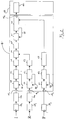
- the control and processing unit 16 is realized with a plurality of FPGA-units (Field Programmable Gate Array).
- the first analog electrical signal I enters a first analog-digital converter 30 1
- the second analog electrical signal R enters a second analog-digital converter 30 2
- the analog position signal P enters a third analog-digital converter 30 3 .
- From the first analog-digital converter 30 1 and from the second analog-digital converter 30 2 the digitized signal are fed to a first and a second delay-modules 32 and 34 respectively which are used to carry out run-time differences.
- the use of the first and second delay-module 32 an 34 is important since the first and second electric signal I and R have a processing time which is different to the position signal P. This means that the reaction time of the scanning mirror system 7 is delayed due to its inertia.
- the delag modules eliminate the possible error due to its own processing time and reaction time differences.
- the output of the first and second delay module 32 and 34 is fed to the first and second input port 16 1 and 16 2 respectively of the control and processing unit 16.
- the digital signal from the first delay-module 32 is sent to a first adder 40 followed by a first buffer 42.
- the data are sent to an address look-up-table 63 which carries out correction of the position data with respect to the scan along the x-direction.
- an address look-up-table 63 which carries out correction of the position data with respect to the scan along the x-direction.
- the calculation device 44 subtracts the data representative of the first electrical signal I from the data representative of the second electrical signal R. This enables a correction of the short term intensity fluctuations of the laser output signal.
- the data from the calculation device 44 are fed to a fourth look-up-table 45, which carries out a conversion of the data with respect to the basis e. The result of this conversion is that the data are available as the quotient of data representing the first electrical signal I and data representing the second electrical signal R.
- the data from the forth look-up table 45 are fed to a forth adder and from there to a line buffer 47 which correlates a specific digital position signal with a specific digital detection signal.
- Fig. 3 shows and ideal path 110 of the focus of the scanning beam across specimen area of interest 112.
- the dashed line represents the ideal path 110.
- the ideal path 110 comprises a plurality of linear movements 114 of the focused beam in a direction x of the specimen area 112.
- the linear movements 114 are separated by a constant line feed 116 which has a direction y, perpendicular to the linear movements 114.
- the ideal path 110 of the focus of the scanning beam would be a back and forth pattern of parallel lines in the direction x which are separated by the constant line feed 116 in the direction y.
- the line feed 116 is done by tilting the y-mirror (not shown), thereby moving the focus of the scanning beam to the next line. This next line is scanned with the x-mirror (not shown) followed by another line feed 116 and so on until the whole specimen area 112 is scanned.
- the ideal path 110 as shown in Fig. 3 can not be achieved, because of the inertia of the mirrors and the and the moving galvanometer elements.
- a real path 120 across the specimen area of interest 112 is shown in Fig. 4.
- the form of the real path is sinusoidal. According to the differences between the ideal path 110 and the actual path 120 a correction of this difference is necessary. Furthermore, it has to be considered that the velocity of the focus of the scanning beam in the direction x increases at turning points 122 compared to linear regions 124 of the sinusoidal curve.
- a real time processing unit field programmable gate array, FPGA
- FPGA field programmable gate array
- the FPGA provides also a correction in the case of an asymmetric scan path (the scan path in the x-direction differs from the scan path in the opposite direction). This requires a different correction for the scan path in the x-direction and another correction for the scan path in the opposite direction. In other words, the position signal has to be corrected with respect to the different paths of the scanning beam across the object.
Landscapes
- Physics & Mathematics (AREA)
- Chemical & Material Sciences (AREA)
- Analytical Chemistry (AREA)
- General Physics & Mathematics (AREA)
- Optics & Photonics (AREA)
- Engineering & Computer Science (AREA)
- Computer Vision & Pattern Recognition (AREA)
- General Engineering & Computer Science (AREA)
- Microscoopes, Condenser (AREA)
Abstract
Description
at least three different analog signal are generated the by confocal microscope;
- 2
- illumination system
- 4
- beam splitter.
- 6
- scanning device
- 7
- scanning mirror system
- 8
- optical system
- 10
- specimen
- 12
- first detector
- 14
- second detector
- 16
- control and processing unit
- 161
- first input port
- 162
- second input port
- 163
- third input port
- 164
- exit port
- 18
- electrical connection
- 20
- computer
- 22
- display
- 301
- first analog-digital converter
- 302
- second analog-digital converter
- 303
- third analog-digital converter
- 32
- first delay-module
- 34
- second delay-module
- 40
- first adder
- 42
- first buffer
- 43
- first look-up-table
- 44
- calculation device
- 45
- forth look-up-table
- 46
- forth adder
- 47
- line buffer
- 48
- loop1
- 50
- second adder
- 52
- second butter
- 53
- second look-up-table
- 60
- third adder
- 62
- third buffer
- 63
- address look-up-table
- 70
- loop
- 80
- loop
- 90
- loop
- 100
- computer
- 110
- ideal path
- 112
- specimen area of interest
- 114
- linear movement
- 116
- line feed
- 120
- real path
- 122
- turning point
- 124
- linear region
- I
- first electrical signal
- R
- second electrical signal
- P
- position signal
- L
- light beam
- L1
- first path
- L2
- second path
- X
- scan direction
- Y
- scan direction
Claims (14)
- A system for processing scan-signals from a confocal microscope, the system characterized in that:at least three different analog signal (I, R, P) are generated the by confocal microscope;at least three analog digital converters (301, 302, 303) are provided for receiving a different analog signal and producing respective digital signals at an early stage; anda control and processing unit (16) uses at least one programmable device for processing the digital signals in real-time.
- The system as recited in claim 1 wherein the programmable device is a field programmable gate array.
- The system as recited in claim 1 wherein the three different analog signals (I, R, P) are generated by the confocal microscope, the three different signals comprise a first electrical signal (301) which is proportional to the intensity of the light received form the a specimen (10), a second electrical signal (302) which is an illumination reference and a third electrical signal (303) which is a position signal of an actual position of a scanning light beam on the specimen (10).
- The system as recited in claim 3 wherein the control and processing unit (16) comprises a address look up table (63) to provide a correction for the position signal (P).
- The system as recited in claim 4 wherein the position signal (P) generated from a scan in the x-direction is different from a scan in the opposite direction x-direction with respect to time, and the correction of the position signal (P) is chosen with respect to the scan direction.
- The system as recited in claim 1 wherein the control and processing unit (16) comprises a calculation device (44) to correct short term intensity fluctuations, and a line buffer (47) to correlate a specific digital position signal with a specific digital detection signal.
- The system as recited in claims 1 to 6 is incorporated in a confocal microscope, wherein the confocal microscope comprising:an illumination source (2);a scanning device (6) with a scanning mirror system (7);a first detector (12) generates analog signals (I) from light reflected from the specimen (10);a second detector (14) generates analog signals (R) proportional to the intensity of the light from the illumination source (2); andan electrical connection (18) providing an analog position signal (P) generated by the scanning device, to the control and processing unit (16).
- A method for processing scan-signals from a confocal microscope, is characterized by the following steps:generating at least three different analog signals (I, P, R) by the confocal microscope wherein a first signal (I) represents light reflected from a specimen (10), a second signal (P) represents an illumination reference and a third signal (R) represents a position on the specimen (10);converting each analog signal with a separate analog digital converter (301, 302, 303) into respective digital signals;providing the digital signals to a control and processing unit (16) which uses a plurality of programmable devices for processing the digital signals in real-time;buffering the digital position signals in a line-buffer of the control and processing unit (16);correcting the first digital signal (I) for intensity fluctuations of the second digital signal (R) for generating a corrected digital detection signal; andcombining a specific digital position signal with a specific digital detection signal.
- The method as recited in claim 8 wherein the control and processing unit (16) comprises programmable devices which are field programmable gate arrays.
- The method as recited in claim 8 comprises an additional step of providing a correction for the position signal (P) with the control and processing unit (16), wherein the correction is implemented in a address look up table (63).
- The method as recited in claim 10 wherein the correction of the position signal (P) is done by providing a correction for the scan in the x-direction and a different correction for the scan in the opposite x-direction.
- The method as recited in claim 8 wherein a first look-up table (43) carries out a log conversion of the first electrical signal (I).
- The method as recited in claim 8 wherein a second look-up table (53) carries out a log conversion of the second electrical signal (R).
- The method as recited in claim 8 comprises the steps of: providing the combined digital position signal and the digital detection signal to a computer (20); and
displaying and image of the scanned specimen area.
Applications Claiming Priority (2)
| Application Number | Priority Date | Filing Date | Title |
|---|---|---|---|
| US476589 | 1999-12-31 | ||
| US09/476,589 US6423960B1 (en) | 1999-12-31 | 1999-12-31 | Method and system for processing scan-data from a confocal microscope |
Publications (3)
| Publication Number | Publication Date |
|---|---|
| EP1115021A2 true EP1115021A2 (en) | 2001-07-11 |
| EP1115021A3 EP1115021A3 (en) | 2004-10-20 |
| EP1115021B1 EP1115021B1 (en) | 2007-01-31 |
Family
ID=23892463
Family Applications (1)
| Application Number | Title | Priority Date | Filing Date |
|---|---|---|---|
| EP00126647A Expired - Lifetime EP1115021B1 (en) | 1999-12-31 | 2000-12-05 | Method and system for processing scan-data from a confocal microscope |
Country Status (3)
| Country | Link |
|---|---|
| US (1) | US6423960B1 (en) |
| EP (1) | EP1115021B1 (en) |
| DE (1) | DE60033227T2 (en) |
Cited By (10)
| Publication number | Priority date | Publication date | Assignee | Title |
|---|---|---|---|---|
| WO2005015284A1 (en) * | 2003-08-12 | 2005-02-17 | Leica Microsystems Cms Gmbh | Apparatus for the detection of photons of a light beam |
| US6859273B2 (en) | 2001-07-23 | 2005-02-22 | University Of Rochester | Method for operating a laser scanning confocal microscope system and a system thereof |
| EP1496384A3 (en) * | 2003-07-11 | 2005-03-16 | CARL ZEISS JENA GmbH | System for the detection of the illumination intensity in a laser scanning microscope |
| EP1617250A1 (en) * | 2004-07-16 | 2006-01-18 | CARL ZEISS JENA GmbH | Method for acquisition of at least one region of interest with a light scanning microscope having a linear illumination |
| EP1617267A3 (en) * | 2004-07-16 | 2006-03-15 | CARL ZEISS JENA GmbH | Method for acquisition of at least one region of interest with a light scanning microscope having a linear illumination |
| US7027221B2 (en) | 2002-04-18 | 2006-04-11 | Leica Microsystems Cms Gmbh | Autofocus method for a microscope and system for adjusting the focus for a microscope |
| WO2009021659A1 (en) * | 2007-08-16 | 2009-02-19 | Carl Zeiss Microimaging Gmbh | Microscope having internal focusing |
| EP2573613A1 (en) * | 2011-09-09 | 2013-03-27 | Sony Corporation | Information processing apparatus, information processing method, program, and information processing system |
| DE102006034905B4 (en) * | 2006-07-28 | 2015-07-30 | Carl Zeiss Microscopy Gmbh | Arrangement for signal processing at the output of a multi-channel detector |
| CN109143943A (en) * | 2018-11-06 | 2019-01-04 | 上海航天电子通讯设备研究所 | A kind of beam control device and phased array antenna |
Families Citing this family (22)
| Publication number | Priority date | Publication date | Assignee | Title |
|---|---|---|---|---|
| DE10024404A1 (en) * | 2000-05-19 | 2001-11-22 | Leica Microsystems | Confocal optical scanning microscopy produces signals influencing object and initiating measurement in accordance with given scanning locations |
| DE102004003993A1 (en) * | 2003-08-12 | 2005-03-17 | Leica Microsystems Heidelberg Gmbh | Device for detecting photons of a light beam |
| US7372985B2 (en) | 2003-08-15 | 2008-05-13 | Massachusetts Institute Of Technology | Systems and methods for volumetric tissue scanning microscopy |
| JP4677728B2 (en) * | 2004-03-22 | 2011-04-27 | 株式会社ニコン | Confocal microscope and confocal microscope system |
| US9080894B2 (en) | 2004-10-20 | 2015-07-14 | Electro Industries/Gauge Tech | Intelligent electronic device for receiving and sending data at high speeds over a network |
| US7304586B2 (en) | 2004-10-20 | 2007-12-04 | Electro Industries / Gauge Tech | On-line web accessed energy meter |
| US7747733B2 (en) | 2004-10-25 | 2010-06-29 | Electro Industries/Gauge Tech | Power meter having multiple ethernet ports |
| US7916060B2 (en) * | 2005-01-27 | 2011-03-29 | Electro Industries/Gauge Tech. | Intelligent electronic device having circuitry for noise reduction for analog-to-digital converters |
| US8620608B2 (en) | 2005-01-27 | 2013-12-31 | Electro Industries/Gauge Tech | Intelligent electronic device and method thereof |
| US8190381B2 (en) | 2005-01-27 | 2012-05-29 | Electro Industries/Gauge Tech | Intelligent electronic device with enhanced power quality monitoring and communications capabilities |
| US8160824B2 (en) | 2005-01-27 | 2012-04-17 | Electro Industries/Gauge Tech | Intelligent electronic device with enhanced power quality monitoring and communication capabilities |
| US8930153B2 (en) | 2005-01-27 | 2015-01-06 | Electro Industries/Gauge Tech | Metering device with control functionality and method thereof |
| EP2703871A3 (en) | 2005-05-25 | 2014-09-03 | Massachusetts Institute Of Technology | Multifocal scanning microscopy systems and methods |
| US8587949B2 (en) | 2007-03-27 | 2013-11-19 | Electro Industries/Gauge Tech | Electronic meter having user-interface and central processing functionality on a single printed circuit board |
| US10845399B2 (en) | 2007-04-03 | 2020-11-24 | Electro Industries/Gaugetech | System and method for performing data transfers in an intelligent electronic device |
| US9989618B2 (en) | 2007-04-03 | 2018-06-05 | Electro Industries/Gaugetech | Intelligent electronic device with constant calibration capabilities for high accuracy measurements |
| US20130275066A1 (en) | 2007-04-03 | 2013-10-17 | Electro Industries/Gaugetech | Digital power metering system |
| US8797202B2 (en) | 2008-03-13 | 2014-08-05 | Electro Industries/Gauge Tech | Intelligent electronic device having circuitry for highly accurate voltage sensing |
| US12061218B2 (en) | 2008-03-13 | 2024-08-13 | Ei Electronics Llc | System and method for multi-rate concurrent waveform capture and storage for power quality metering |
| WO2016145366A1 (en) | 2015-03-11 | 2016-09-15 | Timothy Ragan | System and methods for serial staining and imaging |
| WO2018094290A1 (en) | 2016-11-18 | 2018-05-24 | Tissuevision, Inc. | Automated tissue section capture, indexing and storage system and methods |
| CN109557652B (en) * | 2018-11-30 | 2024-04-05 | 南京博视医疗科技有限公司 | Light source modulation method for confocal scanning microscope |
Family Cites Families (9)
| Publication number | Priority date | Publication date | Assignee | Title |
|---|---|---|---|---|
| NL8701716A (en) * | 1987-07-21 | 1989-02-16 | Philips Nv | SCANNING OPTICAL MICROSCOPE. |
| US5296703A (en) * | 1992-04-01 | 1994-03-22 | The Regents Of The University Of California | Scanning confocal microscope using fluorescence detection |
| US5589936A (en) * | 1992-09-14 | 1996-12-31 | Nikon Corporation | Optical measuring apparatus for measuring physichemical properties |
| US5283433A (en) * | 1992-10-05 | 1994-02-01 | The Regents Of The University Of California | Scanning confocal microscope providing a continuous display |
| JP3343276B2 (en) * | 1993-04-15 | 2002-11-11 | 興和株式会社 | Laser scanning optical microscope |
| US5804813A (en) | 1996-06-06 | 1998-09-08 | National Science Council Of Republic Of China | Differential confocal microscopy |
| DE19702753C2 (en) * | 1997-01-27 | 2003-04-10 | Zeiss Carl Jena Gmbh | Laser Scanning Microscope |
| US6248988B1 (en) * | 1998-05-05 | 2001-06-19 | Kla-Tencor Corporation | Conventional and confocal multi-spot scanning optical microscope |
| US6303916B1 (en) * | 1998-12-24 | 2001-10-16 | Mitutoyo Corporation | Systems and methods for generating reproducible illumination |
-
1999
- 1999-12-31 US US09/476,589 patent/US6423960B1/en not_active Expired - Lifetime
-
2000
- 2000-12-05 DE DE60033227T patent/DE60033227T2/en not_active Expired - Lifetime
- 2000-12-05 EP EP00126647A patent/EP1115021B1/en not_active Expired - Lifetime
Cited By (17)
| Publication number | Priority date | Publication date | Assignee | Title |
|---|---|---|---|---|
| US6859273B2 (en) | 2001-07-23 | 2005-02-22 | University Of Rochester | Method for operating a laser scanning confocal microscope system and a system thereof |
| US6956647B2 (en) | 2001-07-23 | 2005-10-18 | University Of Rochester | Method for operating a laser scanning confocal microscope system and a system thereof |
| US7027221B2 (en) | 2002-04-18 | 2006-04-11 | Leica Microsystems Cms Gmbh | Autofocus method for a microscope and system for adjusting the focus for a microscope |
| EP1496384A3 (en) * | 2003-07-11 | 2005-03-16 | CARL ZEISS JENA GmbH | System for the detection of the illumination intensity in a laser scanning microscope |
| US7498561B2 (en) | 2003-07-11 | 2009-03-03 | Carl Zeiss Microimaging Gmbh | Arrangement for the detection of illumination radiation in a laser scanning microscope |
| EP1780572A1 (en) * | 2003-07-11 | 2007-05-02 | CARL ZEISS JENA GmbH | System for the detection of the illumination intensity in a laser scanning microscope |
| US7259366B2 (en) | 2003-08-12 | 2007-08-21 | Leica Microsystems Cms Gmbh | Apparatus for the detection of photons of a light beam having a three-dimensional array of detectors |
| WO2005015284A1 (en) * | 2003-08-12 | 2005-02-17 | Leica Microsystems Cms Gmbh | Apparatus for the detection of photons of a light beam |
| EP1617250A1 (en) * | 2004-07-16 | 2006-01-18 | CARL ZEISS JENA GmbH | Method for acquisition of at least one region of interest with a light scanning microscope having a linear illumination |
| US7459698B2 (en) | 2004-07-16 | 2008-12-02 | Carl Zeiss Microimaging Gmbh | Process for the observation of at least one sample region with a light raster microscope |
| EP1617267A3 (en) * | 2004-07-16 | 2006-03-15 | CARL ZEISS JENA GmbH | Method for acquisition of at least one region of interest with a light scanning microscope having a linear illumination |
| US7649683B2 (en) | 2004-07-16 | 2010-01-19 | Carl Zeiss Microimaging Gmbh | Process for the observation of at least one sample region with a light raster microscope with linear sampling |
| DE102006034905B4 (en) * | 2006-07-28 | 2015-07-30 | Carl Zeiss Microscopy Gmbh | Arrangement for signal processing at the output of a multi-channel detector |
| WO2009021659A1 (en) * | 2007-08-16 | 2009-02-19 | Carl Zeiss Microimaging Gmbh | Microscope having internal focusing |
| US8553324B2 (en) | 2007-08-16 | 2013-10-08 | Carl Zeiss Microscopy Gmbh | Microscope having internal focusing |
| EP2573613A1 (en) * | 2011-09-09 | 2013-03-27 | Sony Corporation | Information processing apparatus, information processing method, program, and information processing system |
| CN109143943A (en) * | 2018-11-06 | 2019-01-04 | 上海航天电子通讯设备研究所 | A kind of beam control device and phased array antenna |
Also Published As
| Publication number | Publication date |
|---|---|
| DE60033227T2 (en) | 2007-11-15 |
| EP1115021B1 (en) | 2007-01-31 |
| US6423960B1 (en) | 2002-07-23 |
| EP1115021A3 (en) | 2004-10-20 |
| DE60033227D1 (en) | 2007-03-22 |
Similar Documents
| Publication | Publication Date | Title |
|---|---|---|
| EP1115021B1 (en) | Method and system for processing scan-data from a confocal microscope | |
| EP0834758B1 (en) | Continuous volume imaging system for scanning microscopy | |
| EP0284136B1 (en) | Confocal laser scanning microscope | |
| US7576307B2 (en) | Microscope with dual image sensors for rapid autofocusing | |
| US4893008A (en) | Scanning optical microscope | |
| US4845552A (en) | Quantitative light microscope using a solid state detector in the primary image plane | |
| US7399647B2 (en) | Multi beam scanning with bright/dark field imaging | |
| US6236454B1 (en) | Multiple beam scanner for an inspection system | |
| US6444971B1 (en) | Method and system for compensating intensity fluctuations of an illumination system in a confocal microscope | |
| EP0716327A1 (en) | Laser scanning microscope | |
| EP0300571B1 (en) | Scanning optical microscope | |
| JPH0117523B2 (en) | ||
| HUP0401802A2 (en) | Focusing method object carriers on fast-moving digitalization and object carrier moving mechanics, focusing optic, optical distance-measuring instrument | |
| JPH0666241B2 (en) | Position detection method | |
| US12345661B2 (en) | Defect inspection apparatus and defect inspection method | |
| JPH11211439A (en) | Surface profile measuring device | |
| JPH09126739A (en) | 3D shape measuring device | |
| JPH11231223A (en) | Scanning optical microscope | |
| US6172785B1 (en) | Light-scanning device | |
| WO2003012525A1 (en) | Optical system and method for producing focused and defocused images | |
| JP3708277B2 (en) | Scanning optical measuring device | |
| JP2633718B2 (en) | Shape recognition device | |
| JP2003057553A (en) | Confocal scanning microscope | |
| KR100519266B1 (en) | Confocal microscope | |
| US20040119001A1 (en) | Eliminating coherence effects in bright-field laser imaging |
Legal Events
| Date | Code | Title | Description |
|---|---|---|---|
| PUAI | Public reference made under article 153(3) epc to a published international application that has entered the european phase |
Free format text: ORIGINAL CODE: 0009012 |
|
| AK | Designated contracting states |
Kind code of ref document: A2 Designated state(s): AT BE CH CY DE DK ES FI FR GB GR IE IT LI LU MC NL PT SE TR |
|
| AX | Request for extension of the european patent |
Free format text: AL;LT;LV;MK;RO;SI |
|
| PUAL | Search report despatched |
Free format text: ORIGINAL CODE: 0009013 |
|
| AK | Designated contracting states |
Kind code of ref document: A3 Designated state(s): AT BE CH CY DE DK ES FI FR GB GR IE IT LI LU MC NL PT SE TR |
|
| AX | Request for extension of the european patent |
Extension state: AL LT LV MK RO SI |
|
| 17P | Request for examination filed |
Effective date: 20050323 |
|
| 17Q | First examination report despatched |
Effective date: 20050427 |
|
| AKX | Designation fees paid |
Designated state(s): DE GB |
|
| RAP1 | Party data changed (applicant data changed or rights of an application transferred) |
Owner name: LEICA MICROSYSTEMS CMS GMBH |
|
| GRAP | Despatch of communication of intention to grant a patent |
Free format text: ORIGINAL CODE: EPIDOSNIGR1 |
|
| RTI1 | Title (correction) |
Free format text: METHOD AND SYSTEM FOR PROCESSING SCAN-DATA FROM A CONFOCAL MICROSCOPE |
|
| GRAS | Grant fee paid |
Free format text: ORIGINAL CODE: EPIDOSNIGR3 |
|
| GRAA | (expected) grant |
Free format text: ORIGINAL CODE: 0009210 |
|
| AK | Designated contracting states |
Kind code of ref document: B1 Designated state(s): DE GB |
|
| REG | Reference to a national code |
Ref country code: GB Ref legal event code: FG4D |
|
| REF | Corresponds to: |
Ref document number: 60033227 Country of ref document: DE Date of ref document: 20070322 Kind code of ref document: P |
|
| PLBE | No opposition filed within time limit |
Free format text: ORIGINAL CODE: 0009261 |
|
| STAA | Information on the status of an ep patent application or granted ep patent |
Free format text: STATUS: NO OPPOSITION FILED WITHIN TIME LIMIT |
|
| 26N | No opposition filed |
Effective date: 20071101 |
|
| PGFP | Annual fee paid to national office [announced via postgrant information from national office to epo] |
Ref country code: GB Payment date: 20151221 Year of fee payment: 16 Ref country code: DE Payment date: 20151210 Year of fee payment: 16 |
|
| REG | Reference to a national code |
Ref country code: DE Ref legal event code: R119 Ref document number: 60033227 Country of ref document: DE |
|
| GBPC | Gb: european patent ceased through non-payment of renewal fee |
Effective date: 20161205 |
|
| PG25 | Lapsed in a contracting state [announced via postgrant information from national office to epo] |
Ref country code: DE Free format text: LAPSE BECAUSE OF NON-PAYMENT OF DUE FEES Effective date: 20170701 Ref country code: GB Free format text: LAPSE BECAUSE OF NON-PAYMENT OF DUE FEES Effective date: 20161205 |