EP1114457B1 - Method for producing integrated circuits - Google Patents
Method for producing integrated circuits Download PDFInfo
- Publication number
- EP1114457B1 EP1114457B1 EP99952270A EP99952270A EP1114457B1 EP 1114457 B1 EP1114457 B1 EP 1114457B1 EP 99952270 A EP99952270 A EP 99952270A EP 99952270 A EP99952270 A EP 99952270A EP 1114457 B1 EP1114457 B1 EP 1114457B1
- Authority
- EP
- European Patent Office
- Prior art keywords
- semiconductor wafer
- intermediate layer
- conductive
- opening
- applying
- Prior art date
- Legal status (The legal status is an assumption and is not a legal conclusion. Google has not performed a legal analysis and makes no representation as to the accuracy of the status listed.)
- Expired - Lifetime
Links
Images

Classifications
-
- H—ELECTRICITY
- H01—ELECTRIC ELEMENTS
- H01L—SEMICONDUCTOR DEVICES NOT COVERED BY CLASS H10
- H01L24/00—Arrangements for connecting or disconnecting semiconductor or solid-state bodies; Methods or apparatus related thereto
- H01L24/01—Means for bonding being attached to, or being formed on, the surface to be connected, e.g. chip-to-package, die-attach, "first-level" interconnects; Manufacturing methods related thereto
- H01L24/10—Bump connectors ; Manufacturing methods related thereto
- H01L24/12—Structure, shape, material or disposition of the bump connectors prior to the connecting process
-
- H—ELECTRICITY
- H01—ELECTRIC ELEMENTS
- H01L—SEMICONDUCTOR DEVICES NOT COVERED BY CLASS H10
- H01L23/00—Details of semiconductor or other solid state devices
- H01L23/48—Arrangements for conducting electric current to or from the solid state body in operation, e.g. leads, terminal arrangements ; Selection of materials therefor
- H01L23/488—Arrangements for conducting electric current to or from the solid state body in operation, e.g. leads, terminal arrangements ; Selection of materials therefor consisting of soldered or bonded constructions
- H01L23/498—Leads, i.e. metallisations or lead-frames on insulating substrates, e.g. chip carriers
- H01L23/49811—Additional leads joined to the metallisation on the insulating substrate, e.g. pins, bumps, wires, flat leads
- H01L23/49816—Spherical bumps on the substrate for external connection, e.g. ball grid arrays [BGA]
-
- H—ELECTRICITY
- H01—ELECTRIC ELEMENTS
- H01L—SEMICONDUCTOR DEVICES NOT COVERED BY CLASS H10
- H01L23/00—Details of semiconductor or other solid state devices
- H01L23/48—Arrangements for conducting electric current to or from the solid state body in operation, e.g. leads, terminal arrangements ; Selection of materials therefor
- H01L23/488—Arrangements for conducting electric current to or from the solid state body in operation, e.g. leads, terminal arrangements ; Selection of materials therefor consisting of soldered or bonded constructions
- H01L23/498—Leads, i.e. metallisations or lead-frames on insulating substrates, e.g. chip carriers
- H01L23/4985—Flexible insulating substrates
-
- H—ELECTRICITY
- H01—ELECTRIC ELEMENTS
- H01L—SEMICONDUCTOR DEVICES NOT COVERED BY CLASS H10
- H01L24/00—Arrangements for connecting or disconnecting semiconductor or solid-state bodies; Methods or apparatus related thereto
- H01L24/01—Means for bonding being attached to, or being formed on, the surface to be connected, e.g. chip-to-package, die-attach, "first-level" interconnects; Manufacturing methods related thereto
- H01L24/10—Bump connectors ; Manufacturing methods related thereto
- H01L24/11—Manufacturing methods
-
- H—ELECTRICITY
- H01—ELECTRIC ELEMENTS
- H01L—SEMICONDUCTOR DEVICES NOT COVERED BY CLASS H10
- H01L24/00—Arrangements for connecting or disconnecting semiconductor or solid-state bodies; Methods or apparatus related thereto
- H01L24/01—Means for bonding being attached to, or being formed on, the surface to be connected, e.g. chip-to-package, die-attach, "first-level" interconnects; Manufacturing methods related thereto
- H01L24/26—Layer connectors, e.g. plate connectors, solder or adhesive layers; Manufacturing methods related thereto
- H01L24/28—Structure, shape, material or disposition of the layer connectors prior to the connecting process
- H01L24/29—Structure, shape, material or disposition of the layer connectors prior to the connecting process of an individual layer connector
-
- H—ELECTRICITY
- H01—ELECTRIC ELEMENTS
- H01L—SEMICONDUCTOR DEVICES NOT COVERED BY CLASS H10
- H01L24/00—Arrangements for connecting or disconnecting semiconductor or solid-state bodies; Methods or apparatus related thereto
- H01L24/80—Methods for connecting semiconductor or other solid state bodies using means for bonding being attached to, or being formed on, the surface to be connected
- H01L24/83—Methods for connecting semiconductor or other solid state bodies using means for bonding being attached to, or being formed on, the surface to be connected using a layer connector
-
- H—ELECTRICITY
- H01—ELECTRIC ELEMENTS
- H01L—SEMICONDUCTOR DEVICES NOT COVERED BY CLASS H10
- H01L2224/00—Indexing scheme for arrangements for connecting or disconnecting semiconductor or solid-state bodies and methods related thereto as covered by H01L24/00
- H01L2224/01—Means for bonding being attached to, or being formed on, the surface to be connected, e.g. chip-to-package, die-attach, "first-level" interconnects; Manufacturing methods related thereto
- H01L2224/02—Bonding areas; Manufacturing methods related thereto
- H01L2224/023—Redistribution layers [RDL] for bonding areas
-
- H—ELECTRICITY
- H01—ELECTRIC ELEMENTS
- H01L—SEMICONDUCTOR DEVICES NOT COVERED BY CLASS H10
- H01L2224/00—Indexing scheme for arrangements for connecting or disconnecting semiconductor or solid-state bodies and methods related thereto as covered by H01L24/00
- H01L2224/01—Means for bonding being attached to, or being formed on, the surface to be connected, e.g. chip-to-package, die-attach, "first-level" interconnects; Manufacturing methods related thereto
- H01L2224/10—Bump connectors; Manufacturing methods related thereto
- H01L2224/12—Structure, shape, material or disposition of the bump connectors prior to the connecting process
- H01L2224/13—Structure, shape, material or disposition of the bump connectors prior to the connecting process of an individual bump connector
- H01L2224/13001—Core members of the bump connector
- H01L2224/13099—Material
-
- H—ELECTRICITY
- H01—ELECTRIC ELEMENTS
- H01L—SEMICONDUCTOR DEVICES NOT COVERED BY CLASS H10
- H01L2224/00—Indexing scheme for arrangements for connecting or disconnecting semiconductor or solid-state bodies and methods related thereto as covered by H01L24/00
- H01L2224/01—Means for bonding being attached to, or being formed on, the surface to be connected, e.g. chip-to-package, die-attach, "first-level" interconnects; Manufacturing methods related thereto
- H01L2224/26—Layer connectors, e.g. plate connectors, solder or adhesive layers; Manufacturing methods related thereto
- H01L2224/28—Structure, shape, material or disposition of the layer connectors prior to the connecting process
- H01L2224/29—Structure, shape, material or disposition of the layer connectors prior to the connecting process of an individual layer connector
- H01L2224/29001—Core members of the layer connector
- H01L2224/29099—Material
- H01L2224/291—Material with a principal constituent of the material being a metal or a metalloid, e.g. boron [B], silicon [Si], germanium [Ge], arsenic [As], antimony [Sb], tellurium [Te] and polonium [Po], and alloys thereof
- H01L2224/29101—Material with a principal constituent of the material being a metal or a metalloid, e.g. boron [B], silicon [Si], germanium [Ge], arsenic [As], antimony [Sb], tellurium [Te] and polonium [Po], and alloys thereof the principal constituent melting at a temperature of less than 400°C
-
- H—ELECTRICITY
- H01—ELECTRIC ELEMENTS
- H01L—SEMICONDUCTOR DEVICES NOT COVERED BY CLASS H10
- H01L2224/00—Indexing scheme for arrangements for connecting or disconnecting semiconductor or solid-state bodies and methods related thereto as covered by H01L24/00
- H01L2224/01—Means for bonding being attached to, or being formed on, the surface to be connected, e.g. chip-to-package, die-attach, "first-level" interconnects; Manufacturing methods related thereto
- H01L2224/26—Layer connectors, e.g. plate connectors, solder or adhesive layers; Manufacturing methods related thereto
- H01L2224/28—Structure, shape, material or disposition of the layer connectors prior to the connecting process
- H01L2224/29—Structure, shape, material or disposition of the layer connectors prior to the connecting process of an individual layer connector
- H01L2224/29001—Core members of the layer connector
- H01L2224/29099—Material
- H01L2224/29198—Material with a principal constituent of the material being a combination of two or more materials in the form of a matrix with a filler, i.e. being a hybrid material, e.g. segmented structures, foams
- H01L2224/29199—Material of the matrix
- H01L2224/2929—Material of the matrix with a principal constituent of the material being a polymer, e.g. polyester, phenolic based polymer, epoxy
-
- H—ELECTRICITY
- H01—ELECTRIC ELEMENTS
- H01L—SEMICONDUCTOR DEVICES NOT COVERED BY CLASS H10
- H01L2224/00—Indexing scheme for arrangements for connecting or disconnecting semiconductor or solid-state bodies and methods related thereto as covered by H01L24/00
- H01L2224/01—Means for bonding being attached to, or being formed on, the surface to be connected, e.g. chip-to-package, die-attach, "first-level" interconnects; Manufacturing methods related thereto
- H01L2224/26—Layer connectors, e.g. plate connectors, solder or adhesive layers; Manufacturing methods related thereto
- H01L2224/28—Structure, shape, material or disposition of the layer connectors prior to the connecting process
- H01L2224/29—Structure, shape, material or disposition of the layer connectors prior to the connecting process of an individual layer connector
- H01L2224/29001—Core members of the layer connector
- H01L2224/29099—Material
- H01L2224/29198—Material with a principal constituent of the material being a combination of two or more materials in the form of a matrix with a filler, i.e. being a hybrid material, e.g. segmented structures, foams
- H01L2224/29298—Fillers
- H01L2224/29299—Base material
- H01L2224/293—Base material with a principal constituent of the material being a metal or a metalloid, e.g. boron [B], silicon [Si], germanium [Ge], arsenic [As], antimony [Sb], tellurium [Te] and polonium [Po], and alloys thereof
-
- H—ELECTRICITY
- H01—ELECTRIC ELEMENTS
- H01L—SEMICONDUCTOR DEVICES NOT COVERED BY CLASS H10
- H01L2224/00—Indexing scheme for arrangements for connecting or disconnecting semiconductor or solid-state bodies and methods related thereto as covered by H01L24/00
- H01L2224/80—Methods for connecting semiconductor or other solid state bodies using means for bonding being attached to, or being formed on, the surface to be connected
- H01L2224/83—Methods for connecting semiconductor or other solid state bodies using means for bonding being attached to, or being formed on, the surface to be connected using a layer connector
- H01L2224/8319—Arrangement of the layer connectors prior to mounting
-
- H—ELECTRICITY
- H01—ELECTRIC ELEMENTS
- H01L—SEMICONDUCTOR DEVICES NOT COVERED BY CLASS H10
- H01L2224/00—Indexing scheme for arrangements for connecting or disconnecting semiconductor or solid-state bodies and methods related thereto as covered by H01L24/00
- H01L2224/80—Methods for connecting semiconductor or other solid state bodies using means for bonding being attached to, or being formed on, the surface to be connected
- H01L2224/83—Methods for connecting semiconductor or other solid state bodies using means for bonding being attached to, or being formed on, the surface to be connected using a layer connector
- H01L2224/838—Bonding techniques
-
- H—ELECTRICITY
- H01—ELECTRIC ELEMENTS
- H01L—SEMICONDUCTOR DEVICES NOT COVERED BY CLASS H10
- H01L2924/00—Indexing scheme for arrangements or methods for connecting or disconnecting semiconductor or solid-state bodies as covered by H01L24/00
- H01L2924/0001—Technical content checked by a classifier
- H01L2924/00013—Fully indexed content
-
- H—ELECTRICITY
- H01—ELECTRIC ELEMENTS
- H01L—SEMICONDUCTOR DEVICES NOT COVERED BY CLASS H10
- H01L2924/00—Indexing scheme for arrangements or methods for connecting or disconnecting semiconductor or solid-state bodies as covered by H01L24/00
- H01L2924/0001—Technical content checked by a classifier
- H01L2924/00014—Technical content checked by a classifier the subject-matter covered by the group, the symbol of which is combined with the symbol of this group, being disclosed without further technical details
-
- H—ELECTRICITY
- H01—ELECTRIC ELEMENTS
- H01L—SEMICONDUCTOR DEVICES NOT COVERED BY CLASS H10
- H01L2924/00—Indexing scheme for arrangements or methods for connecting or disconnecting semiconductor or solid-state bodies as covered by H01L24/00
- H01L2924/01—Chemical elements
- H01L2924/01005—Boron [B]
-
- H—ELECTRICITY
- H01—ELECTRIC ELEMENTS
- H01L—SEMICONDUCTOR DEVICES NOT COVERED BY CLASS H10
- H01L2924/00—Indexing scheme for arrangements or methods for connecting or disconnecting semiconductor or solid-state bodies as covered by H01L24/00
- H01L2924/01—Chemical elements
- H01L2924/01006—Carbon [C]
-
- H—ELECTRICITY
- H01—ELECTRIC ELEMENTS
- H01L—SEMICONDUCTOR DEVICES NOT COVERED BY CLASS H10
- H01L2924/00—Indexing scheme for arrangements or methods for connecting or disconnecting semiconductor or solid-state bodies as covered by H01L24/00
- H01L2924/01—Chemical elements
- H01L2924/01019—Potassium [K]
-
- H—ELECTRICITY
- H01—ELECTRIC ELEMENTS
- H01L—SEMICONDUCTOR DEVICES NOT COVERED BY CLASS H10
- H01L2924/00—Indexing scheme for arrangements or methods for connecting or disconnecting semiconductor or solid-state bodies as covered by H01L24/00
- H01L2924/01—Chemical elements
- H01L2924/01029—Copper [Cu]
-
- H—ELECTRICITY
- H01—ELECTRIC ELEMENTS
- H01L—SEMICONDUCTOR DEVICES NOT COVERED BY CLASS H10
- H01L2924/00—Indexing scheme for arrangements or methods for connecting or disconnecting semiconductor or solid-state bodies as covered by H01L24/00
- H01L2924/01—Chemical elements
- H01L2924/0105—Tin [Sn]
-
- H—ELECTRICITY
- H01—ELECTRIC ELEMENTS
- H01L—SEMICONDUCTOR DEVICES NOT COVERED BY CLASS H10
- H01L2924/00—Indexing scheme for arrangements or methods for connecting or disconnecting semiconductor or solid-state bodies as covered by H01L24/00
- H01L2924/01—Chemical elements
- H01L2924/01079—Gold [Au]
-
- H—ELECTRICITY
- H01—ELECTRIC ELEMENTS
- H01L—SEMICONDUCTOR DEVICES NOT COVERED BY CLASS H10
- H01L2924/00—Indexing scheme for arrangements or methods for connecting or disconnecting semiconductor or solid-state bodies as covered by H01L24/00
- H01L2924/01—Chemical elements
- H01L2924/01082—Lead [Pb]
-
- H—ELECTRICITY
- H01—ELECTRIC ELEMENTS
- H01L—SEMICONDUCTOR DEVICES NOT COVERED BY CLASS H10
- H01L2924/00—Indexing scheme for arrangements or methods for connecting or disconnecting semiconductor or solid-state bodies as covered by H01L24/00
- H01L2924/013—Alloys
- H01L2924/014—Solder alloys
-
- H—ELECTRICITY
- H01—ELECTRIC ELEMENTS
- H01L—SEMICONDUCTOR DEVICES NOT COVERED BY CLASS H10
- H01L2924/00—Indexing scheme for arrangements or methods for connecting or disconnecting semiconductor or solid-state bodies as covered by H01L24/00
- H01L2924/06—Polymers
- H01L2924/078—Adhesive characteristics other than chemical
- H01L2924/0781—Adhesive characteristics other than chemical being an ohmic electrical conductor
- H01L2924/07811—Extrinsic, i.e. with electrical conductive fillers
-
- H—ELECTRICITY
- H01—ELECTRIC ELEMENTS
- H01L—SEMICONDUCTOR DEVICES NOT COVERED BY CLASS H10
- H01L2924/00—Indexing scheme for arrangements or methods for connecting or disconnecting semiconductor or solid-state bodies as covered by H01L24/00
- H01L2924/10—Details of semiconductor or other solid state devices to be connected
- H01L2924/11—Device type
- H01L2924/12—Passive devices, e.g. 2 terminal devices
- H01L2924/1204—Optical Diode
- H01L2924/12042—LASER
-
- H—ELECTRICITY
- H01—ELECTRIC ELEMENTS
- H01L—SEMICONDUCTOR DEVICES NOT COVERED BY CLASS H10
- H01L2924/00—Indexing scheme for arrangements or methods for connecting or disconnecting semiconductor or solid-state bodies as covered by H01L24/00
- H01L2924/10—Details of semiconductor or other solid state devices to be connected
- H01L2924/11—Device type
- H01L2924/14—Integrated circuits
Definitions
- the invention relates to a method for the production of integrated circuits.
- the prior art discloses manufacturing methods for producing integrated circuits, in particular chip-size packages of semiconductor wafers, in which circuit structures for a plurality of integrated circuits are produced in a first step on an active side of a semiconductor wafer. Thereafter, the integrated circuits are diced into so-called chips by sawing the semiconductor wafer into individual pieces at the edge regions of the integrated circuits. The chips are each contacted on so-called interposer, which can be rigid or flexible. It is also conceivable to contact a chip on a so-called leadframe. The contacting can be carried out with different bonding methods, for example with a wire bonding method, with a flip-chip bonding method or with a TAB bonding method.
- EP 0 734 059 A2 EP 0 786 808 A1 and EP 0 704 895 A2
- Methods for producing terminal contacts on semiconductor circuits are described, in which the upper side of a wafer is provided with a passivation and a conductive layer arranged above it is patterned and provided with plated-through holes to connection pads of a circuit.
- the inventive method ensures a simple production of integrated circuits.
- a relatively thick organic dielectric layer is provided for strain compensation.
- the final conductor structure with strong conductor cross-sections is only generated at the wafer level of the semiconductor wafer.
- the basic principle is based on laminating a copper foil on the semiconductor wafer, contacting the copper foil with the chip connections or the connecting contacts of the integrated circuits and only then realizing the rewiring in photo- and etching technology.
- solder balls and the separation of the semiconductor wafer can be done in single packages, for example by sawing.
- a suitable Schmidtschtechnik done on the passive chip backside In general, to achieve a particularly flat surface of a semiconductor chip together with the lamination of the Copper foil a suitable Schmidtschtechnik done on the passive chip backside.
- the step of applying the intermediate layer to at least one electrically conductive film foil is carried out before the step of applying the intermediate layer to the active side of the semiconductor wafer. From this embodiment of the method according to the invention go out the variants in which the intermediate layer is finished together with the conductive foil prior to application to the semiconductor wafer. In these embodiments of the method according to the invention is particularly advantageous that manufacturing steps that are performed on the intermediate layer and on the conductor foil, not affect the integrated circuits on the semiconductor wafer.
- the step of introducing at least one through opening into the intermediate layer may be provided, wherein the through opening is formed to extend from an underside of the conductive foil to the underside of the intermediate layer , Then, the conductive foil can be contacted through the through hole.
- the introduction of the passage opening is preferably carried out by a laser process, which can be achieved by accurate passage openings.
- conductive filler and bonding material can be introduced into the through-hole, in particular by a galvanic deposition process.
- a particularly cost-effective and reliable production of a semiconductor wafer is achieved according to the invention.
- the step of heating the solder material may be provided in the through hole, after the application of the intermediate layer on the active side of the semiconductor wafer.
- the solder material is heated in the passage opening, the solder material is melted and forms a conductive connection with the contact points provided on the semiconductor wafer.
- Such heating is preferably carried out selectively on the conductive foil in the region of the passage opening, so that the effect of heat on the semiconductor wafer is particularly low.
- conductive adhesive can be introduced as a conductive filling and bonding material in the through hole and in particular by a doctor blade method.
- the provision of conductive adhesive in the through holes favors mass production of the semiconductor wafer.
- the step of curing the conductive adhesive in the through holes may be provided, such that the conductive adhesive forms a conductive connection with both the conductive foil and contact points provided on the semiconductor wafer .
- a particularly favorable connection between the semiconductor wafer, the intermediate layer and the conductor foil results when the step of applying the intermediate layer to the active side of the semiconductor wafer is carried out with a lamination process, in particular using pressure and heat.
- step of solder stop masking of ball landing surfaces and the step of solder ball production is performed on predetermined locations of the conductive foil, which facilitating subsequent contacting of the integrated circuits provided on the semiconductor wafer.
- a semiconductor wafer produced according to the invention is characterized by an active side with circuit structures, wherein at least one electrically insulating intermediate layer and at least one electrically conductive conductor foil with conductor paths are provided on the active side.
- conductive filling and connecting material is provided between contact points on the semiconductor wafer and regions of the conductor foil.
- the finished semiconductor wafer is sawn into individual integrated circuits. This happens with very fast running cutting discs, which are equipped with diamond particles.
- the diamond particles are very thin and clamped in a mandrel so that they have little overhang.
- a sheet is numerically controlled and driven exactly clocked in the grid spacing of the integrated circuits on the semiconductor wafer, so that the integrated circuits are separated.
- the semiconductor wafer is adhered to a foil so that the integrated circuits remain in order during the sawing process. This film is mitangesägtes in sawing the semiconductor wafer.
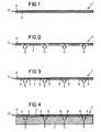
- FIGS. 1-7 illustrate the production of a semiconductor wafer by means of a cross section through its layers for a first embodiment.
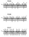
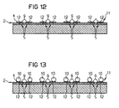
- FIGS. 8-13 illustrate the production of a semiconductor wafer by means of a cross section through its layers for a second embodiment.
- FIG. 1 shows a cross section through a printed circuit board 2, which is divided into an electrically insulating intermediate layer 3 and in a plane on the electrical intermediate layer 3 applied and electrically conductive copper cladding 4.
- the printed circuit board 2 is in the ground state, that is, as a copper-clad B-stage material or as an adhesive-coated carrier material.
- FIG. 2 illustrates the first manufacturing step for the semiconductor wafer 1.
- 2 through holes 5 are introduced into the intermediate layer 3 of the circuit board, which extend from the Kupferkaschtechnik 4 to the bottom of the intermediate layer 3.
- a laser method is preferably used.
- FIG. 3 illustrates a further manufacturing step for producing the semiconductor wafer 1.
- solder material 6 is deposited in the form of tin galvanically in the through holes 5, wherein the solder material 6 rests against the underside of the copper cladding 4.
- FIG. 4 illustrates another manufacturing step for producing the semiconductor wafer 1.
- the circuit board 2 is made FIG. 3 on a semiconductor wafer 7 applied, which has integrated circuits on its upper side.
- the connection of the printed circuit board 2 to the semiconductor wafer 7 is produced by lamination.
- the printed circuit board 2 is thereby laminated onto the semiconductor wafer 7 in such a way that the through-holes 5 come to rest precisely on Ni / Au bumps of integrated circuits on the semiconductor wafer 7 which are not shown in this view.
- FIG. 5 illustrates another manufacturing step in the production of the semiconductor wafer 1.
- Puniform heating of the top of the circuit board 2 in areas around through holes 5 around the solder material 6 is melted by means of laser beams 8, so that it intimately connected to the wettable terminals, not shown in this view, eg Ni / Au humps and with corresponding Forms of copper lamination enters and produces an electrically conductive connection between the copper cladding 4 and contact areas of the integrated circuits on the semiconductor wafer 7.
- FIG. 6 shows a further step in the production of the semiconductor wafer 1.
- conductor tracks 9 are formed in the copper cladding 4 with the aid of a photolithographic technique and with the aid of an etching technique, which allow an optional contacting of the passage openings 5.
- FIG. 7 illustrates a further manufacturing step of the semiconductor wafer 1.
- the conductor tracks 9 are provided with a solder stop mask not shown in this view, whereupon so-called balls 10 are generated on the tracks 9.
- the semiconductor wafer 1 is then sawn into so-called individual chips.
- FIGS. 8-13 illustrate the production of another semiconductor wafer 11 by means of several cross sections.
- the manufacture of the semiconductor wafer 11 essentially corresponds to the production of the semiconductor wafer 1.
- the same parts are therefore given the same reference numerals.
- All other manufacturing steps for manufacturing the semiconductor wafer 11 substantially coincide with the manufacturing steps for the semiconductor wafer.
Landscapes
- Engineering & Computer Science (AREA)
- Computer Hardware Design (AREA)
- Microelectronics & Electronic Packaging (AREA)
- Power Engineering (AREA)
- Physics & Mathematics (AREA)
- Condensed Matter Physics & Semiconductors (AREA)
- General Physics & Mathematics (AREA)
- Manufacturing & Machinery (AREA)
- Internal Circuitry In Semiconductor Integrated Circuit Devices (AREA)
Abstract
Description
Die Erfindung betrifft ein Verfahren zur Herstellung von integrierten Schaltkreisen.The invention relates to a method for the production of integrated circuits.
Im Stand der Technik sind Fertigungsverfahren zur Herstellung von integrierten Schaltkreisen insbesondere Chip-Size-Packages aus Halbleiterwafern bekannt, bei denen in einem ersten Schritt auf einer aktiven Seite eines Halbleiterwafers Schaltungsstrukturen für mehrere integrierte Schaltkreise hergestellt werden. Danach werden die integrierten Schaltkreise in sogenannte Chips vereinzelt, indem der Halbleiterwafer an den Randbereichen der integrierten Schaltkreise in Einzelstücke zersägt wird. Die Chips werden jeweils auf sogenannte Interposer kontaktiert, die starr oder flexibel ausgebildet sein können. Es ist auch denkbar, einen Chip auf ein sogenanntes Leadframe zu kontaktieren. Die Kontaktierung kann mit unterschiedlichen Kontaktierverfahren vorgenommen werden, zum Beispiel mit einem Draht-Kontaktierverfahren, mit einem Flip-Chip-Kontaktierverfahren oder mit einem TAB-Kontaktierverfahren.The prior art discloses manufacturing methods for producing integrated circuits, in particular chip-size packages of semiconductor wafers, in which circuit structures for a plurality of integrated circuits are produced in a first step on an active side of a semiconductor wafer. Thereafter, the integrated circuits are diced into so-called chips by sawing the semiconductor wafer into individual pieces at the edge regions of the integrated circuits. The chips are each contacted on so-called interposer, which can be rigid or flexible. It is also conceivable to contact a chip on a so-called leadframe. The contacting can be carried out with different bonding methods, for example with a wire bonding method, with a flip-chip bonding method or with a TAB bonding method.
In
Es ist Aufgabe der Erfindung, ein vereinfachtes Verfahren zur Herstellung von integrierten Schaltkreisen anzugeben.It is an object of the invention to provide a simplified method for the production of integrated circuits.
Die Merkmale des Oberbegriffes des Hauptanspruchs sind aus der
Die gestellte Aufgabe wird durch das Verfahren mit den Merkmalen des Anspruches 1 gelöst. Vorteilhafte Weiterbildungen ergeben sich aus den abhängigen Ansprüchen.The object is achieved by the method with the features of claim 1. Advantageous developments emerge from the dependent claims.
Das erfindungsgemäße Verfahren zur Herstellung von integrierten Schaltkreisen weist die folgenden Schritte auf:
- Vorsehen eines Halbleiterwafers, der eine aktive Seite mit Schaltungsstrukturen für wenigstens zwei integrierte Schaltkreise aufweist und dessen Anschlüsse durch Kleben, Löten oder Schweißen kontaktierbar sind,
- Aufbringen wenigstens einer elektrisch isolierenden Zwischenschicht auf die aktive Seite des Halbleiterwafers,
- Aufbringen wenigstens einer elektrisch leitenden Leitungsfolie auf die Zwischenschicht,
- Herstellen von leitenden Verbindungen zwischen den Anschlüssen und der Leitungsfolie,
- Ausbilden von Leitungsbahnen in der Leitungsfolie,
- Erzeugung von Kontakthöckern oder Balls gegebenenfalls nach Erzeugung einer Maskierungsschicht,
- Zerteilen des Halbleiterwafers in integrierte Schaltkreise.
- Providing a semiconductor wafer having an active side with circuit structures for at least two integrated circuits and whose terminals are contactable by gluing, soldering or welding,
- Applying at least one electrically insulating intermediate layer to the active side of the semiconductor wafer,
- Applying at least one electrically conductive conductive foil to the intermediate layer,
- Making conductive connections between the terminals and the conductor foil,
- Forming conductive paths in the conductive foil,
- Generation of bumps or balls, optionally after creation of a masking layer,
- Dicing the semiconductor wafer into integrated circuits.
Das erfindungsgemäße Verfahren gewährleistet eine einfache Herstellung von integrierten Schaltkreisen. Zunächst wird eine relativ dicke organische Dielektrikumsschicht zum Dehnungsausgleich vorgesehen. Die endgültige Leiterstruktur mit kräftigen Leiterquerschnitten wird erst auf der Scheibenebene des Halbleiterwafers erzeugt. Das Grundprinzip beruht darauf, eine Kupferfolie auf den Halbleiterwafer zu laminieren, die Kupferfolie mit den Chipanschlüssen bzw. den Anschlußkontakten der integrierten Schaltkreise zu kontaktieren und erst dann in Photo- und Ätztechnik die Umverdrahtung zu realisieren.The inventive method ensures a simple production of integrated circuits. First, a relatively thick organic dielectric layer is provided for strain compensation. The final conductor structure with strong conductor cross-sections is only generated at the wafer level of the semiconductor wafer. The basic principle is based on laminating a copper foil on the semiconductor wafer, contacting the copper foil with the chip connections or the connecting contacts of the integrated circuits and only then realizing the rewiring in photo- and etching technology.
Darauf kann eine Harzabdeckung zur Löt-Stop-Maskierung der Anschlüsse folgen. Schließlich kann die Applikation von Lotbällen und das Trennen des Halbleiterwafers in Einzelpackages erfolgen, beispielsweise durch Sägen. Generell kann zur Erzielung einer besonders ebenen Fläche eines Halbleiterchips zusammen mit dem Auflaminieren der Kupferfolie eine geeignete Gegenkaschierung auf der passiven Chiprückseite erfolgen.This may be followed by a resin cover for solder-stop masking of the terminals. Finally, the application of solder balls and the separation of the semiconductor wafer can be done in single packages, for example by sawing. In general, to achieve a particularly flat surface of a semiconductor chip together with the lamination of the Copper foil a suitable Gegenkaschierung done on the passive chip backside.
In Weiterbildung der Erfindung wird der Schritt des Aufbringens der Zwischenschicht auf wenigstens eine elektrisch leitende Leitungsfolie vor dem Schritt des Aufbringens der Zwischenschicht auf die aktive Seite des Halbleiterwafers durchgeführt. Von dieser Ausgestaltung des erfindungsgemäßen Verfahrens gehen die Varianten aus, bei denen die Zwischenschicht zusammen mit der Leitungsfolie vor dem Aufbringen auf den Halbleiterwafer fertig hergestellt wird. Bei diesen Ausgestaltungen des erfindungsgemäßen Verfahrens ist besonders von Vorteil, daß Herstellungsschritte, die an der Zwischenschicht und an der Leitungsfolie durchgeführt werden, die integrierten Schaltkreise auf dem Halbleiterwafer nicht beeinflussen.In a development of the invention, the step of applying the intermediate layer to at least one electrically conductive film foil is carried out before the step of applying the intermediate layer to the active side of the semiconductor wafer. From this embodiment of the method according to the invention go out the variants in which the intermediate layer is finished together with the conductive foil prior to application to the semiconductor wafer. In these embodiments of the method according to the invention is particularly advantageous that manufacturing steps that are performed on the intermediate layer and on the conductor foil, not affect the integrated circuits on the semiconductor wafer.
Dabei kann vor dem Schritt des Aufbringens der Zwischenschicht auf die aktive Seite des Halbleiterwafers der Schritt des Einbringens wenigstens einer Durchgangsöffnung in die Zwischenschicht vorgesehen sein, wobei die Durchgangsöffnung so ausgebildet ist, daß sie sich ausgehend von einer Unterseite der Leitungsfolie auf die Unterseite der Zwischenschicht erstreckt. Dann kann die Leitungsfolie durch die Durchgangsöffnung hindurch kontaktiert werden. Das Einbringen der Durchgangsöffnung wird vorzugsweise mit einem Laserverfahren durchgeführt, wodurch sich genaue Durchgangsöffnungen erzielen lassen.In this case, prior to the step of applying the intermediate layer to the active side of the semiconductor wafer, the step of introducing at least one through opening into the intermediate layer may be provided, wherein the through opening is formed to extend from an underside of the conductive foil to the underside of the intermediate layer , Then, the conductive foil can be contacted through the through hole. The introduction of the passage opening is preferably carried out by a laser process, which can be achieved by accurate passage openings.
Zum Kontaktieren der Leitungsfolie durch die Zwischenschicht hindurch kann leitendes Füll- und Verbindungsmaterial in die Durchgangsöffnung eingebracht werden, und zwar insbesondere durch ein galvanisches Abscheidungsverfahren. Dadurch wird erfindungsgemäß eine besonders kostengünstige und zuverlässige Herstellung eines Halbleiterwafers erreicht.For contacting the conductive foil through the intermediate layer, conductive filler and bonding material can be introduced into the through-hole, in particular by a galvanic deposition process. As a result, a particularly cost-effective and reliable production of a semiconductor wafer is achieved according to the invention.
Zur Kontaktierung der Leitungsfolie mit Kontaktpunkten von integrierten Schaltkreisen auf dem Halbleiterwafer kann der Schritt des Erwärmens des Lotmaterials in der Durchgangsöffnung vorgesehen sein, und zwar nach dem Aufbringen der Zwischenschicht auf die aktive Seite des Halbleiterwafers. Bei dem Erwärmen des Lotmaterials in der Durchgangsöffnung wird das Lotmaterial aufgeschmolzen und geht mit den auf dem Halbleiterwafer vorgesehenen Kontaktpunkten eine leitende Verbindung ein. Eine solche Erwärmung wird vorzugsweise punktuell auf der Leitungsfolie im Bereich der Durchgangsöffnung durchgeführt, so daß die Wärmeeinwirkung auf den Halbleiterwafer besonders gering ist.For contacting the conductive foil with contact points of integrated circuits on the semiconductor wafer, the step of heating the solder material may be provided in the through hole, after the application of the intermediate layer on the active side of the semiconductor wafer. When the solder material is heated in the passage opening, the solder material is melted and forms a conductive connection with the contact points provided on the semiconductor wafer. Such heating is preferably carried out selectively on the conductive foil in the region of the passage opening, so that the effect of heat on the semiconductor wafer is particularly low.
Abweichend von den vorstehend aufgeführten Ausgestaltungen des erfindungsgemäßen Verfahrens kann auch Leitkleber als leitendes Füll- und Verbindungsmaterial in die Durchgangsöffnung eingebracht werden und zwar insbesondere durch ein Rakelverfahren. Das Vorsehen von Leitkleber in den Durchgangsöffnungen begünstigt eine Großserienfertigung des Halbleiterwafers. Dabei kann nach dem Schritt des Aufbringens der Zwischenschicht auf die aktive Seite des Halbleiterwafers der Schritt des Aushärtens des Leitklebers in den Durchgangsöffnungen vorgesehen sein, und zwar derart, daß der Leitkleber sowohl mit der Leitungsfolie als auch mit auf dem Halbleiterwafer vorgesehenen Kontaktpunkten eine leitende Verbindung eingeht. Eine besonders günstige Verbindung zwischen dem Halbleiterwafer, der Zwischenschicht und der Leitungsfolie ergibt sich dann, wenn der Schritt des Aufbringens der Zwischenschicht auf die aktive Seite des Halbleiterwafers mit einem Laminierverfahren insbesondere unter Anwendung von Druck und Hitze durchgeführt wird.Notwithstanding the above-mentioned embodiments of the method according to the invention also conductive adhesive can be introduced as a conductive filling and bonding material in the through hole and in particular by a doctor blade method. The provision of conductive adhesive in the through holes favors mass production of the semiconductor wafer. At this time, after the step of applying the intermediate layer to the active side of the semiconductor wafer, the step of curing the conductive adhesive in the through holes may be provided, such that the conductive adhesive forms a conductive connection with both the conductive foil and contact points provided on the semiconductor wafer , A particularly favorable connection between the semiconductor wafer, the intermediate layer and the conductor foil results when the step of applying the intermediate layer to the active side of the semiconductor wafer is carried out with a lamination process, in particular using pressure and heat.
Die vorstehend erläuterten Verfahren führen zu einem Halbleiterwafer, auf dem eine isolierende Zwischenschicht und darauf eine leitende Leitungsfolie ausgebildet ist. Anschließend werden Leitungsbahnen in der Leitungsfolie ausgebildet, und zwar insbesondere mit einem ätztechnischen Verfahren durch Wegätzen von Bereichen der Leitungsfolie. Hierzu können herkömmliche Techniken verwendet werden, wobei insbesondere der Schritt des Beschichtens der Leitungsfolie mit Ätzstopplack sowie das Ausbilden von Leiterbahnen mit Hilfe von photolithographischen Schritten vorgesehen sein kann.The methods explained above lead to a semiconductor wafer on which an insulating intermediate layer and thereon a conductive line foil is formed. Subsequently, conductor paths are formed in the conductor foil, in particular with an etching process by etching away portions of the conductor foil. For this purpose, conventional techniques may be used, wherein in particular the step of coating the conductive foil with Ätzstopplack and the formation of conductor tracks by means of photolithographic steps may be provided.
Schließlich wird der Schritt des Lötstoppmaskierens von Ball-Landeflächen sowie der Schritt einer Lötballerzeugung auf vorbestimmten Stellen der Leitungsfolie durchgeführt, was eine spätere Kontaktierung der auf dem Halbleiterwafer vorgesehenen integrierten Schaltkreise vereinfacht.Finally, the step of solder stop masking of ball landing surfaces and the step of solder ball production is performed on predetermined locations of the conductive foil, which facilitating subsequent contacting of the integrated circuits provided on the semiconductor wafer.
Ein erfindungsgemäß hergestellter Halbleiterwafer zeichnet sich durch eine aktive Seite mit Schaltungsstrukturen aus, wobei auf der aktiven Seite wenigstens eine elektrisch isolierende Zwischenschicht sowie wenigstens eine elektrisch leitende Leitungsfolie mit Leitungsbahnen vorgesehen sind. Dabei ist zwischen Kontaktpunkten auf dem Halbleiterwafer und Bereichen der Leitungsfolie leitendes Füll- und Verbindungsmaterial vorgesehen.A semiconductor wafer produced according to the invention is characterized by an active side with circuit structures, wherein at least one electrically insulating intermediate layer and at least one electrically conductive conductor foil with conductor paths are provided on the active side. In this case, conductive filling and connecting material is provided between contact points on the semiconductor wafer and regions of the conductor foil.
Der fertiggestellte Halbleiterwafer wird in einzelne integrierte Schaltkreise zersägt. Dies geschieht mit sehr schnell laufenden Trennscheiben, die mit Diamantpartikeln bestückt sind. Die Diamantpartikel sind sehr dünn und so in einen Dorn eingespannt, daß sie wenig Überstand haben. Dazu wird ein Blatt numerisch gesteuert und genau getaktet in dem Rasterabstand der integrierten Schaltkreise über den Halbleiterwafer gefahren, so daß die integrierten Schaltkreise abgetrennt werden. Vorher wird der Halbleiterwafer auf eine Folie aufgeklebt, so daß die integrierten Schaltkreise während des Sägevorgangs in ihrer Ordnung verbleiben. Diese Folie wird beim Zersägen des Halbleiterwafers mitangesägt.The finished semiconductor wafer is sawn into individual integrated circuits. This happens with very fast running cutting discs, which are equipped with diamond particles. The diamond particles are very thin and clamped in a mandrel so that they have little overhang. For this purpose, a sheet is numerically controlled and driven exactly clocked in the grid spacing of the integrated circuits on the semiconductor wafer, so that the integrated circuits are separated. Previously, the semiconductor wafer is adhered to a foil so that the integrated circuits remain in order during the sawing process. This film is mitangesägtes in sawing the semiconductor wafer.
Die Erfindung ist in der Beschreibung anhand von Ausführungsbeispielen näher veranschlaulicht.The invention is described in more detail in the description based on embodiments.
Die
Die
In
Durch punktförmige Erwärmung der Oberseite der Leiterplatte 2 in Bereichen um Durchgangsöffnungen 5 herum wird mit Hilfe von Laserstrahlen 8 das Lotmaterial 6 aufgeschmolzen, so daß es eine innige Verbindung mit den in dieser Ansicht nicht dargestellten benetzbaren Anschlüssen, z.B. Ni/Au-Höckern und mit entsprechenden Bereichen der Kupferkaschierung eingeht und eine elektrisch leitende Verbindung zwischen der Kupferkaschierung 4 und Kontaktbereichen der integrierten Schaltkreise auf der Halbleiterscheibe 7 herstellt.
By punctiform heating of the top of the
Die
Im Unterschied zum Halbleiterwafer 1 aus den
Alle anderen Herstellungsschritte zur Herstellung des Halbleiterwafers 11 stimmen im wesentlichen mit den Herstellungsschritten für den Halbleiterwafer überein.All other manufacturing steps for manufacturing the
Claims (9)
- A method to manufacture integrated circuits that comprises the following steps:- providing a semiconductor wafer (7; 21) having an active side with circuit structures for at least two integrated circuits,- applying at least one electrically isolating intermediate layer (2; 22) to an active side of the semiconductor wafer (7; 21),- applying at least one electrically conductive conductor foil (4, 25) to the intermediate layer (2; 22), wherein the applying of the conductor foil (4) to the intermediate layer (2) is provided before the applying of the intermediate layer (2) to the active side of the semiconductor wafer (7),- forming conductor tracks (9) in the conductor foil (4, 25),- dividing the semiconductor wafer (7, 21) into integrated circuits,characterized in:that before applying the intermediate layer (2) to the active side of the semiconductor wafer (7) the step of forming at least one through-opening (5) in the intermediate layer is provided, wherein the at least one through-opening (5) is formed such that it extends from an underside of the conductor foil (4) to the underside of the intermediate layer (2), wherein the forming of the at least one through-opening (5) is done with a laser method,andthat conductive connections are formed between contact points provided on the semiconductor wafer (7) and the conductor tracks (9) via the at least one through-opening (5).
- The method according to claim 1, characterized in
that the step of introducing a conductive filling and connecting material into the at least one through-opening (5) is provided. - The method according to claim 2, characterized in
that a solder material is introduced as conductive filling and connecting material into the at least one through-opening (5), and that in particular, an electrodeposition process is used. - The method according to claim 3, characterized in
that after the step of
depositing the intermediate layer (2) to the active side of the semiconductor wafer (7) the step is provided of
heating the solder material in the at least one through-opening (5)
such that the solder material is melted by the heating and forms a conductive connection with contact points provided on the semiconductor wafer. - The method according to claim 2, characterized in
that conductive adhesive is introduced as conductive filling and connecting material into the at least one through-opening, and in particular by using a doctor blade method. - The method according to claim 3, characterized in
that that after the step of applying of the intermediate layer on the active side of the semiconductor wafer
the step of curing the conductive adhesive in the at least one through-opening is provided such that the conductive adhesive forms a conductive connection with contact points provided on the semiconductor wafer. - The method according to one of the preceding claims, characterized in
that the step of applying the intermediate layer to the active side of the semiconductor wafer is performed by a lamination method, in particular by application of pressure and heat. - The method according to one of the preceding claims, characterized in
that the step of forming of the conductor tracks (9) in the electrically conductive conductor foil (25) is performed by an etching method which etches away areas of the electrically conductive conductor foil (25). - The method according to claim 8, characterized in
that before the step of etching away the areas of the electrically conductive conductor foil, the step of coating the electrically conductive conductor foil with an etching resist coating is provided.
Applications Claiming Priority (3)
| Application Number | Priority Date | Filing Date | Title |
|---|---|---|---|
| DE19838153 | 1998-08-21 | ||
| DE19838153 | 1998-08-21 | ||
| PCT/DE1999/002412 WO2000011715A1 (en) | 1998-08-21 | 1999-08-02 | Method for producing integrated switching circuits and semiconductor wafer comprising integrated switching circuits |
Publications (2)
| Publication Number | Publication Date |
|---|---|
| EP1114457A1 EP1114457A1 (en) | 2001-07-11 |
| EP1114457B1 true EP1114457B1 (en) | 2010-05-12 |
Family
ID=7878370
Family Applications (1)
| Application Number | Title | Priority Date | Filing Date |
|---|---|---|---|
| EP99952270A Expired - Lifetime EP1114457B1 (en) | 1998-08-21 | 1999-08-02 | Method for producing integrated circuits |
Country Status (4)
| Country | Link |
|---|---|
| US (1) | US6506631B2 (en) |
| EP (1) | EP1114457B1 (en) |
| DE (1) | DE59915167D1 (en) |
| WO (1) | WO2000011715A1 (en) |
Families Citing this family (2)
| Publication number | Priority date | Publication date | Assignee | Title |
|---|---|---|---|---|
| JP2001308095A (en) * | 2000-04-19 | 2001-11-02 | Toyo Kohan Co Ltd | Semiconductor device and method of manufacture |
| EP1278240A2 (en) | 2001-07-10 | 2003-01-22 | Koninklijke Philips Electronics N.V. | Transfering method of a component onto a connection support by welding without supplying material |
Family Cites Families (8)
| Publication number | Priority date | Publication date | Assignee | Title |
|---|---|---|---|---|
| JP2833996B2 (en) * | 1994-05-25 | 1998-12-09 | 日本電気株式会社 | Flexible film and semiconductor device having the same |
| JP2792532B2 (en) | 1994-09-30 | 1998-09-03 | 日本電気株式会社 | Semiconductor device manufacturing method and semiconductor wafer |
| JP2581017B2 (en) | 1994-09-30 | 1997-02-12 | 日本電気株式会社 | Semiconductor device and manufacturing method thereof |
| EP0734059B1 (en) | 1995-03-24 | 2005-11-09 | Shinko Electric Industries Co., Ltd. | Chip sized semiconductor device and a process for making it |
| KR100274333B1 (en) | 1996-01-19 | 2001-01-15 | 모기 쥰이찌 | conductive layer adhesive anisotropic concuctive sheet and wiring board using such a sheet |
| JP3687204B2 (en) * | 1996-07-22 | 2005-08-24 | 松下電器産業株式会社 | Multilayer wiring pattern forming method |
| US5946555A (en) * | 1996-11-04 | 1999-08-31 | Packard Hughes Interconnect Company | Wafer level decal for minimal packaging of chips |
| JPH10270592A (en) * | 1997-03-24 | 1998-10-09 | Texas Instr Japan Ltd | Semiconductor device and manufacture thereof |
-
1999
- 1999-08-02 WO PCT/DE1999/002412 patent/WO2000011715A1/en active Application Filing
- 1999-08-02 EP EP99952270A patent/EP1114457B1/en not_active Expired - Lifetime
- 1999-08-02 DE DE59915167T patent/DE59915167D1/en not_active Expired - Lifetime
-
2001
- 2001-02-21 US US09/790,025 patent/US6506631B2/en not_active Expired - Lifetime
Also Published As
| Publication number | Publication date |
|---|---|
| US20010019855A1 (en) | 2001-09-06 |
| US6506631B2 (en) | 2003-01-14 |
| EP1114457A1 (en) | 2001-07-11 |
| DE59915167D1 (en) | 2010-06-24 |
| WO2000011715A1 (en) | 2000-03-02 |
Similar Documents
| Publication | Publication Date | Title |
|---|---|---|
| DE102006005645B4 (en) | Stackable device, device stack and process for their manufacture | |
| DE69534543T2 (en) | Semiconductor arrangement, mounting substrate for the semiconductor device and method for replacing the semiconductor device | |
| DE10229182B4 (en) | Method for producing a stacked chip package | |
| DE69521954T2 (en) | Manufacturing process of a semiconductor package arrangement with chip size | |
| DE112004001727B4 (en) | Method of manufacturing an electronic module | |
| DE69120198T2 (en) | Multi-layer printed circuit board and process for its manufacture | |
| DE10164800B4 (en) | Method for producing an electronic component with a plurality of chips stacked on top of one another and contacted with one another | |
| DE102009044605B4 (en) | A method of manufacturing a semiconductor package using a carrier with a bump | |
| DE102011006489B4 (en) | Printed circuit board with built-in semiconductor chip and method for manufacturing the same | |
| DE10120408B4 (en) | Electronic component with a semiconductor chip, electronic assembly of stacked semiconductor chips and method for their production | |
| DE10352946B4 (en) | Semiconductor component with semiconductor chip and rewiring layer and method for producing the same | |
| DE102011001556B4 (en) | Manufacturing method for an encapsulated semiconductor chip with external contact pads | |
| DE10333841A1 (en) | Semiconductor component in semiconductor chip size with flip-chip outer contacts and method for producing the same | |
| DE102008063633A1 (en) | Method for producing a semiconductor component | |
| DE102019103729A1 (en) | SEMICONDUCTOR PACKAGE AND METHOD | |
| DE102005053842A1 (en) | Chip components made from semiconductor wafer, include connection elements coplanar with plastic mass, for surface mounting on higher-order circuit board | |
| DE102008045735A1 (en) | Stacked semiconductor chips | |
| EP1620893B1 (en) | Method for the manufacture of a panel and method for the manufacture of electronic components comprising stacked semiconductor chips from the panel | |
| WO2014016165A1 (en) | Opto-electronic semiconductor component comprising an electrically insulating element | |
| DE69723801T2 (en) | Manufacturing process of a contact grid semiconductor package | |
| DE102013203919A1 (en) | Semiconductor package and method of making the same | |
| WO2005086224A1 (en) | Semi-conductor component comprising a thin semi-conductor chip and a firm wiring substrate, and method for the production and re-processing of thin semi-conductor chips | |
| DE69722661T2 (en) | METHOD FOR PRODUCING A SEMICONDUCTOR DEVICE | |
| EP0948813B1 (en) | Chip module and method for producing the same | |
| DE10255844B3 (en) | Integrated circuit manufacturing method of chip scale package, involves attaching solder balls in area that is uncovered by resist element, of patterned rewriting element, in patterned form |
Legal Events
| Date | Code | Title | Description |
|---|---|---|---|
| PUAI | Public reference made under article 153(3) epc to a published international application that has entered the european phase |
Free format text: ORIGINAL CODE: 0009012 |
|
| 17P | Request for examination filed |
Effective date: 20010118 |
|
| AK | Designated contracting states |
Kind code of ref document: A1 Designated state(s): AT BE CH CY DE DK ES FI FR GB GR IE IT LI LU MC NL PT SE |
|
| RBV | Designated contracting states (corrected) |
Designated state(s): DE FR GB IT |
|
| 17Q | First examination report despatched |
Effective date: 20060119 |
|
| RAP1 | Party data changed (applicant data changed or rights of an application transferred) |
Owner name: INFINEON TECHNOLOGIES AG |
|
| RTI1 | Title (correction) |
Free format text: METHOD FOR PRODUCING INTEGRATED CIRCUITS |
|
| GRAP | Despatch of communication of intention to grant a patent |
Free format text: ORIGINAL CODE: EPIDOSNIGR1 |
|
| GRAS | Grant fee paid |
Free format text: ORIGINAL CODE: EPIDOSNIGR3 |
|
| GRAA | (expected) grant |
Free format text: ORIGINAL CODE: 0009210 |
|
| AK | Designated contracting states |
Kind code of ref document: B1 Designated state(s): DE FR GB IT |
|
| REG | Reference to a national code |
Ref country code: GB Ref legal event code: FG4D Free format text: NOT ENGLISH |
|
| REF | Corresponds to: |
Ref document number: 59915167 Country of ref document: DE Date of ref document: 20100624 Kind code of ref document: P |
|
| PLBE | No opposition filed within time limit |
Free format text: ORIGINAL CODE: 0009261 |
|
| STAA | Information on the status of an ep patent application or granted ep patent |
Free format text: STATUS: NO OPPOSITION FILED WITHIN TIME LIMIT |
|
| PG25 | Lapsed in a contracting state [announced via postgrant information from national office to epo] |
Ref country code: IT Free format text: LAPSE BECAUSE OF FAILURE TO SUBMIT A TRANSLATION OF THE DESCRIPTION OR TO PAY THE FEE WITHIN THE PRESCRIBED TIME-LIMIT Effective date: 20100512 |
|
| 26N | No opposition filed |
Effective date: 20110215 |
|
| REG | Reference to a national code |
Ref country code: DE Ref legal event code: R097 Ref document number: 59915167 Country of ref document: DE Effective date: 20110214 |
|
| PGFP | Annual fee paid to national office [announced via postgrant information from national office to epo] |
Ref country code: FR Payment date: 20130823 Year of fee payment: 15 Ref country code: GB Payment date: 20130821 Year of fee payment: 15 |
|
| PGFP | Annual fee paid to national office [announced via postgrant information from national office to epo] |
Ref country code: DE Payment date: 20131017 Year of fee payment: 15 |
|
| REG | Reference to a national code |
Ref country code: DE Ref legal event code: R119 Ref document number: 59915167 Country of ref document: DE |
|
| GBPC | Gb: european patent ceased through non-payment of renewal fee |
Effective date: 20140802 |
|
| REG | Reference to a national code |
Ref country code: DE Ref legal event code: R119 Ref document number: 59915167 Country of ref document: DE Effective date: 20150303 |
|
| REG | Reference to a national code |
Ref country code: FR Ref legal event code: ST Effective date: 20150430 |
|
| PG25 | Lapsed in a contracting state [announced via postgrant information from national office to epo] |
Ref country code: DE Free format text: LAPSE BECAUSE OF NON-PAYMENT OF DUE FEES Effective date: 20150303 Ref country code: GB Free format text: LAPSE BECAUSE OF NON-PAYMENT OF DUE FEES Effective date: 20140802 |
|
| PG25 | Lapsed in a contracting state [announced via postgrant information from national office to epo] |
Ref country code: FR Free format text: LAPSE BECAUSE OF NON-PAYMENT OF DUE FEES Effective date: 20140901 |