EP1114207B1 - Pellistor - Google Patents
Pellistor Download PDFInfo
- Publication number
- EP1114207B1 EP1114207B1 EP99939517A EP99939517A EP1114207B1 EP 1114207 B1 EP1114207 B1 EP 1114207B1 EP 99939517 A EP99939517 A EP 99939517A EP 99939517 A EP99939517 A EP 99939517A EP 1114207 B1 EP1114207 B1 EP 1114207B1
- Authority
- EP
- European Patent Office
- Prior art keywords
- heater
- electrode
- catalyst
- mixture
- directing agent
- Prior art date
- Legal status (The legal status is an assumption and is not a legal conclusion. Google has not performed a legal analysis and makes no representation as to the accuracy of the status listed.)
- Expired - Lifetime
Links
- 239000003054 catalyst Substances 0.000 claims abstract description 33
- 238000004519 manufacturing process Methods 0.000 claims abstract description 16
- 239000000203 mixture Substances 0.000 claims abstract description 16
- 239000000463 material Substances 0.000 claims abstract description 14
- 239000003795 chemical substances by application Substances 0.000 claims abstract description 11
- 239000007788 liquid Substances 0.000 claims abstract description 10
- 230000002535 lyotropic effect Effects 0.000 claims abstract description 8
- 238000000034 method Methods 0.000 claims description 30
- BASFCYQUMIYNBI-UHFFFAOYSA-N platinum Chemical compound [Pt] BASFCYQUMIYNBI-UHFFFAOYSA-N 0.000 claims description 14
- 239000000758 substrate Substances 0.000 claims description 14
- KDLHZDBZIXYQEI-UHFFFAOYSA-N Palladium Chemical compound [Pd] KDLHZDBZIXYQEI-UHFFFAOYSA-N 0.000 claims description 10
- 150000001875 compounds Chemical class 0.000 claims description 7
- 239000012528 membrane Substances 0.000 claims description 5
- 229910052697 platinum Inorganic materials 0.000 claims description 5
- PCHJSUWPFVWCPO-UHFFFAOYSA-N gold Chemical compound [Au] PCHJSUWPFVWCPO-UHFFFAOYSA-N 0.000 claims description 4
- 229910052737 gold Inorganic materials 0.000 claims description 4
- 239000010931 gold Substances 0.000 claims description 4
- YAMTWWUZRPSEMV-UHFFFAOYSA-N 2-[2-[2-[2-[2-[2-[2-(2-hexadecoxyethoxy)ethoxy]ethoxy]ethoxy]ethoxy]ethoxy]ethoxy]ethanol Chemical compound CCCCCCCCCCCCCCCCOCCOCCOCCOCCOCCOCCOCCOCCO YAMTWWUZRPSEMV-UHFFFAOYSA-N 0.000 claims description 3
- 229910052763 palladium Inorganic materials 0.000 claims description 3
- 229910052741 iridium Inorganic materials 0.000 claims description 2
- GKOZUEZYRPOHIO-UHFFFAOYSA-N iridium atom Chemical compound [Ir] GKOZUEZYRPOHIO-UHFFFAOYSA-N 0.000 claims description 2
- 150000002894 organic compounds Chemical class 0.000 claims description 2
- 229910052703 rhodium Inorganic materials 0.000 claims description 2
- 239000010948 rhodium Substances 0.000 claims description 2
- MHOVAHRLVXNVSD-UHFFFAOYSA-N rhodium atom Chemical compound [Rh] MHOVAHRLVXNVSD-UHFFFAOYSA-N 0.000 claims description 2
- 239000002904 solvent Substances 0.000 claims description 2
- VNWKTOKETHGBQD-UHFFFAOYSA-N methane Chemical compound C VNWKTOKETHGBQD-UHFFFAOYSA-N 0.000 description 24
- 239000007789 gas Substances 0.000 description 11
- IMNFDUFMRHMDMM-UHFFFAOYSA-N N-Heptane Chemical compound CCCCCCC IMNFDUFMRHMDMM-UHFFFAOYSA-N 0.000 description 10
- 230000035945 sensitivity Effects 0.000 description 8
- 229910052581 Si3N4 Inorganic materials 0.000 description 6
- 238000000151 deposition Methods 0.000 description 6
- 230000008021 deposition Effects 0.000 description 6
- HQVNEWCFYHHQES-UHFFFAOYSA-N silicon nitride Chemical compound N12[Si]34N5[Si]62N3[Si]51N64 HQVNEWCFYHHQES-UHFFFAOYSA-N 0.000 description 6
- XUIMIQQOPSSXEZ-UHFFFAOYSA-N Silicon Chemical compound [Si] XUIMIQQOPSSXEZ-UHFFFAOYSA-N 0.000 description 5
- 230000003197 catalytic effect Effects 0.000 description 5
- 239000002574 poison Substances 0.000 description 5
- 231100000614 poison Toxicity 0.000 description 5
- 229910052710 silicon Inorganic materials 0.000 description 5
- 239000010703 silicon Substances 0.000 description 5
- XLYOFNOQVPJJNP-UHFFFAOYSA-N water Chemical compound O XLYOFNOQVPJJNP-UHFFFAOYSA-N 0.000 description 5
- RWSOTUBLDIXVET-UHFFFAOYSA-N Dihydrogen sulfide Chemical compound S RWSOTUBLDIXVET-UHFFFAOYSA-N 0.000 description 4
- 239000011148 porous material Substances 0.000 description 4
- 238000012360 testing method Methods 0.000 description 4
- 125000000217 alkyl group Chemical group 0.000 description 3
- 239000011324 bead Substances 0.000 description 3
- 125000004432 carbon atom Chemical group C* 0.000 description 3
- 230000000694 effects Effects 0.000 description 3
- 239000002086 nanomaterial Substances 0.000 description 3
- VYPSYNLAJGMNEJ-UHFFFAOYSA-N Silicium dioxide Chemical compound O=[Si]=O VYPSYNLAJGMNEJ-UHFFFAOYSA-N 0.000 description 2
- 125000002877 alkyl aryl group Chemical group 0.000 description 2
- 125000003710 aryl alkyl group Chemical group 0.000 description 2
- 125000003118 aryl group Chemical group 0.000 description 2
- 230000008901 benefit Effects 0.000 description 2
- 238000000576 coating method Methods 0.000 description 2
- 238000010276 construction Methods 0.000 description 2
- 239000008367 deionised water Substances 0.000 description 2
- 238000009792 diffusion process Methods 0.000 description 2
- 239000002360 explosive Substances 0.000 description 2
- 239000004973 liquid crystal related substance Substances 0.000 description 2
- 238000005459 micromachining Methods 0.000 description 2
- 230000003647 oxidation Effects 0.000 description 2
- 238000007254 oxidation reaction Methods 0.000 description 2
- 150000002940 palladium Chemical class 0.000 description 2
- 231100000812 repeated exposure Toxicity 0.000 description 2
- 150000003839 salts Chemical class 0.000 description 2
- QGZKDVFQNNGYKY-UHFFFAOYSA-O Ammonium Chemical compound [NH4+] QGZKDVFQNNGYKY-UHFFFAOYSA-O 0.000 description 1
- IAYPIBMASNFSPL-UHFFFAOYSA-N Ethylene oxide Chemical compound C1CO1 IAYPIBMASNFSPL-UHFFFAOYSA-N 0.000 description 1
- 229930186217 Glycolipid Natural products 0.000 description 1
- OAICVXFJPJFONN-UHFFFAOYSA-N Phosphorus Chemical group [P] OAICVXFJPJFONN-UHFFFAOYSA-N 0.000 description 1
- NINIDFKCEFEMDL-UHFFFAOYSA-N Sulfur Chemical group [S] NINIDFKCEFEMDL-UHFFFAOYSA-N 0.000 description 1
- QAOWNCQODCNURD-UHFFFAOYSA-N Sulfuric acid Chemical compound OS(O)(=O)=O QAOWNCQODCNURD-UHFFFAOYSA-N 0.000 description 1
- 239000005864 Sulphur Chemical group 0.000 description 1
- 238000009825 accumulation Methods 0.000 description 1
- 239000002253 acid Substances 0.000 description 1
- 239000000956 alloy Substances 0.000 description 1
- 229910045601 alloy Inorganic materials 0.000 description 1
- WYTGDNHDOZPMIW-RCBQFDQVSA-N alstonine Natural products C1=CC2=C3C=CC=CC3=NC2=C2N1C[C@H]1[C@H](C)OC=C(C(=O)OC)[C@H]1C2 WYTGDNHDOZPMIW-RCBQFDQVSA-N 0.000 description 1
- PNEYBMLMFCGWSK-UHFFFAOYSA-N aluminium oxide Inorganic materials [O-2].[O-2].[O-2].[Al+3].[Al+3] PNEYBMLMFCGWSK-UHFFFAOYSA-N 0.000 description 1
- 229910021417 amorphous silicon Inorganic materials 0.000 description 1
- 238000013459 approach Methods 0.000 description 1
- OGBUMNBNEWYMNJ-UHFFFAOYSA-N batilol Chemical class CCCCCCCCCCCCCCCCCCOCC(O)CO OGBUMNBNEWYMNJ-UHFFFAOYSA-N 0.000 description 1
- 230000015572 biosynthetic process Effects 0.000 description 1
- 238000002485 combustion reaction Methods 0.000 description 1
- 230000003750 conditioning effect Effects 0.000 description 1
- 239000004020 conductor Substances 0.000 description 1
- 238000007796 conventional method Methods 0.000 description 1
- 229910021641 deionized water Inorganic materials 0.000 description 1
- 238000010586 diagram Methods 0.000 description 1
- ZOMNIUBKTOKEHS-UHFFFAOYSA-L dimercury dichloride Chemical class Cl[Hg][Hg]Cl ZOMNIUBKTOKEHS-UHFFFAOYSA-L 0.000 description 1
- 238000009826 distribution Methods 0.000 description 1
- 238000005538 encapsulation Methods 0.000 description 1
- 238000005516 engineering process Methods 0.000 description 1
- 238000002474 experimental method Methods 0.000 description 1
- 230000002349 favourable effect Effects 0.000 description 1
- 239000011521 glass Substances 0.000 description 1
- 238000013383 initial experiment Methods 0.000 description 1
- 229910002094 inorganic tetrachloropalladate Inorganic materials 0.000 description 1
- 238000012886 linear function Methods 0.000 description 1
- 229910052751 metal Inorganic materials 0.000 description 1
- 239000002184 metal Substances 0.000 description 1
- 150000002739 metals Chemical class 0.000 description 1
- 229910052757 nitrogen Inorganic materials 0.000 description 1
- IJGRMHOSHXDMSA-UHFFFAOYSA-N nitrogen Substances N#N IJGRMHOSHXDMSA-UHFFFAOYSA-N 0.000 description 1
- QJGQUHMNIGDVPM-UHFFFAOYSA-N nitrogen group Chemical group [N] QJGQUHMNIGDVPM-UHFFFAOYSA-N 0.000 description 1
- 239000002736 nonionic surfactant Substances 0.000 description 1
- YYELLDKEOUKVIQ-UHFFFAOYSA-N octaethyleneglycol monododecyl ether Chemical compound CCCCCCCCCCCCOCCOCCOCCOCCOCCOCCOCCOCCO YYELLDKEOUKVIQ-UHFFFAOYSA-N 0.000 description 1
- 239000003921 oil Substances 0.000 description 1
- 125000004430 oxygen atom Chemical group O* 0.000 description 1
- 238000004806 packaging method and process Methods 0.000 description 1
- 230000000737 periodic effect Effects 0.000 description 1
- 230000002093 peripheral effect Effects 0.000 description 1
- 150000003904 phospholipids Chemical class 0.000 description 1
- 229910052698 phosphorus Inorganic materials 0.000 description 1
- 239000011574 phosphorus Substances 0.000 description 1
- 229920001296 polysiloxane Polymers 0.000 description 1
- 238000011084 recovery Methods 0.000 description 1
- 238000013341 scale-up Methods 0.000 description 1
- 239000004065 semiconductor Substances 0.000 description 1
- 230000035939 shock Effects 0.000 description 1
- 239000000377 silicon dioxide Substances 0.000 description 1
- 238000004544 sputter deposition Methods 0.000 description 1
- 239000004094 surface-active agent Substances 0.000 description 1
- 238000003786 synthesis reaction Methods 0.000 description 1
- 230000008646 thermal stress Effects 0.000 description 1
- 238000012546 transfer Methods 0.000 description 1
- 238000005303 weighing Methods 0.000 description 1
Images





Classifications
-
- C—CHEMISTRY; METALLURGY
- C25—ELECTROLYTIC OR ELECTROPHORETIC PROCESSES; APPARATUS THEREFOR
- C25D—PROCESSES FOR THE ELECTROLYTIC OR ELECTROPHORETIC PRODUCTION OF COATINGS; ELECTROFORMING; APPARATUS THEREFOR
- C25D7/00—Electroplating characterised by the article coated
-
- C—CHEMISTRY; METALLURGY
- C25—ELECTROLYTIC OR ELECTROPHORETIC PROCESSES; APPARATUS THEREFOR
- C25D—PROCESSES FOR THE ELECTROLYTIC OR ELECTROPHORETIC PRODUCTION OF COATINGS; ELECTROFORMING; APPARATUS THEREFOR
- C25D3/00—Electroplating: Baths therefor
- C25D3/02—Electroplating: Baths therefor from solutions
- C25D3/50—Electroplating: Baths therefor from solutions of platinum group metals
-
- G—PHYSICS
- G01—MEASURING; TESTING
- G01N—INVESTIGATING OR ANALYSING MATERIALS BY DETERMINING THEIR CHEMICAL OR PHYSICAL PROPERTIES
- G01N27/00—Investigating or analysing materials by the use of electric, electrochemical, or magnetic means
- G01N27/02—Investigating or analysing materials by the use of electric, electrochemical, or magnetic means by investigating impedance
- G01N27/04—Investigating or analysing materials by the use of electric, electrochemical, or magnetic means by investigating impedance by investigating resistance
- G01N27/14—Investigating or analysing materials by the use of electric, electrochemical, or magnetic means by investigating impedance by investigating resistance of an electrically-heated body in dependence upon change of temperature
- G01N27/16—Investigating or analysing materials by the use of electric, electrochemical, or magnetic means by investigating impedance by investigating resistance of an electrically-heated body in dependence upon change of temperature caused by burning or catalytic oxidation of surrounding material to be tested, e.g. of gas
-
- C—CHEMISTRY; METALLURGY
- C25—ELECTROLYTIC OR ELECTROPHORETIC PROCESSES; APPARATUS THEREFOR
- C25D—PROCESSES FOR THE ELECTROLYTIC OR ELECTROPHORETIC PRODUCTION OF COATINGS; ELECTROFORMING; APPARATUS THEREFOR
- C25D5/00—Electroplating characterised by the process; Pretreatment or after-treatment of workpieces
- C25D5/02—Electroplating of selected surface areas
Definitions
- the method relates to a method of manufacturing a pellistor.
- Pellistors are catalytic oxidation sensors which measure concentrations of combustible gases in air up to the lower explosive limit.
- the sensors are matched in pairs of elements, each conventionally comprising a platinum wire coil embedded within a catalytic bead.
- An active detector element oxidises combustible gases, while an inert reference element, named the compensator, compensates for changes in ambient conditions.
- the coil serves two purposes. Firstly, in the detector and compensator it is used to heat the bead electrically to its operating temperature (about 500°C); and secondly, for the detector, it is also used to detect changes in temperature produced by the oxidation of the flammable gas.
- a Wheatstone Bridge circuit is used to measure the concentration of combustible gas in air.
- the Bridge is balanced by a variable resistance, with both elements at their operating temperature; an out-of-balance signal is produced when a combustible gas is detected. The signal is proportional to the concentration of combustible gas.
- planar pellistor arrangements in which the conventional coil is replaced by a planar electrode on an inert substrate such as silicon.
- the silicon is micro machined to provide a thin membrane on which the heater is deposited. This is described in "Microsensors, Principles and Applications", Julian W. Gardner, pages 242-243, published by John Wiley & Sons. Potentially, planar arrangements could provide a number of important benefits. These are as follows:
- Pellistors have so far found applications in industrial areas to provide a warning of combustible gas accumulation to explosive levels, e.g. oil rigs, mines, sewers and other confined spaces. These markets are relatively small and suited to conventional pellistors. Other markets exist for lower cost devices, such as domestic applications which have so far been addressed by semiconductor devices. However, these suffer from well known shortcomings in performance, which severely limit their applicability.
- the catalytic coatings produced on planar devices have usually been laid down onto the micro mechanical heater substrates with coating methods (such as vapour deposition or sputtering) which result in a relatively low surface area catalyst layer.
- coating methods such as vapour deposition or sputtering
- This tends to produce devices whose catalytic activity is inherently poor and which have comparatively short operational lifetimes compared to conventional pellistors.
- This is particularly true when such devices are operated in environments containing materials which poison and/or inhibit the catalyst surface, e.g. silicone vapours, hydrogen sulphide. It is well known that the poison resistance in such devices is greatly enhanced by using high surface area catalysts which offer some redundancy of sites.
- micromachined heaters are unlikely to have sufficient mechanical strength to allow conventional methods (requiring contact with the substrate) to be employed, despite the fact that they may have excellent performance in response to thermal or mechanical shock. Additionally, the adhesion of the catalyst to the substrate is generally very poor. In extreme cases, the catalyst layer breaks away from the substrate resulting in total device failure, and/or heat transfer from the substrate to the catalyst is poor, resulting in higher power consumption to maintain the catalyst at its optimum operating temperature.
- a method of manufacturing a pellistor comprises providing a porous catalyst layer on a heater by electrodepositing material from a mixture containing the catalyst and a structure-directing agent in an amount sufficient to form an homogenous lyotropic liquid crystalline phase in the mixture.
- the new catalyst layer can withstand the high temperatures associated with pellistor operation and is also durable and substantially poison resistant.
- the process enables closely controlled porous catalyst layers to be laid down, if required in very small regions such as less than 100 ⁇ m 2 , for example down to about 50 ⁇ m 2 .
- Typical pore sizes are in the mesoporous range with internal diameters from 13 to 200 Angstroms, preferably 17 to 40 Angstroms.
- this method allows the amount and location of catalyst to be optimised in contrast to conventional pellistors where the bead is required to provide a support for the catalyst and introduces a significant heat sink thus requiring wasteful power input.
- the invention in contrast, provides a substantially pure catalyst layer without any other material being present to act as a heat sink.
- the material may be deposited onto the heater through a mask to provide even further control of the deposit area.
- the structure-directing agent is included in the mixture in order to impart an homogeneous lyotropic liquid crystalline phase to the mixture.
- the liquid crystalline phase is thought to function as a structure-directing medium or template for film deposition.
- a film may be synthesised having a corresponding nanostructure. For example, films deposited from normal topology hexagonal phases will have a system of pores disposed on an hexagonal lattice, whereas films deposited from normal topology cubic phases will have a system of pores disposed in cubic topology. Similarly, films having lamellar nanostructures may be deposited from lamellar phases.
- amphiphilic organic compound or compounds capable of forming an homogeneous lyotropic liquid crystalline phase may be used as the structure-directing agent, either low molar mass or polymeric. These may include compounds sometimes referred to as organic directing agents.
- the amphiphilic compound will generally be used at a high concentration, typically at least about 10% by weight, preferably at least 20% by weight, and more preferably at least 30% by weight, based on the total weight of the solvent and amphiphilic compound.
- Suitable compounds include organic surfactant compounds of the formula RQ wherein R represents a linear or branched alkyl, aryl, aralkyl or alkylaryl group having from 6 to about 60 carbon atoms, preferably from 12 to 18 carbon atoms, and Q represents a group selected from: [O(CH 2 ) m ] n )OH wherein m is an integer from 1 to about 4 and preferably m is 2, and n is an integer from 2 to about 60, preferably from 4 to 8; nitrogen bonded to at least one group selected from alkyl having at least four carbon atoms, aryl, aralkyl, and alkylaryl; and phosphorus or sulphur bonded to at least two oxygen atoms.
- RQ represents a linear or branched alkyl, aryl, aralkyl or alkylaryl group having from 6 to about 60 carbon atoms, preferably from 12 to 18 carbon atoms
- Q represents a group selected from: [O(CH 2
- Suitable structure-directing agents include monoglycerides, phospholipids and glycolipids.
- non-ionic surfactants such as octaethylene glycol monododecyl ether (C 12 EO 8 , wherein EO represents ethylene oxide) and octaethylene glycol monohexadecyl ether (C 16 EO 8 ) are used as structure-directing agents.
- Any conventional catalyst can be used, typical examples including palladium, platinum, iridium and rhodium.
- mixtures of two or more of these could be used while one or more could be codeposited together with a support such as alumina or silica.
- this may be in a serpentine form in order to increase the length of the electrode within a predefined area.
- the method comprises providing an electrode on the heater structure which contacts the mixture during the electrodepositing process. This enables the region of deposit to be controlled and also separates the components involved with the electrodepositing step from the heater structure. However, it may be possible in some circumstances to use the conductor forming the heater as one of the electrodes which is used during the electrodepositing step.
- the partially manufactured pellistor illustrated in Figure 1 comprises a silicon substrate 1 on which has been deposited a layer of silicon nitride 2 (or silicon oxynitride).
- a serpentine, platinum electrode 5 has been vacuum deposited onto the silicon nitride layer 2.
- a further silicon nitride layer 6 is then provided over the electrode 5 as an inert encapsulation.
- the overall thickness of this silicon nitride layer 6 is less than 1 micron, for example 0.3 microns.
- the ends of the electrode 5 are electrically coupled to a pair of contact pads 7,8 deposited on the substrate 1 as can be seen in Figure 2. So far, the construction described is conventional.
- a mask (not shown) defining the geometry and position of an electrode is provided on the layer 6 using standard photo lithographic techniques.
- a further electrode of gold 9 is then vacuum deposited through the mask onto part of the silicon nitride layer 6 overlying the turns of the electrode 5.
- the electrode 9 is coupled to a contact pad 10.
- One of the important aspects of this invention is the ability to localise the provision of the catalyst layer 11 and this is achieved by limiting the size of the electrode 9 since the catalyst layer will only deposit onto the electrode 9. The mask is then removed.
- platinum or palladium or highly doped amorphous silicon could be used.
- the silicon substrate 1 is micromachined at 3 so that a thin membrane 4 of silicon nitride is defined having a thickness of about 0.3 ⁇ .
- the membrane has typical lateral dimensions of 2mm x 2mm.
- the thin membrane reduces heat loss from the heater so that it has a low heat capacity leading to a very fast time constant and low power consumption.
- a suitable catalyst/liquid crystal mixture is then prepared and this can be based on any of the examples described in the Attard et al paper mentioned above and in the preferred case the mixture is as follows:
- the process involves adding the heptane, adding the water and then adding the palladium salt.
- the solution then needs to be mixed to make sure it is a homogeneous thick brownish paste.
- the mixture is then fed into a pipette 20 so as to form a drop 21 into which extends a Pt counter electrode 22.
- a voltage is applied across the electrode 22 and the electrode 9 and as a result material 11 is deposited onto the electrode 9.
- the deposit comprises two interpenetrating phases of template and catalyst materials each with very well controlled, uniform high surface area structures.
- the template component can then be removed with acid or the like although it is thought that this is not always necessary.
- an additional reference electrode 30 such as a Saturated Calomel Electrode (SCE) is used, the electrical "contact" between the three electrodes being made via glass frits 31,32.
- SCE Saturated Calomel Electrode
- the additional use of the third (reference) electrode allows greater control of the potentials during the deposition and subsequent conditioning processes.
- Deposition was always done at room temperature at 100mV vs SCE.
- the amount of charge passed to make a working gas sensor is around 20mC.
- the mixture could be deposited through a mask overlying the electrode 9. Irrespective of the size of the drop (beyond the minimum required to cover the gold electrode), the catalyst will still only grow on the electrode. However, depending on the nature of the peripheral construction (e.g. the strength of the wires connecting the heater to the packaging), it can be advantageous to limit the drop size using a mask.
- the deposit was then washed in deionised water for one or two hours, and then cycled in 2M H 2 SO 4 between 0.2V and 1.1V vs SCE until the charge passed in the stripping peak of the oxide reaches a maximum.
- pellistors constructed in accordance with the invention using a Wheatstone bridge circuit of the form shown in Figure 4.
- PP is the pellistor under test
- R c has a resistance of about 300 ⁇
- R B has a resistance of about 100 ⁇
- R T has a resistance of about 1K ⁇
- the total supply voltage V + - V - is about 14.2 volts with a total bridge current of about 120mA.
- the current passing through the pellistor is about 30mA.
- the circuit differs from that which will be used in operation since no compensator is used. However, in the absence of a compensator, this would be expected to reduce the overall performance of the system, particularly in terms of signal stability.
- the resistance values in the balancing arm of the bridge have not been optimised to minimise overall power consumption in the initial experiments. It is nevertheless possible to estimate the power consumed by a single micromachined element, since the total bridge current is known, as is the voltage across the active device. This gives a value of about 165mW for operation @ 5.5V. Under these conditions the device heater resistance is about 300 ⁇ .
- Figure 5 shows the response of two prototype mesoporous Pd devices to 2.5% methane in air as a function of the operating voltage across the sensor.
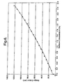
- Figure 6 shows results obtained in a test to examine the response of a mesoporous Pd device (20mC deposition, operated at 5.5V) to a series of increasing methane concentrations of up to 2.5% (averaged over about 2.5 mins at each concentration). From Figure 6 it is clear that the bridge output is a near-linear function of concentration even in the absence of a diffusion limiting housing around the sensor.
- the graph shows a second-order regression line fitted to the experimental data for illustrative purposes only.
- Figure 7 indicates that a mesoporous Pd device (20mC deposition, operated at 5.5V) subjected to repeated exposures to air and 2.5% methane exhibits good reproducibility of response over 6 cycles, and recovers to the original baseline quite reliably in each case.
- Figure 8 the output stability was again found to be quite acceptable, with good recovery back to the original air baseline.
- micromachined devices are capable of producing a stable, fast and reproducible response to methane, with a stable zero gas baseline.
- the sensitivity and power consumption of (a) the experimental mesoporous devices, (b) conventional low power coil elements and (c) a planar device known as the Microsens Catalytic Gas Sensor MCGS-2101 made by Microsens S.A. have been tabulated below: Parameter Experimental Device Conventional coil Microsens Planar Device Sensitivity (mV/% methane) 60 40 24 Power Consumption (mW per element) 165 125 30
- Figure 10 compares the relative sensitivities to 2.5% methane in air (with 100ppm hydrogen sulphide 50 and without hydrogen sulphide 51) of two planar devices coated in the mesoporous Pd catalyst. The results confirm that, as is the case for the best current commercial wirewound pellistors, the presence of the H 2 S has negligible effect upon the methane sensitivity over periods of many minutes.
Landscapes
- Chemical & Material Sciences (AREA)
- Chemical Kinetics & Catalysis (AREA)
- Electrochemistry (AREA)
- Engineering & Computer Science (AREA)
- Materials Engineering (AREA)
- Metallurgy (AREA)
- Organic Chemistry (AREA)
- General Health & Medical Sciences (AREA)
- Health & Medical Sciences (AREA)
- Life Sciences & Earth Sciences (AREA)
- Analytical Chemistry (AREA)
- Biochemistry (AREA)
- Physics & Mathematics (AREA)
- General Physics & Mathematics (AREA)
- Immunology (AREA)
- Pathology (AREA)
- Non-Reversible Transmitting Devices (AREA)
- Details Of Aerials (AREA)
- Cooling Or The Like Of Semiconductors Or Solid State Devices (AREA)
- Catalysts (AREA)
- Physical Or Chemical Processes And Apparatus (AREA)
- Investigating Or Analyzing Materials By The Use Of Electric Means (AREA)
- Resistance Heating (AREA)
- Inert Electrodes (AREA)
- Control Of Motors That Do Not Use Commutators (AREA)
Abstract
Description
- The method relates to a method of manufacturing a pellistor.
- Pellistors are catalytic oxidation sensors which measure concentrations of combustible gases in air up to the lower explosive limit. The sensors are matched in pairs of elements, each conventionally comprising a platinum wire coil embedded within a catalytic bead. An active detector element oxidises combustible gases, while an inert reference element, named the compensator, compensates for changes in ambient conditions. The coil serves two purposes. Firstly, in the detector and compensator it is used to heat the bead electrically to its operating temperature (about 500°C); and secondly, for the detector, it is also used to detect changes in temperature produced by the oxidation of the flammable gas.
- A Wheatstone Bridge circuit is used to measure the concentration of combustible gas in air. The Bridge is balanced by a variable resistance, with both elements at their operating temperature; an out-of-balance signal is produced when a combustible gas is detected. The signal is proportional to the concentration of combustible gas.
- More recently, attempts have been made to manufacture planar pellistor arrangements in which the conventional coil is replaced by a planar electrode on an inert substrate such as silicon. Typically, the silicon is micro machined to provide a thin membrane on which the heater is deposited. This is described in "Microsensors, Principles and Applications", Julian W. Gardner, pages 242-243, published by John Wiley & Sons. Potentially, planar arrangements could provide a number of important benefits. These are as follows:
- Lower power: Conventional coil pellistors can only be produced with power consumption down to about 100mW per element (i.e. 200mW per pair). The platinum wire diameter to wind coils for these power levels is about 10µm. This is the practical lower limit at which it is possible to work, due to a combination of visibility and other handling difficulties. Micro machining is capable of fabrication down to much smaller dimensions and device powers of between 1/3 to 2/3 those of conventional devices have been achieved (e.g. a device manufactured by Microsens S.A. has a specification of 60mW (25mA at 2.4 volts) for a detector/compensator pair). The ability to integrate two or more elements (i.e. a detector/compensator pair) in very close proximity can also provide economies in power consumption.
- Volume production: Conventional coil pellistor manufacture is an inherently labour intensive operation and is fundamentally not amenable to scale up for volume production. Micro machining, by its very nature, is a volume production method of fabrication and less suited to small-scale operation due to the high capital investment required. Depending on the exact technique employed, however, there are numerous contractors able to undertake production runs of different sizes. In principle, micro machined devices could be manufactured more consistently and cost effectively than conventional devices for a volume market. Even for relatively low volume industrial markets there would be a manufacturing advantage to the micro machined products which could produce more consistent quality devices with an automated method of fabrication and might offset any increased production cost associated with relatively small batch sizes.
- Improved sensitivity: Conventional coil technology limits the type of material which can be employed due to the mechanical requirements placed upon the wire. In micro machined devices, it is common to employ encapsulated heaters, hence allowing the possibility of employing materials with more favourable properties. For example, metals or alloys with higher temperature coefficients of resistance than the normally employed Pt may offer improved resolution.
-
- Pellistors have so far found applications in industrial areas to provide a warning of combustible gas accumulation to explosive levels, e.g. oil rigs, mines, sewers and other confined spaces. These markets are relatively small and suited to conventional pellistors. Other markets exist for lower cost devices, such as domestic applications which have so far been addressed by semiconductor devices. However, these suffer from well known shortcomings in performance, which severely limit their applicability.
- The catalytic coatings produced on planar devices have usually been laid down onto the micro mechanical heater substrates with coating methods (such as vapour deposition or sputtering) which result in a relatively low surface area catalyst layer. This tends to produce devices whose catalytic activity is inherently poor and which have comparatively short operational lifetimes compared to conventional pellistors. This is particularly true when such devices are operated in environments containing materials which poison and/or inhibit the catalyst surface, e.g. silicone vapours, hydrogen sulphide. It is well known that the poison resistance in such devices is greatly enhanced by using high surface area catalysts which offer some redundancy of sites.
- Attempts have been made to coat the micro machined planar heater substrates with conventional catalyst material mixes, but it is very difficult to do this accurately on areas with dimensions well below 1mm, as is often required on micro machined devices. Furthermore, the micromachined heaters are unlikely to have sufficient mechanical strength to allow conventional methods (requiring contact with the substrate) to be employed, despite the fact that they may have excellent performance in response to thermal or mechanical shock. Additionally, the adhesion of the catalyst to the substrate is generally very poor. In extreme cases, the catalyst layer breaks away from the substrate resulting in total device failure, and/or heat transfer from the substrate to the catalyst is poor, resulting in higher power consumption to maintain the catalyst at its optimum operating temperature.
- In accordance with the present invention, a method of manufacturing a pellistor comprises providing a porous catalyst layer on a heater by electrodepositing material from a mixture containing the catalyst and a structure-directing agent in an amount sufficient to form an homogenous lyotropic liquid crystalline phase in the mixture.
- We have realised that it is possible to achieve very good porous catalyst layers having high surface areas using an electrodepositing technique. Although this is particularly suitable for use with planar pellistors and thus micro machined structures, the technique could also be applied to non-planar substrate geometries including conventional coil heaters.
- We have found that the new catalyst layer can withstand the high temperatures associated with pellistor operation and is also durable and substantially poison resistant.
- The process enables closely controlled porous catalyst layers to be laid down, if required in very small regions such as less than 100µm2, for example down to about 50µm2. Typical pore sizes are in the mesoporous range with internal diameters from 13 to 200 Angstroms, preferably 17 to 40 Angstroms.
- It should be noted in particular that this method allows the amount and location of catalyst to be optimised in contrast to conventional pellistors where the bead is required to provide a support for the catalyst and introduces a significant heat sink thus requiring wasteful power input. The invention, in contrast, provides a substantially pure catalyst layer without any other material being present to act as a heat sink.
- The material may be deposited onto the heater through a mask to provide even further control of the deposit area.
- A particularly useful technique is described by Attard et al in "Mesoporous Platinum Films from Lyotropic Liquid Crystalline Phases", Science, Vol. 278, 31 October 1997, pages 838-840.
- The structure-directing agent is included in the mixture in order to impart an homogeneous lyotropic liquid crystalline phase to the mixture. The liquid crystalline phase is thought to function as a structure-directing medium or template for film deposition. By controlling the nanostructure of the lyotropic liquid crystalline phase, and electrodepositing, a film may be synthesised having a corresponding nanostructure. For example, films deposited from normal topology hexagonal phases will have a system of pores disposed on an hexagonal lattice, whereas films deposited from normal topology cubic phases will have a system of pores disposed in cubic topology. Similarly, films having lamellar nanostructures may be deposited from lamellar phases.
- Accordingly, by exploiting the rich lyotropic polymorphism exhibited by liquid crystalline phases, precise control over the structure of the films is achieved, enabling the synthesis of well-defined porous films having a long range spatially and orientationally periodic distribution of uniformly sized pores.
- Any suitable amphiphilic organic compound or compounds capable of forming an homogeneous lyotropic liquid crystalline phase may be used as the structure-directing agent, either low molar mass or polymeric. These may include compounds sometimes referred to as organic directing agents. In order to provide the necessary homogeneous liquid crystalline phase, the amphiphilic compound will generally be used at a high concentration, typically at least about 10% by weight, preferably at least 20% by weight, and more preferably at least 30% by weight, based on the total weight of the solvent and amphiphilic compound.
- Suitable compounds include organic surfactant compounds of the formula RQ wherein R represents a linear or branched alkyl, aryl, aralkyl or alkylaryl group having from 6 to about 60 carbon atoms, preferably from 12 to 18 carbon atoms, and Q represents a group selected from: [O(CH2)m]n)OH wherein m is an integer from 1 to about 4 and preferably m is 2, and n is an integer from 2 to about 60, preferably from 4 to 8; nitrogen bonded to at least one group selected from alkyl having at least four carbon atoms, aryl, aralkyl, and alkylaryl; and phosphorus or sulphur bonded to at least two oxygen atoms.
- Other suitable structure-directing agents include monoglycerides, phospholipids and glycolipids.
- Preferably, non-ionic surfactants such as octaethylene glycol monododecyl ether (C12EO8, wherein EO represents ethylene oxide) and octaethylene glycol monohexadecyl ether (C16EO8) are used as structure-directing agents.
- Further details of preferred aspects of this method are described in WO 99/00536, the content of which is included herein by reference.
- Any conventional catalyst can be used, typical examples including palladium, platinum, iridium and rhodium. In addition, mixtures of two or more of these could be used while one or more could be codeposited together with a support such as alumina or silica.
- In the case of a planar electrode, this may be in a serpentine form in order to increase the length of the electrode within a predefined area.
- The ability to localise the catalyst in the regions where the heater is known to be operating at maximum efficiency optimises the sensitivity obtained per unit power input.
- In general, prior to the electrodepositing step, the method comprises providing an electrode on the heater structure which contacts the mixture during the electrodepositing process. This enables the region of deposit to be controlled and also separates the components involved with the electrodepositing step from the heater structure. However, it may be possible in some circumstances to use the conductor forming the heater as one of the electrodes which is used during the electrodepositing step.
- Some examples of pellistors according to the invention and methods for their manufacture will now be described with reference to the accompanying drawings in which:-
- Figure 1 is a schematic cross-section through a partially manufactured pellistor;
- Figure 2 is a plan of the pellistor shown in Figure 1 prior to provision of the catalyst layer;
- Figure 3 is a schematic side view illustrating the provision of the catalyst layer;
- Figure 4 illustrates a Wheatstone bridge circuit used to test the performance of the pellistor;
- Figure 5 illustrates graphically the change in bridge output (corrected for baseline shift with detector voltage) against detector voltage in response to 2.5% methane for two different pellistors;
- Figure 6 illustrates the variation of mean bridge output with methane concentration;
- Figure 7 illustrates the variation of bridge output with time during repeated exposures to 0% and 2.5% methane in air;
- Figure 8 illustrates the variation of bridge output with time during extended exposure to 2.5% methane in air;
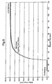
- Figure 9 illustrates the initial portion of Figure 8 in enlarged detail; and,
- Figure 10 illustrates the poison resistance of the pellistor.
-
- The partially manufactured pellistor illustrated in Figure 1 comprises a silicon substrate 1 on which has been deposited a layer of silicon nitride 2 (or silicon oxynitride). A serpentine,
platinum electrode 5 has been vacuum deposited onto thesilicon nitride layer 2. A furthersilicon nitride layer 6 is then provided over theelectrode 5 as an inert encapsulation. The overall thickness of thissilicon nitride layer 6 is less than 1 micron, for example 0.3 microns. The ends of theelectrode 5 are electrically coupled to a pair ofcontact pads - In order for the device to function as a pellistor, it is necessary to provide a catalyst layer to promote combustion of the gas to be detected. To achieve this, a mask (not shown) defining the geometry and position of an electrode is provided on the
layer 6 using standard photo lithographic techniques. A further electrode ofgold 9 is then vacuum deposited through the mask onto part of thesilicon nitride layer 6 overlying the turns of theelectrode 5. Theelectrode 9 is coupled to acontact pad 10. One of the important aspects of this invention is the ability to localise the provision of thecatalyst layer 11 and this is achieved by limiting the size of theelectrode 9 since the catalyst layer will only deposit onto theelectrode 9. The mask is then removed. - As an alternative to gold, platinum or palladium or highly doped amorphous silicon could be used.
- At this stage the silicon substrate 1 is micromachined at 3 so that a
thin membrane 4 of silicon nitride is defined having a thickness of about 0.3µ. The membrane has typical lateral dimensions of 2mm x 2mm. The thin membrane reduces heat loss from the heater so that it has a low heat capacity leading to a very fast time constant and low power consumption. - A suitable catalyst/liquid crystal mixture is then prepared and this can be based on any of the examples described in the Attard et al paper mentioned above and in the preferred case the mixture is as follows:
- pure deionized water
- heptane
- palladium salt : ammonium tetrachloropalladate
- liquid crystal template: octaethylene glycol
monohexadecyl ether, formulae can be:,
- the ratios used were: %(wt) template: 55%
%(wt) water: 45% - the ratio salt to water in weight was around 0.3 the ratio of heptane was 4 moles of template to 1 mole of heptane.
- This leads to the quantities listed below:
- template: 400 mg
- heptane: 16.9 mg
- water : 327.3 mg
- salt : 98.2 mg
-
- After weighing the template, the process involves adding the heptane, adding the water and then adding the palladium salt. The solution then needs to be mixed to make sure it is a homogeneous thick brownish paste. In a simple approach illustrated schematically in Figure 3, the mixture is then fed into a
pipette 20 so as to form adrop 21 into which extends aPt counter electrode 22. A voltage is applied across theelectrode 22 and theelectrode 9 and as aresult material 11 is deposited onto theelectrode 9. The deposit comprises two interpenetrating phases of template and catalyst materials each with very well controlled, uniform high surface area structures. The template component can then be removed with acid or the like although it is thought that this is not always necessary. - In the preferred technique, an
additional reference electrode 30 such as a Saturated Calomel Electrode (SCE) is used, the electrical "contact" between the three electrodes being made via glass frits 31,32. The additional use of the third (reference) electrode allows greater control of the potentials during the deposition and subsequent conditioning processes. - Deposition was always done at room temperature at 100mV vs SCE. The amount of charge passed to make a working gas sensor is around 20mC.
- In some cases, the mixture could be deposited through a mask overlying the
electrode 9. Irrespective of the size of the drop (beyond the minimum required to cover the gold electrode), the catalyst will still only grow on the electrode. However, depending on the nature of the peripheral construction (e.g. the strength of the wires connecting the heater to the packaging), it can be advantageous to limit the drop size using a mask. - The deposit was then washed in deionised water for one or two hours, and then cycled in 2M H2SO4 between 0.2V and 1.1V vs SCE until the charge passed in the stripping peak of the oxide reaches a maximum.
- Experiments have been carried out on some pellistors constructed in accordance with the invention using a Wheatstone bridge circuit of the form shown in Figure 4. In this diagram, PP is the pellistor under test, Rc has a resistance of about 300Ω, RB has a resistance of about 100Ω, RT has a resistance of about 1KΩ, the total supply voltage V+ - V- is about 14.2 volts with a total bridge current of about 120mA. The current passing through the pellistor is about 30mA.
- The circuit differs from that which will be used in operation since no compensator is used. However, in the absence of a compensator, this would be expected to reduce the overall performance of the system, particularly in terms of signal stability. The resistance values in the balancing arm of the bridge have not been optimised to minimise overall power consumption in the initial experiments. It is nevertheless possible to estimate the power consumed by a single micromachined element, since the total bridge current is known, as is the voltage across the active device. This gives a value of about 165mW for operation @ 5.5V. Under these conditions the device heater resistance is about 300Ω.
- The devices tested were not placed in diffusion limiting cans or the like although such a can might be used in practice.
- Figure 5 shows the response of two prototype mesoporous Pd devices to 2.5% methane in air as a function of the operating voltage across the sensor. Although the optimum sensitivity is obtained at about 7.0V, all subsequent data discussed below was actually obtained by operating at only 5.5V in order to reduce the thermal stress on the substrates. Thus, the results quoted do not represent the optimum performance which might eventually be envisaged, albeit at the expense of increased power consumption.
- Figure 6 shows results obtained in a test to examine the response of a mesoporous Pd device (20mC deposition, operated at 5.5V) to a series of increasing methane concentrations of up to 2.5% (averaged over about 2.5 mins at each concentration). From Figure 6 it is clear that the bridge output is a near-linear function of concentration even in the absence of a diffusion limiting housing around the sensor. The graph shows a second-order regression line fitted to the experimental data for illustrative purposes only.
- Figure 7 indicates that a mesoporous Pd device (20mC deposition, operated at 5.5V) subjected to repeated exposures to air and 2.5% methane exhibits good reproducibility of response over 6 cycles, and recovers to the original baseline quite reliably in each case. In a longer exposure to the same methane concentration (Figure 8), the output stability was again found to be quite acceptable, with good recovery back to the original air baseline. Finally, Figure 9 shows the early stages of this test in more detail and indicates that, even without allowing for the dead volume inherent in the experimental system, acceptable response times (T90 = 18secs) are obtained.
- In summary, it has been shown that the micromachined devices are capable of producing a stable, fast and reproducible response to methane, with a stable zero gas baseline.
- The sensitivity and power consumption of (a) the experimental mesoporous devices, (b) conventional low power coil elements and (c) a planar device known as the Microsens Catalytic Gas Sensor MCGS-2101 made by Microsens S.A. have been tabulated below:
Parameter Experimental Device Conventional coil Microsens Planar Device Sensitivity (mV/% methane) 60 40 24 Power Consumption (mW per element) 165 125 30 - The effect of a well known pellistor poison has been shown to have minimal effect upon the sensitivity behaviour of the new devices. Figure 10 compares the relative sensitivities to 2.5% methane in air (with
100ppm hydrogen sulphide 50 and without hydrogen sulphide 51) of two planar devices coated in the mesoporous Pd catalyst. The results confirm that, as is the case for the best current commercial wirewound pellistors, the presence of the H2S has negligible effect upon the methane sensitivity over periods of many minutes.
Claims (14)
- A method of manufacturing a pellistor, the method comprising providing a porous catalyst layer on a heater by electrodepositing material from a mixture containing the catalyst and a structure-directing agent in an amount sufficient to form an homogenous lyotropic liquid crystalline phase in the mixture.
- A method according to claim 1, further comprising removing the structure-directing agent after the material has been deposited.
- A method according to claim 1 or claim 2, wherein the structure-directing agent comprises an amphiphilic organic compound or compounds.
- A method according to claim 3, wherein the structure-directing agent comprises octaethylene glycol monohexadecyl ether.
- A method according to any of the preceding claims, wherein the catalyst comprises one or more of palladium, platinum, iridium and rhodium.
- A method according to any of the preceding claims, wherein the mixture further comprises a solvent.
- A method according to any of the preceding claims, wherein the heater comprises a planar electrode provided on a substrate.
- A method according to claim 7, wherein the heater has a serpentine form.
- A method according to claim 7 or claim 8, wherein the substrate comprises a micro machined membrane.
- A method according to any of the preceding claims, wherein the material is deposited onto the heater through a mask.
- A method according to any of the preceding claims, wherein the material forms a catalyst layer covering an area less than 100µm2, for example about 50µm2.
- A method according to any of the preceding claims, further comprising, prior to the electrodepositing step, providing an electrode on the heater structure which contacts the mixture during the electrodepositing process.
- A method according to claim 12, wherein the electrode comprises gold.
- A method according to claim 12 or claim 13, wherein the electrode is vapour deposited onto the heater structure.
Applications Claiming Priority (3)
| Application Number | Priority Date | Filing Date | Title |
|---|---|---|---|
| GBGB9819160.4A GB9819160D0 (en) | 1998-09-02 | 1998-09-02 | Pellistor |
| GB9819160 | 1998-09-02 | ||
| PCT/GB1999/002644 WO2000014307A1 (en) | 1998-09-02 | 1999-08-11 | Pellistor |
Publications (2)
| Publication Number | Publication Date |
|---|---|
| EP1114207A1 EP1114207A1 (en) | 2001-07-11 |
| EP1114207B1 true EP1114207B1 (en) | 2002-12-04 |
Family
ID=10838245
Family Applications (1)
| Application Number | Title | Priority Date | Filing Date |
|---|---|---|---|
| EP99939517A Expired - Lifetime EP1114207B1 (en) | 1998-09-02 | 1999-08-11 | Pellistor |
Country Status (9)
| Country | Link |
|---|---|
| US (1) | US6395230B1 (en) |
| EP (1) | EP1114207B1 (en) |
| AT (1) | ATE229100T1 (en) |
| AU (1) | AU5378899A (en) |
| CA (1) | CA2341033A1 (en) |
| DE (1) | DE69904349T2 (en) |
| GB (1) | GB9819160D0 (en) |
| WO (1) | WO2000014307A1 (en) |
| ZA (1) | ZA200101225B (en) |
Families Citing this family (9)
| Publication number | Priority date | Publication date | Assignee | Title |
|---|---|---|---|---|
| US7776379B2 (en) * | 2001-09-19 | 2010-08-17 | Medlogics Device Corporation | Metallic structures incorporating bioactive materials and methods for creating the same |
| US6812708B2 (en) * | 2002-06-04 | 2004-11-02 | Scott Technologies, Inc. | Combustible-gas measuring instrument |
| US7001669B2 (en) * | 2002-12-23 | 2006-02-21 | The Administration Of The Tulane Educational Fund | Process for the preparation of metal-containing nanostructured films |
| GB0400166D0 (en) * | 2004-01-06 | 2004-02-11 | Ic Innovations Ltd | Catalyst |
| GB0500035D0 (en) * | 2005-01-04 | 2005-02-09 | Nanotecture Ltd | Filter |
| GB2441531A (en) * | 2006-09-08 | 2008-03-12 | Nanotecture Ltd | Liquid crystal templated deposition method |
| US7833482B2 (en) | 2006-12-29 | 2010-11-16 | Honeywell International Inc. | Low power combustible gas sensor |
| US8024958B2 (en) | 2007-05-18 | 2011-09-27 | Life Safety Distribution Ag | Gas sensors with thermally insulating ceramic substrates |
| JP7452024B2 (en) * | 2020-01-17 | 2024-03-19 | 富士電機株式会社 | electronic equipment |
Family Cites Families (12)
| Publication number | Priority date | Publication date | Assignee | Title |
|---|---|---|---|---|
| US4070207A (en) * | 1976-10-19 | 1978-01-24 | Holdeman Louis B | Method of producing porous copper workpieces and product thereof |
| ES2009404A6 (en) * | 1988-11-24 | 1989-09-16 | Quintela Manuel Arturo Lopez | Process to obtain fine magnetic Nd-Fe-B particles of various sizes. |
| US4977038A (en) * | 1989-04-14 | 1990-12-11 | Karl Sieradzki | Micro- and nano-porous metallic structures |
| US5837639A (en) * | 1990-01-25 | 1998-11-17 | Mobil Oil Corporation | Hydroprocessing catalyst |
| GB9301104D0 (en) | 1993-01-21 | 1993-03-10 | Servomex Plc | Sensor for combustible gases |
| WO1995010770A1 (en) * | 1993-10-08 | 1995-04-20 | Csir | A catalytic gas sensor |
| US5712402A (en) * | 1994-08-22 | 1998-01-27 | Board Of Trustees Operating Michigan State University | Catalytic applications of mesoporous metallosilicate molecular sieves and methods for their preparation |
| AU5382796A (en) * | 1995-04-03 | 1996-10-23 | Massachusetts Institute Of Technology | Composition and method for producing hexagonally-packed meso porous metal oxide |
| US5718878A (en) * | 1996-07-12 | 1998-02-17 | Akzo Nobel N.V. | Mesoporous titania and process for its preparation |
| DE19705497C2 (en) * | 1997-02-13 | 1999-01-28 | Max Planck Gesellschaft | Process for the preparation of mesoporous solids, solids obtainable by the process and their use |
| GB9703920D0 (en) * | 1997-02-25 | 1997-04-16 | Univ Southampton | Method of preparing a porous metal |
| US6056545A (en) * | 1999-04-20 | 2000-05-02 | Lemchen; Marc. S. | Mesoporous metal for orthodontic appliances |
-
1998
- 1998-09-02 GB GBGB9819160.4A patent/GB9819160D0/en not_active Ceased
-
1999
- 1999-08-11 DE DE69904349T patent/DE69904349T2/en not_active Expired - Lifetime
- 1999-08-11 US US09/762,690 patent/US6395230B1/en not_active Expired - Lifetime
- 1999-08-11 AU AU53788/99A patent/AU5378899A/en not_active Abandoned
- 1999-08-11 WO PCT/GB1999/002644 patent/WO2000014307A1/en not_active Ceased
- 1999-08-11 AT AT99939517T patent/ATE229100T1/en not_active IP Right Cessation
- 1999-08-11 CA CA002341033A patent/CA2341033A1/en not_active Abandoned
- 1999-08-11 EP EP99939517A patent/EP1114207B1/en not_active Expired - Lifetime
-
2001
- 2001-02-13 ZA ZA200101225A patent/ZA200101225B/en unknown
Also Published As
| Publication number | Publication date |
|---|---|
| DE69904349T2 (en) | 2003-04-17 |
| AU5378899A (en) | 2000-03-27 |
| ATE229100T1 (en) | 2002-12-15 |
| DE69904349D1 (en) | 2003-01-16 |
| GB9819160D0 (en) | 1998-10-28 |
| EP1114207A1 (en) | 2001-07-11 |
| WO2000014307A1 (en) | 2000-03-16 |
| CA2341033A1 (en) | 2000-03-16 |
| ZA200101225B (en) | 2002-04-24 |
| US6395230B1 (en) | 2002-05-28 |
Similar Documents
| Publication | Publication Date | Title |
|---|---|---|
| KR100449069B1 (en) | Microelectrode, microelectrode array and a method for manufacturing the microelectrode | |
| EP1552272B1 (en) | Palladium-silver alloy nanowires and nanoparticle columns for use as variable-range hydrogen sensors | |
| US7237429B2 (en) | Continuous-range hydrogen sensors | |
| CA2326210C (en) | Hydrogen gas sensor | |
| US6395230B1 (en) | Pellistor | |
| EP1226090B1 (en) | Gas sensor and fabrication method thereof | |
| JPH08505227A (en) | Nanostructured electrode membrane | |
| JP2014528590A (en) | Sensor and sensor manufacturing method | |
| CN1085338C (en) | Combustible gas sensor and method for fabricating the same | |
| US20190100851A1 (en) | Thermochemical Gas Sensor Using Thermoelectric Thin Film And Method Of Manufacturing The Same | |
| US20020187075A1 (en) | Hydrogen sensor | |
| JPH04507461A (en) | Self-holding thin film filament sensor, its formation method, and application to gas detectors and gas chromatography | |
| US20080035476A1 (en) | Interdigitated Electrochemical Gas Generator | |
| KR19980080155A (en) | Sensor with thin film member | |
| EP0056339B1 (en) | A method of producing a stannic oxide type gas-detecting device | |
| JP5275099B2 (en) | Hydrogen detection element and hydrogen detection sensor | |
| CN118387829A (en) | Preparation method of hydrogen sensor based on nickel oxide quantum dot material | |
| US7736479B2 (en) | Electrochemical sensor having nonporous working electrode | |
| Tuller et al. | Photo-assisted silicon micromachining: opportunities for chemical sensing | |
| JPH10300718A5 (en) | ||
| CN114008449A (en) | Transistor comprising ceramic and ionic gel | |
| Wang et al. | Humidity Sensing of Ordered Macroporous Silicon With ${\rm HfO} _ {2} $ Thin-Film Surface Coating | |
| JP2006284327A (en) | Hydrogen gas sensor | |
| EP0697593A1 (en) | Low power catalytic combustible gas detector | |
| Vayenas et al. | In situ controlled promotion of catalyst surfaces via solid electrolytes: The NEMCA effect |
Legal Events
| Date | Code | Title | Description |
|---|---|---|---|
| PUAI | Public reference made under article 153(3) epc to a published international application that has entered the european phase |
Free format text: ORIGINAL CODE: 0009012 |
|
| 17P | Request for examination filed |
Effective date: 20010327 |
|
| AK | Designated contracting states |
Kind code of ref document: A1 Designated state(s): AT BE CH CY DE DK ES FI FR GB GR IE IT LI LU MC NL PT SE |
|
| AX | Request for extension of the european patent |
Free format text: AL;LT;LV;MK;RO;SI |
|
| 17Q | First examination report despatched |
Effective date: 20010821 |
|
| GRAG | Despatch of communication of intention to grant |
Free format text: ORIGINAL CODE: EPIDOS AGRA |
|
| GRAG | Despatch of communication of intention to grant |
Free format text: ORIGINAL CODE: EPIDOS AGRA |
|
| GRAH | Despatch of communication of intention to grant a patent |
Free format text: ORIGINAL CODE: EPIDOS IGRA |
|
| GRAH | Despatch of communication of intention to grant a patent |
Free format text: ORIGINAL CODE: EPIDOS IGRA |
|
| GRAA | (expected) grant |
Free format text: ORIGINAL CODE: 0009210 |
|
| AK | Designated contracting states |
Kind code of ref document: B1 Designated state(s): AT BE CH CY DE DK ES FI FR GB GR IE IT LI LU MC NL PT SE |
|
| PG25 | Lapsed in a contracting state [announced via postgrant information from national office to epo] |
Ref country code: NL Free format text: LAPSE BECAUSE OF FAILURE TO SUBMIT A TRANSLATION OF THE DESCRIPTION OR TO PAY THE FEE WITHIN THE PRESCRIBED TIME-LIMIT Effective date: 20021204 Ref country code: IT Free format text: LAPSE BECAUSE OF FAILURE TO SUBMIT A TRANSLATION OF THE DESCRIPTION OR TO PAY THE FEE WITHIN THE PRESCRIBED TIME-LIMIT;WARNING: LAPSES OF ITALIAN PATENTS WITH EFFECTIVE DATE BEFORE 2007 MAY HAVE OCCURRED AT ANY TIME BEFORE 2007. THE CORRECT EFFECTIVE DATE MAY BE DIFFERENT FROM THE ONE RECORDED. Effective date: 20021204 Ref country code: GR Free format text: LAPSE BECAUSE OF FAILURE TO SUBMIT A TRANSLATION OF THE DESCRIPTION OR TO PAY THE FEE WITHIN THE PRESCRIBED TIME-LIMIT Effective date: 20021204 Ref country code: FI Free format text: LAPSE BECAUSE OF FAILURE TO SUBMIT A TRANSLATION OF THE DESCRIPTION OR TO PAY THE FEE WITHIN THE PRESCRIBED TIME-LIMIT Effective date: 20021204 Ref country code: BE Free format text: LAPSE BECAUSE OF FAILURE TO SUBMIT A TRANSLATION OF THE DESCRIPTION OR TO PAY THE FEE WITHIN THE PRESCRIBED TIME-LIMIT Effective date: 20021204 Ref country code: AT Free format text: LAPSE BECAUSE OF FAILURE TO SUBMIT A TRANSLATION OF THE DESCRIPTION OR TO PAY THE FEE WITHIN THE PRESCRIBED TIME-LIMIT Effective date: 20021204 |
|
| REF | Corresponds to: |
Ref document number: 229100 Country of ref document: AT Date of ref document: 20021215 Kind code of ref document: T |
|
| REG | Reference to a national code |
Ref country code: GB Ref legal event code: FG4D |
|
| REG | Reference to a national code |
Ref country code: CH Ref legal event code: NV Representative=s name: ISLER & PEDRAZZINI AG Ref country code: CH Ref legal event code: EP |
|
| REG | Reference to a national code |
Ref country code: IE Ref legal event code: FG4D |
|
| REF | Corresponds to: |
Ref document number: 69904349 Country of ref document: DE Date of ref document: 20030116 |
|
| PG25 | Lapsed in a contracting state [announced via postgrant information from national office to epo] |
Ref country code: SE Free format text: LAPSE BECAUSE OF FAILURE TO SUBMIT A TRANSLATION OF THE DESCRIPTION OR TO PAY THE FEE WITHIN THE PRESCRIBED TIME-LIMIT Effective date: 20030304 Ref country code: DK Free format text: LAPSE BECAUSE OF FAILURE TO SUBMIT A TRANSLATION OF THE DESCRIPTION OR TO PAY THE FEE WITHIN THE PRESCRIBED TIME-LIMIT Effective date: 20030304 |
|
| PG25 | Lapsed in a contracting state [announced via postgrant information from national office to epo] |
Ref country code: PT Free format text: LAPSE BECAUSE OF FAILURE TO SUBMIT A TRANSLATION OF THE DESCRIPTION OR TO PAY THE FEE WITHIN THE PRESCRIBED TIME-LIMIT Effective date: 20030305 |
|
| NLV1 | Nl: lapsed or annulled due to failure to fulfill the requirements of art. 29p and 29m of the patents act | ||
| LTIE | Lt: invalidation of european patent or patent extension |
Effective date: 20021204 |
|
| PG25 | Lapsed in a contracting state [announced via postgrant information from national office to epo] |
Ref country code: ES Free format text: LAPSE BECAUSE OF FAILURE TO SUBMIT A TRANSLATION OF THE DESCRIPTION OR TO PAY THE FEE WITHIN THE PRESCRIBED TIME-LIMIT Effective date: 20030627 |
|
| ET | Fr: translation filed | ||
| PG25 | Lapsed in a contracting state [announced via postgrant information from national office to epo] |
Ref country code: LU Free format text: LAPSE BECAUSE OF NON-PAYMENT OF DUE FEES Effective date: 20030811 Ref country code: IE Free format text: LAPSE BECAUSE OF NON-PAYMENT OF DUE FEES Effective date: 20030811 Ref country code: CY Free format text: LAPSE BECAUSE OF FAILURE TO SUBMIT A TRANSLATION OF THE DESCRIPTION OR TO PAY THE FEE WITHIN THE PRESCRIBED TIME-LIMIT Effective date: 20030811 |
|
| PG25 | Lapsed in a contracting state [announced via postgrant information from national office to epo] |
Ref country code: MC Free format text: LAPSE BECAUSE OF NON-PAYMENT OF DUE FEES Effective date: 20030831 |
|
| PLBE | No opposition filed within time limit |
Free format text: ORIGINAL CODE: 0009261 |
|
| STAA | Information on the status of an ep patent application or granted ep patent |
Free format text: STATUS: NO OPPOSITION FILED WITHIN TIME LIMIT |
|
| 26N | No opposition filed |
Effective date: 20030905 |
|
| REG | Reference to a national code |
Ref country code: IE Ref legal event code: MM4A |
|
| REG | Reference to a national code |
Ref country code: CH Ref legal event code: PCAR Free format text: ISLER & PEDRAZZINI AG;POSTFACH 1772;8027 ZUERICH (CH) |
|
| PGFP | Annual fee paid to national office [announced via postgrant information from national office to epo] |
Ref country code: CH Payment date: 20070709 Year of fee payment: 9 |
|
| REG | Reference to a national code |
Ref country code: CH Ref legal event code: PL |
|
| PG25 | Lapsed in a contracting state [announced via postgrant information from national office to epo] |
Ref country code: LI Free format text: LAPSE BECAUSE OF NON-PAYMENT OF DUE FEES Effective date: 20080831 Ref country code: CH Free format text: LAPSE BECAUSE OF NON-PAYMENT OF DUE FEES Effective date: 20080831 |
|
| REG | Reference to a national code |
Ref country code: FR Ref legal event code: PLFP Year of fee payment: 17 |
|
| PGFP | Annual fee paid to national office [announced via postgrant information from national office to epo] |
Ref country code: FR Payment date: 20150624 Year of fee payment: 17 |
|
| PGFP | Annual fee paid to national office [announced via postgrant information from national office to epo] |
Ref country code: DE Payment date: 20150831 Year of fee payment: 17 Ref country code: GB Payment date: 20150728 Year of fee payment: 17 |
|
| REG | Reference to a national code |
Ref country code: DE Ref legal event code: R119 Ref document number: 69904349 Country of ref document: DE |
|
| GBPC | Gb: european patent ceased through non-payment of renewal fee |
Effective date: 20160811 |
|
| REG | Reference to a national code |
Ref country code: FR Ref legal event code: ST Effective date: 20170428 |
|
| PG25 | Lapsed in a contracting state [announced via postgrant information from national office to epo] |
Ref country code: DE Free format text: LAPSE BECAUSE OF NON-PAYMENT OF DUE FEES Effective date: 20170301 Ref country code: GB Free format text: LAPSE BECAUSE OF NON-PAYMENT OF DUE FEES Effective date: 20160811 Ref country code: FR Free format text: LAPSE BECAUSE OF NON-PAYMENT OF DUE FEES Effective date: 20160831 |