EP1113522A2 - Coupling structure of waveguide and applicator, and its application to electrodeless lamp - Google Patents
Coupling structure of waveguide and applicator, and its application to electrodeless lamp Download PDFInfo
- Publication number
- EP1113522A2 EP1113522A2 EP00116103A EP00116103A EP1113522A2 EP 1113522 A2 EP1113522 A2 EP 1113522A2 EP 00116103 A EP00116103 A EP 00116103A EP 00116103 A EP00116103 A EP 00116103A EP 1113522 A2 EP1113522 A2 EP 1113522A2
- Authority
- EP
- European Patent Office
- Prior art keywords
- waveguide
- electromagnetic wave
- applicator
- coupling structure
- structure according
- Prior art date
- Legal status (The legal status is an assumption and is not a legal conclusion. Google has not performed a legal analysis and makes no representation as to the accuracy of the status listed.)
- Granted
Links
- 230000008878 coupling Effects 0.000 title claims abstract description 55
- 238000010168 coupling process Methods 0.000 title claims abstract description 55
- 238000005859 coupling reaction Methods 0.000 title claims abstract description 55
- 230000000750 progressive effect Effects 0.000 claims description 7
- 230000005684 electric field Effects 0.000 description 14
- 238000009826 distribution Methods 0.000 description 6
- 238000010438 heat treatment Methods 0.000 description 4
- 230000001902 propagating effect Effects 0.000 description 4
- 230000005540 biological transmission Effects 0.000 description 3
- 230000005672 electromagnetic field Effects 0.000 description 3
- 239000007788 liquid Substances 0.000 description 3
- 230000010287 polarization Effects 0.000 description 3
- OKTJSMMVPCPJKN-UHFFFAOYSA-N Carbon Chemical compound [C] OKTJSMMVPCPJKN-UHFFFAOYSA-N 0.000 description 2
- RTZKZFJDLAIYFH-UHFFFAOYSA-N Diethyl ether Chemical compound CCOCC RTZKZFJDLAIYFH-UHFFFAOYSA-N 0.000 description 2
- 238000000034 method Methods 0.000 description 2
- 230000004048 modification Effects 0.000 description 2
- 238000012986 modification Methods 0.000 description 2
- 239000004809 Teflon Substances 0.000 description 1
- 229920006362 Teflon® Polymers 0.000 description 1
- 230000002159 abnormal effect Effects 0.000 description 1
- 238000010521 absorption reaction Methods 0.000 description 1
- 230000000903 blocking effect Effects 0.000 description 1
- 229910052799 carbon Inorganic materials 0.000 description 1
- 230000008859 change Effects 0.000 description 1
- 239000004020 conductor Substances 0.000 description 1
- 230000000593 degrading effect Effects 0.000 description 1
- 230000001066 destructive effect Effects 0.000 description 1
- 239000000284 extract Substances 0.000 description 1
- 230000002349 favourable effect Effects 0.000 description 1
- 229910002804 graphite Inorganic materials 0.000 description 1
- 239000010439 graphite Substances 0.000 description 1
- 239000012212 insulator Substances 0.000 description 1
- 230000003993 interaction Effects 0.000 description 1
- 238000004519 manufacturing process Methods 0.000 description 1
- 239000000463 material Substances 0.000 description 1
- 238000002360 preparation method Methods 0.000 description 1
- 238000009877 rendering Methods 0.000 description 1
- 238000004904 shortening Methods 0.000 description 1
- 239000007787 solid Substances 0.000 description 1
- XLYOFNOQVPJJNP-UHFFFAOYSA-N water Substances O XLYOFNOQVPJJNP-UHFFFAOYSA-N 0.000 description 1
- 229910001868 water Inorganic materials 0.000 description 1
Images




Classifications
-
- H—ELECTRICITY
- H01—ELECTRIC ELEMENTS
- H01P—WAVEGUIDES; RESONATORS, LINES, OR OTHER DEVICES OF THE WAVEGUIDE TYPE
- H01P5/00—Coupling devices of the waveguide type
- H01P5/12—Coupling devices having more than two ports
- H01P5/16—Conjugate devices, i.e. devices having at least one port decoupled from one other port
- H01P5/18—Conjugate devices, i.e. devices having at least one port decoupled from one other port consisting of two coupled guides, e.g. directional couplers
- H01P5/181—Conjugate devices, i.e. devices having at least one port decoupled from one other port consisting of two coupled guides, e.g. directional couplers the guides being hollow waveguides
-
- H—ELECTRICITY
- H01—ELECTRIC ELEMENTS
- H01J—ELECTRIC DISCHARGE TUBES OR DISCHARGE LAMPS
- H01J65/00—Lamps without any electrode inside the vessel; Lamps with at least one main electrode outside the vessel
Definitions
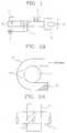
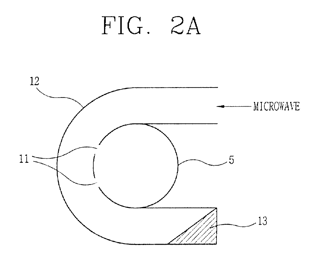
- the actual effective length of the waveguide 12 starts from one side of the wall 9 installed within the waveguide and ends at the opposite side of the wall 9 in the circumferential direction.
- the waveguide is formed as long as integer times the half of the wave length (that is, n ⁇ /2, 'n' is integer) inside the waveguide, the waveguide itself is able to serve as a resonator.
- the electromagnetic wave within the waveguide propagates along a circular trajectory and is transmitted to the resonator through the coupling slot installed on the wall held in common by the waveguide and the resonator, so as to be applied to the load therein.
- the waveguide serves as a resonator (termed as a 'first resonator', hereinafter), a stable operation state can be maintained according to the state of the load inside the applicator.
- standing wave is generated in the waveguide, that is, the first resonator, before the bulb is completely ignited, and the second resonator is excited by the standing wave.
- a resonator is formed by blocking both ends of the waveguide of which electrical length is the same as the guided wave length thereof.
- the waveguide has a rectangular cross section, it corresponds to a resonator operating in the TE 102 mode, while if the waveguide has a circular cross section, it corresponds to a resonator operated in the TE 112 mode.
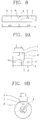
- the electromagnetic wave within the resonator forms a standing wave, and the distribution of the electric field strength 16 is shown in dotted line as illustrated in Figure 7.
- the electric field strength in the middle point of the resonator is '0', and even if this point is blocked by a conductor wall 9, there is no variation in a boundary condition, the distribution of the electric field is maintained as it is and the two spaces divided by the installed wall respectively forms independent resonators 12 and 5.
- the two resonators that is, the first and the second resonators 12 and 5 are connected to each other, still maintaining the original electric field distribution.
- the electromagnetic wave applied to the bulb is mostly absorbed by the bulb, and thus there is little electromagnetic wave turning back to the first resonator.
- the first resonator is not operated as a resonator but operated as a normal waveguide.
- An electric field strength 16 at this time is shown in dotted line as illustrated in Figure 8. At this time, there is no standing wave within the waveguide 12, so that the electric field strength 16 within the waveguide becomes even.
- the coupling slot is designed so that the electromagnetic wave within the waveguide is effectively coupled to the second resonator, and installed on the wall between the waveguide and the second resonator in the progressive direction of the electromagnetic wave. It is desirable to determine the position, length and width of the slot so a satisfactory matching is achieved when the bulb is in its normal operating state.
- a rectangularly shaped one is generally used; however, any modification to its shape is possible in view of a design object and for better performance, for example, a shape of which both end portions are round-shaped, as desired.
- the electric field rotates centered around the axis of the resonator when it is viewed in the cross-section side of the resonator, the electric field is evenly applied along the circumference of the bulb, so that a possible damage to the bulb due to a local heating on the surface of the bulb can be prevented, and accordingly, the bulb does not need to be rotated.
- Figures 10B and 10C respectively show a rectangular waveguide rolled structure over the 'E' side and 'H' side, for easy understanding.
- the waveguide and the second resonator are combined by the jointly-owned surface therebetween, that is, by the directional coupling slots installed at the 'E' side of the waveguide.
- the directional coupling slots are constructed by arrangement of four slots, which are basically an array of two independent directional coupling slot structures placed consequently, each consists of a pair of slots.
- the coupling slots are installed on the 'E' side of the waveguide, that is, the wide side.
- the reason for this is that the second resonator jointly owns a portion of 'E' side of the waveguide. If the second resonator jointly owns the 'H' side of the waveguide, that is, a part of the narrow side, the coupling slot can be also installed on the 'H' side of the waveguide.
- the waveguide is rolled in a cylindrical form over the 'E' side, it is also possible to roll in the cylindrical form over the 'H' side of the waveguide, and in both cases, it is possible to install slots on both the 'E' side and the 'H' side.
- the second resonator is of a cylinder having a diameter of approximately 75mm and operated in the TE 111 mode.
- the side wall and the front wall of the cylinder are made of a mesh screen, and its rear wall jointly owns the 'H' side of the waveguide.
- the waveguide and the second resonator are coupled by a traveling wave coupling slot installed on the 'H' side of the waveguide.
- the width of the slot is more than three times the thickness of the wall where the slot is installed. If the width of the slot is narrow, the quality factor Q becomes high, and when coupled to the unloaded resonator which is the case when the bulb inside it is cold and not ignited, the high Q of both the slot and the resonator makes it easier to ignite the bulb. However, since 'Q' of the resonator becomes much lower as the bulb is fully ignited, it is difficult to maintain a good matching in its normal operating state. Thus, the width of the slot should be determined accordingly.
- the width of the slot is approximately 12mm, and the position of the slot is determined where the matching is the most suitably made after the bulb is completely lit up.
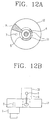
- Figures 12A and 12B show a structure of a waveguide adopted to an electrodeless lamp in accordance with yet another embodiment of the present invention.
- This embodiment is featured in that the waveguide with a rectangular cross section is rolled into cylindrical form over the 'H' side.
- the cylindrical second resonator jointly owns a part of the 'E' side of the waveguide, and the waveguide and the second resonator are coupled by the jointly-owned portion, that is, by the coupling slots installed on the 'E' side of the waveguide .
- the coupling slots operates as a directional coupling structure consists of two slots, of which the second slot is shorter than the first slot for the purpose of improving the matching characteristics.
- the overall apparatus can come inside the outer diameter of the waveguide on the basis of the axis of the bulb, which is very advantageous for designing a lamp bulb system having a cylindrical external appearance.
- the matching state of the system does not need to be adjusted to follow the variation of the load state.
- Using the tuner accompanies an inconvenience that the matching state should be adjusted according to the variation of the load state, but in the present invention, a load of different kind or different characteristics can be used without changing the system.
- the life of the electromagnetic wave generator such as magnetron is extended and the system operates stably, and thus the efficiency of the system can be remarkably improved.
- the waveguide which also serves as a resonator a stable operation state can be maintained over a wide range of load state.
- the waveguide and the resonator guarantee ignition and support of stable discharge, and the phenomenon of system failure can be prevented during the mode switching.
- the reflected wave is prevented from turning back to the magnetron and the rotational polarization can be excited into the resonator. Accordingly, the uniformity of the electromagnetic field distribution within the resonator is improved, so that the plasma discharge inside the bulb is stably maintained, and as the necessity of rotating the bulb is reduced, a damage to the bulb can be prevented.
Landscapes
- Physics & Mathematics (AREA)
- Engineering & Computer Science (AREA)
- Plasma & Fusion (AREA)
- Discharge Lamps And Accessories Thereof (AREA)
- Circuit Arrangements For Discharge Lamps (AREA)
- Plasma Technology (AREA)
Abstract
Description
Claims (23)
- A coupling structure of a waveguide and an applicator comprising:an electromagnetic wave generator;a waveguide for transmitting an electromagnetic wave generated by the electromagnetic wave generator; andan applicator for receiving the electromagnetic wave through the waveguide and transmitting it to a lamp bulb,wherein the wall of the waveguide and the applicator are partially or wholly held in common, on which at least two slots are formed, so that when the electromagnetic wave reflecting from the applicator is directed to the waveguide, it does not go back toward the electromagnetic wave generator.
- The coupling structure according to claim 1, wherein the waveguide is as long as integer times the half of the wave length of the electromagnetic wave transmitted within the waveguide.
- The coupling structure according to claim 1, wherein the interval between the central points of the slots are as long as one-fourth the wave length of the electromagnetic wave transmitted within the waveguide.
- The coupling structure according to claim 1, wherein the width of the slot is more than three times the thickness of the wall where the slot is installed.
- The coupling structure according to claim 1, further comprising an electromagnetic wave absorbing unit at the end portion of the waveguide in the propagational direction of the electromagnetic wave.
- The coupling structure according to claim 1, wherein the cross section of the applicator is in a circular or an oval shape.
- The coupling structure according to claim 1, wherein the waveguide is formed in a semicircular, a circular or an oval shape.
- A coupling structure of a waveguide and an applicator comprising:an electromagnetic wave generator;a waveguide for transmitting an electromagnetic wave generated by the electromagnetic wave generator; andan applicator for receiving the electromagnetic wave through the waveguide and transmitting it to a lamp bulb,wherein the walls of the waveguide and the applicator are partially or wholly held in common, on which slots are formed, and the waveguide is as long as integer times the half of the wave length of the electromagnetic wave transmitted within the waveguide.
- The coupling structure according to claim 8, wherein at least two slots are formed at constant intervals on the wall of the waveguide and the applicator which is partially or wholly held in common thereby.
- The coupling structure according to claim 8, wherein the interval between the central points of the slots are as long as one-fourth the wave length of the electromagnetic wave transmitted within the waveguide.
- The coupling structure according to claim 8, wherein the width of the slot is more than three times the thickness of the wall where the slot is installed.
- The coupling structure according to claim 8, wherein the waveguide is rolled centering around the axis of the applicator, so that the propagation of the electromagnetic wave within the waveguide is concentric or circumferential with the cross section of the applicator.
- The coupling structure according to claim 8, further comprising an electromagnetic wave absorbing unit at the end portion of the waveguide in the progressive direction of the electromagnetic wave.
- The coupling structure according to claim 8, wherein the section of the applicator is in a circular form or an oval form.
- The coupling structure according to claim 8, wherein the waveguide is formed in a semicircle form, a circle form or an oval form.
- An electrodeless lamp using a coupling structure of a waveguide and an applicator, comprising:an electromagnetic wave generator;a waveguide for transmitting an electromagnetic wave generated by the electromagnetic wave generator;a resonator for receiving the electromagnetic wave from the waveguide and transmitting it to a lamp bulb; andan electrodeless bulb within the resonator,wherein the walls of the waveguide and the applicator are partially or wholly held in common, on which slots are formed, so that the electromagnetic wave does not go back toward the electromagnetic wave generator when it is reflected from the resonator, and the length of the waveguide is integer times the half of the wave length of the electromagnetic wave transmitted within the waveguide.
- The coupling structure according to claim 16, wherein at least two slots are formed at constant intervals on the wall of the waveguide and the applicator which is partially or wholly held in common.
- The coupling structure according to claim 16, wherein the interval between the central points of the slots are as long as one-fourth the wave length of the electromagnetic wave transmitted within the waveguide.
- The coupling structure according to claim 16, wherein the width of the slot is more than three times the thickness of the wall where the slot is installed.
- The coupling structure according to claim 16, wherein the waveguide is rolled centering around the axis of the applicator, so that the progressive form of the electromagnetic wave within the waveguide makes concentric circles or concentric circular arc with the section of the applicator.
- The coupling structure according to claim 16, further comprising an electromagnetic wave absorbing unit at the end portion of the waveguide in the progressive direction of the electromagnetic wave.
- The coupling structure according to claim 16, wherein the cross section of the applicator is in a circular or an oval shape.
- The coupling structure according to claim 16, wherein the waveguide is formed in a semicircle form, a circle form or an oval form.
Applications Claiming Priority (2)
| Application Number | Priority Date | Filing Date | Title |
|---|---|---|---|
| KR9964807 | 1999-12-29 | ||
| KR10-1999-0064807A KR100367587B1 (en) | 1999-12-29 | 1999-12-29 | Coupling structure of waveguide and applicator |
Publications (3)
| Publication Number | Publication Date |
|---|---|
| EP1113522A2 true EP1113522A2 (en) | 2001-07-04 |
| EP1113522A3 EP1113522A3 (en) | 2002-05-29 |
| EP1113522B1 EP1113522B1 (en) | 2006-09-13 |
Family
ID=37068220
Family Applications (1)
| Application Number | Title | Priority Date | Filing Date |
|---|---|---|---|
| EP00116103A Expired - Lifetime EP1113522B1 (en) | 1999-12-29 | 2000-07-28 | Coupling structure of waveguide and applicator, and its application to electrodeless lamp |
Country Status (6)
| Country | Link |
|---|---|
| US (1) | US6611104B1 (en) |
| EP (1) | EP1113522B1 (en) |
| JP (1) | JP2001189197A (en) |
| KR (1) | KR100367587B1 (en) |
| DE (1) | DE60030672T2 (en) |
| RU (1) | RU2235387C2 (en) |
Cited By (1)
| Publication number | Priority date | Publication date | Assignee | Title |
|---|---|---|---|---|
| CN100419947C (en) * | 2001-08-29 | 2008-09-17 | 株式会社Orc制作所 | Electrodeless Lamp System |
Families Citing this family (6)
| Publication number | Priority date | Publication date | Assignee | Title |
|---|---|---|---|---|
| KR100739162B1 (en) * | 2005-10-26 | 2007-07-13 | 엘지전자 주식회사 | Electrodeless lighting equipment |
| US7994868B2 (en) * | 2005-12-30 | 2011-08-09 | The Invention Science Fund I, Llc | Photonic diode |
| JP4507113B2 (en) * | 2006-01-11 | 2010-07-21 | 芝浦メカトロニクス株式会社 | Plasma generator and plasma processing apparatus |
| KR100858721B1 (en) * | 2006-11-17 | 2008-09-17 | 엘지전자 주식회사 | Microwave Cooking Device |
| KR100851007B1 (en) * | 2007-01-30 | 2008-08-12 | 엘지전자 주식회사 | Waveguide and plasma lighting system having the same |
| KR101343218B1 (en) * | 2007-09-19 | 2013-12-18 | 엘지전자 주식회사 | Microwave generating apparatus |
Family Cites Families (15)
| Publication number | Priority date | Publication date | Assignee | Title |
|---|---|---|---|---|
| FR2128935A5 (en) | 1971-03-09 | 1972-10-27 | Thomson Csf | |
| US4954755A (en) * | 1982-05-24 | 1990-09-04 | Fusion Systems Corporation | Electrodeless lamp having hybrid cavity |
| JPH0665178B2 (en) * | 1988-02-23 | 1994-08-22 | 株式会社オーク製作所 | Annular electrodeless discharge light source device and lighting method thereof |
| US4975625A (en) | 1988-06-24 | 1990-12-04 | Fusion Systems Corporation | Electrodeless lamp which couples to small bulb |
| US4887192A (en) * | 1988-11-04 | 1989-12-12 | Fusion Systems Corporation | Electrodeless lamp having compound resonant structure |
| US5370765A (en) | 1989-03-09 | 1994-12-06 | Applied Microwave Plasma Concepts, Inc. | Electron cyclotron resonance plasma source and method of operation |
| JP2574926B2 (en) | 1990-05-14 | 1997-01-22 | 三菱電機株式会社 | Waveguide power combiner |
| WO2004089046A1 (en) | 1991-11-05 | 2004-10-14 | Nobumasa Suzuki | Microwave introducing apparatus having endless ring-like waveguide, and plasma processing equipment provided with the same |
| JP2886752B2 (en) | 1991-11-05 | 1999-04-26 | キヤノン株式会社 | Microwave introduction device having endless annular waveguide and plasma processing device provided with the device |
| US5521360A (en) | 1994-09-14 | 1996-05-28 | Martin Marietta Energy Systems, Inc. | Apparatus and method for microwave processing of materials |
| US5227698A (en) * | 1992-03-12 | 1993-07-13 | Fusion Systems Corporation | Microwave lamp with rotating field |
| JP2699880B2 (en) | 1994-07-29 | 1998-01-19 | 日本電気株式会社 | High power terminator |
| JPH08222187A (en) | 1995-02-14 | 1996-08-30 | Sony Corp | Light source |
| US5975014A (en) | 1996-07-08 | 1999-11-02 | Asm Japan K.K. | Coaxial resonant multi-port microwave applicator for an ECR plasma source |
| RU2152666C1 (en) * | 1998-10-09 | 2000-07-10 | Козлов Александр Николаевич | Non-electrode lamp with controlled spectrum |
-
1999
- 1999-12-29 KR KR10-1999-0064807A patent/KR100367587B1/en not_active Expired - Fee Related
-
2000
- 2000-07-24 RU RU2000119858/09A patent/RU2235387C2/en not_active IP Right Cessation
- 2000-07-27 US US09/627,057 patent/US6611104B1/en not_active Expired - Fee Related
- 2000-07-28 EP EP00116103A patent/EP1113522B1/en not_active Expired - Lifetime
- 2000-07-28 DE DE60030672T patent/DE60030672T2/en not_active Expired - Fee Related
- 2000-08-11 JP JP2000243574A patent/JP2001189197A/en active Pending
Cited By (1)
| Publication number | Priority date | Publication date | Assignee | Title |
|---|---|---|---|---|
| CN100419947C (en) * | 2001-08-29 | 2008-09-17 | 株式会社Orc制作所 | Electrodeless Lamp System |
Also Published As
| Publication number | Publication date |
|---|---|
| KR20010064582A (en) | 2001-07-09 |
| JP2001189197A (en) | 2001-07-10 |
| EP1113522B1 (en) | 2006-09-13 |
| KR100367587B1 (en) | 2003-01-10 |
| DE60030672D1 (en) | 2006-10-26 |
| US6611104B1 (en) | 2003-08-26 |
| RU2235387C2 (en) | 2004-08-27 |
| EP1113522A3 (en) | 2002-05-29 |
| DE60030672T2 (en) | 2007-09-13 |
Similar Documents
| Publication | Publication Date | Title |
|---|---|---|
| JP3137787B2 (en) | Microwave lamp with rotating field | |
| US6049170A (en) | High frequency discharge energy supply means and high frequency electrodeless discharge lamp device | |
| US4975625A (en) | Electrodeless lamp which couples to small bulb | |
| KR100417341B1 (en) | Electrodeless high intensity discharge lamp operated by a rotating electric field | |
| JP3196534B2 (en) | Microwave discharge light source device | |
| CN101682123B (en) | Antenna with resonator having filter coating and system including the same | |
| EP1484785B1 (en) | Non-rotating electrodeless high-intensity discharge lamp system using circularly polarized microwaves | |
| EP1113522B1 (en) | Coupling structure of waveguide and applicator, and its application to electrodeless lamp | |
| EP1458011B1 (en) | Electrodeless lamp system | |
| EP1564788A2 (en) | Electrodeless lighting system | |
| US5013976A (en) | Electrodeless glow discharge lamp | |
| JPH11354297A (en) | Plasma generator | |
| EP0660363B1 (en) | Linear-beam cavity circuits with non-resonant RF loss slabs | |
| US20060002132A1 (en) | Waveguide system for electrodeless lighting device | |
| JP3209952B2 (en) | High frequency electrodeless discharge lamp device | |
| KR100500360B1 (en) | High efficient-atmospheric microwave plasma system | |
| CN116565562A (en) | A high-gain beam frequency scanning antenna and its design method | |
| KR200328494Y1 (en) | Non-Rotating Electrodeless High-Intensity Discharge Lamp System Using Circularly Polarized Microwaves | |
| JP3178368B2 (en) | High frequency electrodeless discharge lamp light reflector and high frequency electrodeless discharge lamp device | |
| WO2025164516A1 (en) | High-frequency heating device | |
| JPH08129960A (en) | Multiple cavity klystron | |
| JPS6226960Y2 (en) | ||
| HK1010276A (en) | High frequency discharge energy supply means and high frequency electrodeless discharge lamp device | |
| KR20080071423A (en) | Microwave lamp system |
Legal Events
| Date | Code | Title | Description |
|---|---|---|---|
| PUAI | Public reference made under article 153(3) epc to a published international application that has entered the european phase |
Free format text: ORIGINAL CODE: 0009012 |
|
| AK | Designated contracting states |
Kind code of ref document: A2 Designated state(s): AT BE CH CY DE DK ES FI FR GB GR IE IT LI LU MC NL PT SE |
|
| AX | Request for extension of the european patent |
Free format text: AL;LT;LV;MK;RO;SI |
|
| PUAL | Search report despatched |
Free format text: ORIGINAL CODE: 0009013 |
|
| AK | Designated contracting states |
Kind code of ref document: A3 Designated state(s): AT BE CH CY DE DK ES FI FR GB GR IE IT LI LU MC NL PT SE |
|
| AX | Request for extension of the european patent |
Free format text: AL;LT;LV;MK;RO;SI |
|
| 17P | Request for examination filed |
Effective date: 20020925 |
|
| AKX | Designation fees paid |
Designated state(s): DE GB SE |
|
| GRAP | Despatch of communication of intention to grant a patent |
Free format text: ORIGINAL CODE: EPIDOSNIGR1 |
|
| GRAS | Grant fee paid |
Free format text: ORIGINAL CODE: EPIDOSNIGR3 |
|
| GRAA | (expected) grant |
Free format text: ORIGINAL CODE: 0009210 |
|
| AK | Designated contracting states |
Kind code of ref document: B1 Designated state(s): DE GB SE |
|
| REG | Reference to a national code |
Ref country code: GB Ref legal event code: FG4D |
|
| REF | Corresponds to: |
Ref document number: 60030672 Country of ref document: DE Date of ref document: 20061026 Kind code of ref document: P |
|
| REG | Reference to a national code |
Ref country code: SE Ref legal event code: TRGR |
|
| PLBE | No opposition filed within time limit |
Free format text: ORIGINAL CODE: 0009261 |
|
| STAA | Information on the status of an ep patent application or granted ep patent |
Free format text: STATUS: NO OPPOSITION FILED WITHIN TIME LIMIT |
|
| PGFP | Annual fee paid to national office [announced via postgrant information from national office to epo] |
Ref country code: DE Payment date: 20070726 Year of fee payment: 8 |
|
| 26N | No opposition filed |
Effective date: 20070614 |
|
| PGFP | Annual fee paid to national office [announced via postgrant information from national office to epo] |
Ref country code: GB Payment date: 20070725 Year of fee payment: 8 |
|
| PGFP | Annual fee paid to national office [announced via postgrant information from national office to epo] |
Ref country code: SE Payment date: 20070704 Year of fee payment: 8 |
|
| EUG | Se: european patent has lapsed | ||
| GBPC | Gb: european patent ceased through non-payment of renewal fee |
Effective date: 20080728 |
|
| PG25 | Lapsed in a contracting state [announced via postgrant information from national office to epo] |
Ref country code: DE Free format text: LAPSE BECAUSE OF NON-PAYMENT OF DUE FEES Effective date: 20090203 |
|
| PG25 | Lapsed in a contracting state [announced via postgrant information from national office to epo] |
Ref country code: GB Free format text: LAPSE BECAUSE OF NON-PAYMENT OF DUE FEES Effective date: 20080728 |
|
| PG25 | Lapsed in a contracting state [announced via postgrant information from national office to epo] |
Ref country code: SE Free format text: LAPSE BECAUSE OF NON-PAYMENT OF DUE FEES Effective date: 20080729 |