EP1113486A2 - Method of doping a semiconductor - Google Patents
Method of doping a semiconductor Download PDFInfo
- Publication number
- EP1113486A2 EP1113486A2 EP00311109A EP00311109A EP1113486A2 EP 1113486 A2 EP1113486 A2 EP 1113486A2 EP 00311109 A EP00311109 A EP 00311109A EP 00311109 A EP00311109 A EP 00311109A EP 1113486 A2 EP1113486 A2 EP 1113486A2
- Authority
- EP
- European Patent Office
- Prior art keywords
- semiconductor
- containing compound
- layer
- laser
- phosphorous nitride
- Prior art date
- Legal status (The legal status is an assumption and is not a legal conclusion. Google has not performed a legal analysis and makes no representation as to the accuracy of the status listed.)
- Granted
Links
Images


Classifications
-
- H—ELECTRICITY
- H10—SEMICONDUCTOR DEVICES; ELECTRIC SOLID-STATE DEVICES NOT OTHERWISE PROVIDED FOR
- H10D—INORGANIC ELECTRIC SEMICONDUCTOR DEVICES
- H10D30/00—Field-effect transistors [FET]
- H10D30/01—Manufacture or treatment
- H10D30/021—Manufacture or treatment of FETs having insulated gates [IGFET]
- H10D30/031—Manufacture or treatment of FETs having insulated gates [IGFET] of thin-film transistors [TFT]
- H10D30/0312—Manufacture or treatment of FETs having insulated gates [IGFET] of thin-film transistors [TFT] characterised by the gate electrodes
- H10D30/0316—Manufacture or treatment of FETs having insulated gates [IGFET] of thin-film transistors [TFT] characterised by the gate electrodes of lateral bottom-gate TFTs comprising only a single gate
-
- H—ELECTRICITY
- H10—SEMICONDUCTOR DEVICES; ELECTRIC SOLID-STATE DEVICES NOT OTHERWISE PROVIDED FOR
- H10D—INORGANIC ELECTRIC SEMICONDUCTOR DEVICES
- H10D30/00—Field-effect transistors [FET]
- H10D30/01—Manufacture or treatment
- H10D30/021—Manufacture or treatment of FETs having insulated gates [IGFET]
- H10D30/031—Manufacture or treatment of FETs having insulated gates [IGFET] of thin-film transistors [TFT]
- H10D30/0321—Manufacture or treatment of FETs having insulated gates [IGFET] of thin-film transistors [TFT] comprising silicon, e.g. amorphous silicon or polysilicon
-
- H—ELECTRICITY
- H10—SEMICONDUCTOR DEVICES; ELECTRIC SOLID-STATE DEVICES NOT OTHERWISE PROVIDED FOR
- H10D—INORGANIC ELECTRIC SEMICONDUCTOR DEVICES
- H10D30/00—Field-effect transistors [FET]
- H10D30/60—Insulated-gate field-effect transistors [IGFET]
- H10D30/67—Thin-film transistors [TFT]
- H10D30/6729—Thin-film transistors [TFT] characterised by the electrodes
- H10D30/673—Thin-film transistors [TFT] characterised by the electrodes characterised by the shapes, relative sizes or dispositions of the gate electrodes
- H10D30/6732—Bottom-gate only TFTs
-
- H—ELECTRICITY
- H10—SEMICONDUCTOR DEVICES; ELECTRIC SOLID-STATE DEVICES NOT OTHERWISE PROVIDED FOR
- H10D—INORGANIC ELECTRIC SEMICONDUCTOR DEVICES
- H10D30/00—Field-effect transistors [FET]
- H10D30/60—Insulated-gate field-effect transistors [IGFET]
- H10D30/67—Thin-film transistors [TFT]
- H10D30/674—Thin-film transistors [TFT] characterised by the active materials
- H10D30/6741—Group IV materials, e.g. germanium or silicon carbide
- H10D30/6743—Silicon
- H10D30/6746—Amorphous silicon
-
- H—ELECTRICITY
- H10—SEMICONDUCTOR DEVICES; ELECTRIC SOLID-STATE DEVICES NOT OTHERWISE PROVIDED FOR
- H10P—GENERIC PROCESSES OR APPARATUS FOR THE MANUFACTURE OR TREATMENT OF DEVICES COVERED BY CLASS H10
- H10P32/00—Diffusion of dopants within, into or out of wafers, substrates or parts of devices
- H10P32/10—Diffusion of dopants within, into or out of semiconductor bodies or layers
- H10P32/14—Diffusion of dopants within, into or out of semiconductor bodies or layers within a single semiconductor body or layer in a solid phase; between different semiconductor bodies or layers, both in a solid phase
- H10P32/1408—Diffusion of dopants within, into or out of semiconductor bodies or layers within a single semiconductor body or layer in a solid phase; between different semiconductor bodies or layers, both in a solid phase from or through or into an external applied layer, e.g. photoresist or nitride layers
-
- H—ELECTRICITY
- H10—SEMICONDUCTOR DEVICES; ELECTRIC SOLID-STATE DEVICES NOT OTHERWISE PROVIDED FOR
- H10P—GENERIC PROCESSES OR APPARATUS FOR THE MANUFACTURE OR TREATMENT OF DEVICES COVERED BY CLASS H10
- H10P32/00—Diffusion of dopants within, into or out of wafers, substrates or parts of devices
- H10P32/10—Diffusion of dopants within, into or out of semiconductor bodies or layers
- H10P32/17—Diffusion of dopants within, into or out of semiconductor bodies or layers characterised by the semiconductor material
- H10P32/171—Diffusion of dopants within, into or out of semiconductor bodies or layers characterised by the semiconductor material being group IV material
Definitions
- laser doping has become a popular method for fabricating large area electronics.
- the low processing temperatures used in a laser doping process makes the process suitable for doping semiconductor layers on substrates that have low temperature tolerances.
- substrates with low temperature tolerances include plastic and glass.
- a laser pulse briefly melts a surface layer in a doping region of a semiconductor. While the doping region is in a molten state, a dopant source is introduced near a surface of the doping region. The dopant source provides dopant atoms that are distributed through the surface layer. After the doping region solidifies, the dopants are available for electrical activation.
- Typical dopant sources used to provide dopant atoms include: (1) gas dopant sources such as phosphorus fluoride (PF 5 ) and boron fluoride (BF 3 ), (2) spin-on dopants such as phosphorous doped silica solution, and (3) phosphor-silicon alloys which may be ablated from another substrate or deposited directly on the doping region.
- gas dopant sources such as phosphorus fluoride (PF 5 ) and boron fluoride (BF 3 )
- spin-on dopants such as phosphorous doped silica solution
- phosphor-silicon alloys which may be ablated from another substrate or deposited directly on the doping region.
- each of the above described dopant sources has a corresponding disadvantage.
- gas dopant sources are difficult to control and require the use of specialized equipment to prevent uneven distribution of dopants.
- both gas and spin-on deposition techniques have low doping efficiencies.
- a low doping efficiency makes it difficult to fabricate a heavily doped material.
- Phosphor-silicon alloy materials are difficult to deposit and unstable when exposed to moisture in air. In particular, moisture in the air decomposes the phosphor-silicon alloy. After decomposition, the moisture may redistribute the dopant atoms. Dopant atom redistribution produces high defect rates in devices formed from the doped semiconductor.
- the invention describes a technique for using a thin film of dopant containing compound (DCC) as a laser doping source.
- DCC dopant containing compound
- the dopant containing compound (DCC) can be deposited by standard equipment and is stable in air.
- An example of a dopant containing compound is phosphorous nitride.
- standard plasma enhanced chemical vapor deposition (PECVD) equipment is used to deposit a thin phosphorous nitride film over the dopant region.
- PECVD plasma enhanced chemical vapor deposition
- a transparent dopant plate may be used to position the phosphorous nitride near the dopant region in a laser ablation process.
- laser ablation a laser decomposes the phosphorous nitride. The laser also briefly melts the semiconductor in the dopant region to allow incorporation of dopant atoms into the doping region. After the doping process, remaining phosphor nitride may be removed using a plasma containing small amounts of CF4 diluted in oxygen.
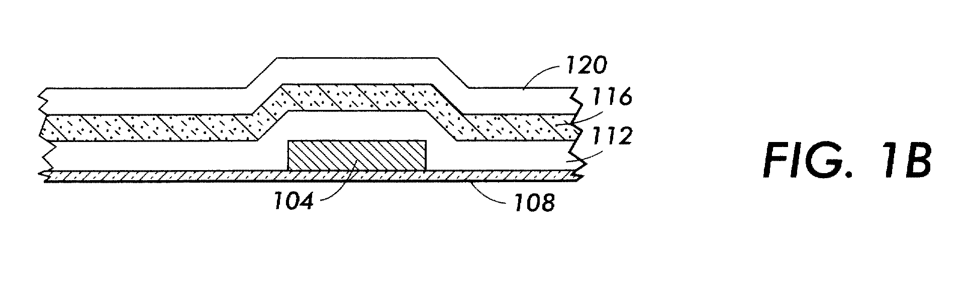
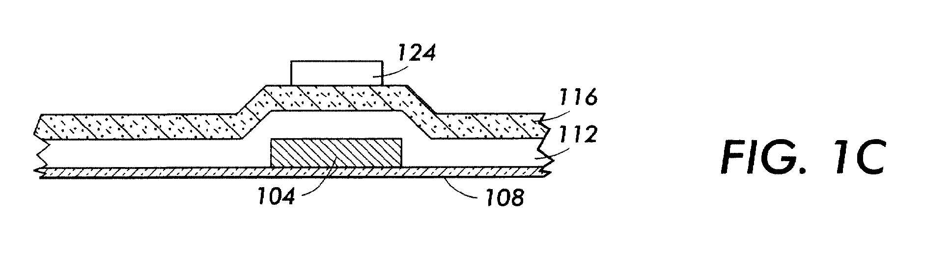
- Fig. 1 illustrates the fabrication of a thin film transistor (TFT) by laser doping portions of the TFT with a phosphorous nitride thin film.
- TFT thin film transistor
- a metal gate104 is deposited and patterned over a glass substrate 108.
- a deposition techniques such as plasma enhanced chemical vapor deposition (PECVD) is used to deposit a plurality of layers over the gate 104 and substrate 108.
- the layers include a nitride layer 112, an amorphous silicon layer 116 and a top passivation layer 120.
- top passivation layer 120 is a multilayer structure formed from alternating nitride and oxide multilayers.
- a backside exposure that uses metal gate 104 as a mask may be used to form an island 124 from the top passivation layer 120. Using a backside exposure simplifies the alignment of island 124 with gate 104.
- a doping region of amorphous silicon is doped.
- doping regions 129 are positioned on both sides of island 124.
- a DCC compound that includes at least one element from either from column III or column V of the periodic table is brought in close proximity to the amorphous silicon.
- Typical compounds may include the column III or column V element chemically bonded to form a nitride or oxide.
- a "compound” is defined as a combination of two or more elements that form a chemical bond. Thus a “compound” does not include mixtures or alloys in which the elements are not chemically bonded together. For example, water is defined as a compound whereas a mixture of hydrogen and oxygen is for purposes of this patent not considered a compound.
- phosphorous nitride One example of a compound that has been found to be suitable as a doping source is phosphorous nitride.
- the chemical bond between phosphor and nitride in the phosphor nitride compound makes the compound stable in air; phosphor itself is unstable in air.
- a first method of forming phosphorous nitride is to evaporate phosphor in a N 2 plasma.
- the evaporated phosphor deposits over the substrate as a phosphorous nitride film.
- a pulse discharge of a phosphorus powder covered electrode in a N 2 ambient gas may also be used to form a phosphorous nitride compound.
- Both techniques of generating a phosphorous nitride film are described in an article entitled "Solid Planar Diffusion Sources Based on Phosphorus Nitride Prepared by a One-stage Process in a Pulse Discharge" by M. Raicis and L. Raicis in Surface and Coatings Technology, Vol. 78, p. 238 (1996).
- An alternate method of bringing a DCC, including an element from column 3 or column 5 of the periodic table, into close proximity to amorphous silicon uses commercially available PECVD equipment.
- example parameters used to achieve PECVD deposition of a phosphorous nitride film 130 will be provided.
- a processing gas of one sccm (Standard cubic centimeter per minute) PH 5 and 100 sccm NH 3 is formed.
- Ten watts of 13.5MHz radio frequency power in a 400 mTorr ambient pressure converts the processing gas into a plasma.
- Exposing a substrate, such as glass substrate 108 at 250 degrees Centigrade, to the plasma results in a phosphorous nitride thin film with a reflection index of approximately 1.85.
- Using the provided example parameters results in a deposition rate of approximately 50 Angstroms per minute.
- a laser beam 132 irradiates the phosphorous nitride thin film to laser dope select regions of amorphous silicon 116.
- laser beam 132 originates from an excimer laser with a high fluence laser beam having a wavelength of 308nm. The laser beam briefly melts the amorphous silicon and decomposes the phosphorous thin film 128. The decomposing phosphorous thin film introduces phosphor atoms into the molten layer of amorphous silicon.
- Figure 2 is a graph that illustrates the sheet resistance of a doped amorphous silicon layer as a function of laser energy density used in laser doping. Each curve of the graph corresponds to a different dopant source. Curve 204 corresponds to a phosphorous nitride dopant source, curve 208 corresponds to a Psi alloy as a dopant source, curve 212 corresponds to a P+ implantation at a dosage of 3x10 15 cm -2 and curve 216 corresponds to a P+ implantation at a dosage of 1x10 15 cm -2 . The measurements were taken on a structure including a nitride and a 500 angstrom thick amorphous silicon layer deposited on a glass substrate.
- portions of the phosphorous nitride thin film to laser radiation may remain covered by the phosphorous nitride film.
- portions of phosphorous nitride films 128 deposited over passivation island 124 may not absorb or receive sufficient exposure to laser energy and thus may not be fully decomposed.
- Unexposed phosphorous nitride film has a very high resistivity. Therefore, in some TFT embodiments, the unexposed phosphorous nitride remains in the device without disturbing the self-aligned TFT operation.
- the high resistivity of phosphorus nitride allows its use as a gate dielectric material for InP MISFETS as described in an article entitled "Enhancement mode InP MISFET's with sulfide passivation and photo-CVD grown P3N5 gate insulators " by Y. Jeong, S. Jo, B. Lee and T. Sugano in the IEEE Electron Device Letters, Vol 16, Page 109 (1995)..
- a plasma cleaning process may be implemented.
- a small amount of CF4 typically 1 to 2 percent in O 2 , is used to remove the undesirable phosphorous nitride.
- metal source contact 136 and metal drain contact 140 are formed over the doped areas of amorphous silicon layer 116.
- a second passivation island 144 of SiO 2 may be formed between metal source contact 136 and metal drain contact 140.
- FIG. 4 A typical transfer characteristic curve of a TFT fabricated by the process described above is shown in Fig. 4.
- Figure 4 plots a normalized drain current as a function of an applied gate voltage. The performance is comparable to devices formed using dopant sources that are unstable in air such as structures described in the previously referenced patent by Mei et. al.
- Fig. 3 shows a system 300 for depositing phosphorous nitride using laser ablation.
- phosphorous nitride film 302 is deposited over a surface of a transparent source plate 304.
- the transparent source plate is positioned in close proximity to the semiconductor sample 306 with the phosphorous nitride film coated surface facing semiconductor sample 306.
- Gap 312 that separates the phosphorous nitride film 302 and semiconductor sample 306 is typically several microns, although the gap may range from zero to several millimeters.
- the height of spacers 308 determines the size of the gap. The smaller the gap between phosphorous nitride film 302 and semiconductor sample 306, the higher the dopant efficiency.
- a laser such as an excimer laser, outputs a laser beam that propagates through source plate 304 and irradiates a select area of phosphorous nitride film 302.
- the phosphorous nitride film absorbs a portion of the laser energy.
- a thin layer of opaque material such as a-Si, may be inserted between plate 304 and phosphorous nitride film 302 to enhance the efficiency of laser energy absorption.
- Absorbed energy from the laser pulse ablates phosphorous nitride film 302 causing phosphorous nitride film 302 to release energetic dopants into the gap between film 302 and semiconductor sample 306.
- the laser energy also melts a surface region of semiconductor sample 306. The depth of the melted region depends upon the laser energy and the pulse width (duration) as well as the thermal transport properties of the semiconductor (typically amorphous silicon) sample 306.
- a typical laser pulse width is approximately 50 nanoseconds.
- a PSi doping material is the suggested doping material.
- PSi doping material tends to break down when exposed to moisture in air.
- the stability in air of DCC compounds, such as phosphorous nitride, allows the dopant source plate to be prepared off line in a batch process and stored until needed for use.
Landscapes
- Thin Film Transistor (AREA)
- Crystals, And After-Treatments Of Crystals (AREA)
- Semiconductor Lasers (AREA)
Abstract

Description
- In recent years, laser doping has become a popular method for fabricating large area electronics. The low processing temperatures used in a laser doping process makes the process suitable for doping semiconductor layers on substrates that have low temperature tolerances. Examples of substrates with low temperature tolerances include plastic and glass.
- During laser doping, a laser pulse briefly melts a surface layer in a doping region of a semiconductor. While the doping region is in a molten state, a dopant source is introduced near a surface of the doping region. The dopant source provides dopant atoms that are distributed through the surface layer. After the doping region solidifies, the dopants are available for electrical activation.
- Typical dopant sources used to provide dopant atoms include: (1) gas dopant sources such as phosphorus fluoride (PF5) and boron fluoride (BF3), (2) spin-on dopants such as phosphorous doped silica solution, and (3) phosphor-silicon alloys which may be ablated from another substrate or deposited directly on the doping region.
- Each of the above described dopant sources has a corresponding disadvantage. For example, gas dopant sources are difficult to control and require the use of specialized equipment to prevent uneven distribution of dopants. Furthermore, both gas and spin-on deposition techniques have low doping efficiencies. A low doping efficiency makes it difficult to fabricate a heavily doped material. Phosphor-silicon alloy materials are difficult to deposit and unstable when exposed to moisture in air. In particular, moisture in the air decomposes the phosphor-silicon alloy. After decomposition, the moisture may redistribute the dopant atoms. Dopant atom redistribution produces high defect rates in devices formed from the doped semiconductor.
- Thus an improved method of laser doping is needed.
- Although laser doping has become a popular method of fabricating large area electronic devices, current laser dopant sources are difficult to control, require expensive equipment, or are unstable when exposed to moisture in the air. In order to avoid these problems, the invention describes a technique for using a thin film of dopant containing compound (DCC) as a laser doping source. The dopant containing compound (DCC) can be deposited by standard equipment and is stable in air. An example of a dopant containing compound is phosphorous nitride.
- In one embodiment of the invention, standard plasma enhanced chemical vapor deposition (PECVD) equipment is used to deposit a thin phosphorous nitride film over the dopant region. Alternatively, a transparent dopant plate may be used to position the phosphorous nitride near the dopant region in a laser ablation process. In laser ablation, a laser decomposes the phosphorous nitride. The laser also briefly melts the semiconductor in the dopant region to allow incorporation of dopant atoms into the doping region. After the doping process, remaining phosphor nitride may be removed using a plasma containing small amounts of CF4 diluted in oxygen.
- A particular embodiment in accordance with this invention will now be described with reference to the accompanying drawings; in which:-
- Fig. 1 illustrates a sequence of operations used to fabricate a Thin Film Transistor (TFT) structure using one embodiment of the invention;
- Fig. 2. is a graph illustrating the resistivity of laser doped amorphous silicon as a function of changing laser energies and dopant sources;
- Fig. 3 illustrates a system that uses laser ablation to provide dopant atoms from a film of phosphorous nitride to dope a semiconductor sample; and,
- Fig. 4 is a plot illustrating the TFT transfer characteristic of a device fabricated using a phosphorous nitride dopant.
-
- Fig. 1 illustrates the fabrication of a thin film transistor (TFT) by laser doping portions of the TFT with a phosphorous nitride thin film. Although the structure described is a TFT structure, it is understood that the described doping techniques are applicable to a large range of devices including other semiconductor active and passive devices such as resistors and transistors used in integrated circuits.
- In Fig. 1, a metal gate104 is deposited and patterned over a
glass substrate 108. A deposition techniques, such as plasma enhanced chemical vapor deposition (PECVD) is used to deposit a plurality of layers over thegate 104 andsubstrate 108. In the embodiment illustrated, the layers include anitride layer 112, anamorphous silicon layer 116 and atop passivation layer 120. In one embodiment of the invention,top passivation layer 120 is a multilayer structure formed from alternating nitride and oxide multilayers. A backside exposure that usesmetal gate 104 as a mask may be used to form anisland 124 from thetop passivation layer 120. Using a backside exposure simplifies the alignment ofisland 124 withgate 104. - After formation of
island 124, a doping region of amorphous silicon is doped. In the illustrated embodiment,doping regions 129 are positioned on both sides ofisland 124. To dope the amorphous silicon, a DCC compound that includes at least one element from either from column III or column V of the periodic table is brought in close proximity to the amorphous silicon. Typical compounds may include the column III or column V element chemically bonded to form a nitride or oxide. As used herein, a "compound" is defined as a combination of two or more elements that form a chemical bond. Thus a "compound" does not include mixtures or alloys in which the elements are not chemically bonded together. For example, water is defined as a compound whereas a mixture of hydrogen and oxygen is for purposes of this patent not considered a compound. - One example of a compound that has been found to be suitable as a doping source is phosphorous nitride. The chemical bond between phosphor and nitride in the phosphor nitride compound makes the compound stable in air; phosphor itself is unstable in air.
- A first method of forming phosphorous nitride is to evaporate phosphor in a N2 plasma. The evaporated phosphor deposits over the substrate as a phosphorous nitride film. Alternatively, a pulse discharge of a phosphorus powder covered electrode in a N2 ambient gas may also be used to form a phosphorous nitride compound. Both techniques of generating a phosphorous nitride film are described in an article entitled "Solid Planar Diffusion Sources Based on Phosphorus Nitride Prepared by a One-stage Process in a Pulse Discharge" by M. Raicis and L. Raicis in Surface and Coatings Technology, Vol. 78, p. 238 (1996).
- An alternate method of bringing a DCC, including an element from column 3 or
column 5 of the periodic table, into close proximity to amorphous silicon uses commercially available PECVD equipment. In the following description, example parameters used to achieve PECVD deposition of a phosphorous nitride film 130 will be provided. In the example, a processing gas of one sccm (Standard cubic centimeter per minute) PH5 and 100 sccm NH3 is formed. Ten watts of 13.5MHz radio frequency power in a 400 mTorr ambient pressure converts the processing gas into a plasma. Exposing a substrate, such asglass substrate 108 at 250 degrees Centigrade, to the plasma results in a phosphorous nitride thin film with a reflection index of approximately 1.85. Using the provided example parameters results in a deposition rate of approximately 50 Angstroms per minute. - After deposition, a
laser beam 132 irradiates the phosphorous nitride thin film to laser dope select regions ofamorphous silicon 116. In one embodiment,laser beam 132 originates from an excimer laser with a high fluence laser beam having a wavelength of 308nm. The laser beam briefly melts the amorphous silicon and decomposes the phosphorousthin film 128. The decomposing phosphorous thin film introduces phosphor atoms into the molten layer of amorphous silicon. - Figure 2 is a graph that illustrates the sheet resistance of a doped amorphous silicon layer as a function of laser energy density used in laser doping. Each curve of the graph corresponds to a different dopant source.
Curve 204 corresponds to a phosphorous nitride dopant source,curve 208 corresponds to a Psi alloy as a dopant source,curve 212 corresponds to a P+ implantation at a dosage of 3x1015 cm-2 andcurve 216 corresponds to a P+ implantation at a dosage of 1x1015 cm-2. The measurements were taken on a structure including a nitride and a 500 angstrom thick amorphous silicon layer deposited on a glass substrate. - To form the structure from which measurements were taken, 100 Angstroms of phosphorous nitride film was deposited over the amorphous silicon using the previously described example PECVD process. Pulses of laser light from a XeCl excimer laser decomposes the phosphorous nitride.
- After exposure to the excimer laser, a four point probe was used to measure the resistivity of the resulting doped amorphous silicon structure. At each laser energy density value plotted along a horizontal axis of Fig. 2, the phosphorous nitride dopant source plotted as
curve 204, produced the lowest resistance doped amorphous silicon. A low resistance demonstrates the high doping efficiency of the phosphorous nitride by indicating that almost all of the phosphorous nitride film decomposes under the laser exposure. - Returning to Fig. 1, after exposure of portions of the phosphorous nitride thin film to laser radiation, areas unexposed to laser radiation may remain covered by the phosphorous nitride film. In particular, during fabrication of laser-doped, self-aligned TFT structures, portions of
phosphorous nitride films 128 deposited overpassivation island 124 may not absorb or receive sufficient exposure to laser energy and thus may not be fully decomposed. Unexposed phosphorous nitride film has a very high resistivity. Therefore, in some TFT embodiments, the unexposed phosphorous nitride remains in the device without disturbing the self-aligned TFT operation. The high resistivity of phosphorus nitride allows its use as a gate dielectric material for InP MISFETS as described in an article entitled "Enhancement mode InP MISFET's with sulfide passivation and photo-CVD grown P3N5 gate insulators " by Y. Jeong, S. Jo, B. Lee and T. Sugano in the IEEE Electron Device Letters, Vol 16, Page 109 (1995).. - When complete removal of phosphorous nitride is desired, a plasma cleaning process may be implemented. In one implementation of such a plasma cleaning process, a small amount of CF4, typically 1 to 2 percent in O2, is used to remove the undesirable phosphorous nitride.
- After removal of undesired portions of phosphorous nitride thin film128,
metal source contact 136 andmetal drain contact 140 are formed over the doped areas ofamorphous silicon layer 116. To complete the TFT structure, asecond passivation island 144 of SiO2 may be formed betweenmetal source contact 136 andmetal drain contact 140. - A typical transfer characteristic curve of a TFT fabricated by the process described above is shown in Fig. 4. Figure 4 plots a normalized drain current as a function of an applied gate voltage. The performance is comparable to devices formed using dopant sources that are unstable in air such as structures described in the previously referenced patent by Mei et. al.
- Although the prior description has described using a PECVD technique to deposit the phosphorous nitride directly on a device for laser doping, it should be recognized that other techniques may be used to bring phosphorous nitride in close proximity to the device to be doped. For example, Fig. 3 shows a
system 300 for depositing phosphorous nitride using laser ablation. In Fig. 3,phosphorous nitride film 302 is deposited over a surface of atransparent source plate 304. The transparent source plate is positioned in close proximity to thesemiconductor sample 306 with the phosphorous nitride film coated surface facingsemiconductor sample 306.Gap 312 that separates thephosphorous nitride film 302 andsemiconductor sample 306 is typically several microns, although the gap may range from zero to several millimeters. The height ofspacers 308 determines the size of the gap. The smaller the gap betweenphosphorous nitride film 302 andsemiconductor sample 306, the higher the dopant efficiency. - After
phosphorous nitride film 302 is properly positioned over the semiconductor to be doped, a laser such as an excimer laser, outputs a laser beam that propagates throughsource plate 304 and irradiates a select area ofphosphorous nitride film 302. The phosphorous nitride film absorbs a portion of the laser energy. When the phosphorous nitride film absorption rate is too low, a thin layer of opaque material, such as a-Si, may be inserted betweenplate 304 andphosphorous nitride film 302 to enhance the efficiency of laser energy absorption. Absorbed energy from the laser pulse ablatesphosphorous nitride film 302 causingphosphorous nitride film 302 to release energetic dopants into the gap betweenfilm 302 andsemiconductor sample 306. In addition to ablatingphosphorous nitride film 302, the laser energy also melts a surface region ofsemiconductor sample 306. The depth of the melted region depends upon the laser energy and the pulse width (duration) as well as the thermal transport properties of the semiconductor (typically amorphous silicon)sample 306. A typical laser pulse width is approximately 50 nanoseconds. After receiving the laser pulse, the semiconductor remains in a molten state for a short time interval allowingsemiconductor sample 306 to incorporate some of the dopant atoms released in the gap during the laser ablation process. The absorbed dopants are activated whensemiconductor sample 306 solidifies. A more detailed description of using laser ablation is described in U.S. Patent 5,871,826 (the '826 reference) entitled Proximity Laser Doping Technique for Electronic Materials by inventors Ping Mei, Rene A. Lujan and James B. Boyce which is hereby incorporated by reference. - In the '826 reference, a PSi doping material is the suggested doping material. However, PSi doping material tends to break down when exposed to moisture in air. The stability in air of DCC compounds, such as phosphorous nitride, allows the dopant source plate to be prepared off line in a batch process and stored until needed for use.
Claims (10)
- A method of doping a semiconductor comprising the operations of:placing a layer of a dopant containing compound that is stable in air in close proximity to a semiconductor surface; anddirecting a laser to dope the semiconductor with atoms from the layer of dopant containing compound.
- A method according to claim 1, wherein the dopant containing compound is formed from a nitride and at least one element from a group of column three or column five of the periodic table.
- A method according to claim 1 or 2, wherein the dopant containing compound is phosphorous nitride.
- A method according to any one of the preceding claims, wherein the operation of placing the layer of dopant containing compound in close proximity to the semiconductor surface includes:
depositing the dopant containing compound on the semiconductor surface using plasma enhanced chemical vapor deposition. - A method according to claim 4, wherein the operation of placing the layer of dopant containing compound in close proximity to the semiconductor surface includes:depositing the dopant containing compound on a transparent surface; andpositioning the dopant containing compound over the semiconductor surface to allow a laser beam from the laser to pass through the transparent surface and cause atoms from the dopant containing compound to dope the semiconductor.
- A method according to claim 3 or 4, wherein a laser beam from the laser:decomposes the dopant containing compound; and,melts the semiconductor.
- A method of doping a semiconductor material with a donor material comprising the operations of:providing a source plate;providing a layer of phosphorous nitride on one side of the source plate;
placing the source place in close proximity with the semiconductor material with the one side facing the semiconductor material;irradiating the phosphorous nitride with a laser source passing through the source plate, the irradiation resulting in ablating the phosphorous nitride layer and melting a region of the semiconductor material; andintroducing atoms from the phosphorous nitride into the region of the semiconductor material. - A method according to claim 7, further comprising the operation of:
providing an absorption layer between the source plate and the phosphorous nitride layer. - A method according to claim 7 or 8, wherein the semiconductor material is amorphous silicon; the region of the amorphous silicon having a sheet resistivity below 1000 ohms per square.
- A structure to be used in the formation of a thin film transistor comprising:a substrate;a gate deposited over the substrate;a semiconductor layer formed over the substrate and the gate; anda phosphorous nitride film formed adjacent to the semiconductor layer, the phosphorous nitride film decomposed and used to dope the semiconductor layer.
Applications Claiming Priority (2)
| Application Number | Priority Date | Filing Date | Title |
|---|---|---|---|
| US473576 | 1999-12-28 | ||
| US09/473,576 US6586318B1 (en) | 1999-12-28 | 1999-12-28 | Thin phosphorus nitride film as an N-type doping source used in laser doping technology |
Publications (3)
| Publication Number | Publication Date |
|---|---|
| EP1113486A2 true EP1113486A2 (en) | 2001-07-04 |
| EP1113486A3 EP1113486A3 (en) | 2001-09-26 |
| EP1113486B1 EP1113486B1 (en) | 2010-12-01 |
Family
ID=23880132
Family Applications (1)
| Application Number | Title | Priority Date | Filing Date |
|---|---|---|---|
| EP00311109A Expired - Lifetime EP1113486B1 (en) | 1999-12-28 | 2000-12-13 | Method of doping a semiconductor |
Country Status (4)
| Country | Link |
|---|---|
| US (2) | US6586318B1 (en) |
| EP (1) | EP1113486B1 (en) |
| JP (1) | JP2001223174A (en) |
| DE (1) | DE60045302D1 (en) |
Families Citing this family (28)
| Publication number | Priority date | Publication date | Assignee | Title |
|---|---|---|---|---|
| US6586318B1 (en) * | 1999-12-28 | 2003-07-01 | Xerox Corporation | Thin phosphorus nitride film as an N-type doping source used in laser doping technology |
| US7057256B2 (en) | 2001-05-25 | 2006-06-06 | President & Fellows Of Harvard College | Silicon-based visible and near-infrared optoelectric devices |
| US7442629B2 (en) | 2004-09-24 | 2008-10-28 | President & Fellows Of Harvard College | Femtosecond laser-induced formation of submicrometer spikes on a semiconductor substrate |
| JP4387091B2 (en) * | 2002-11-05 | 2009-12-16 | 株式会社半導体エネルギー研究所 | Method for manufacturing thin film transistor |
| TWI280667B (en) * | 2006-04-11 | 2007-05-01 | Au Optronics Corp | A manufacturing method for a liquid crystal display |
| US7501648B2 (en) * | 2006-08-16 | 2009-03-10 | International Business Machines Corporation | Phase change materials and associated memory devices |
| JP4625793B2 (en) * | 2006-09-08 | 2011-02-02 | 株式会社東芝 | Semiconductor device |
| KR101369993B1 (en) * | 2006-12-18 | 2014-03-06 | 어플라이드 머티어리얼스, 인코포레이티드 | Safe handling of low energy, high dose arsenic, phosphorus, and boron implanted wafers |
| KR101329352B1 (en) * | 2007-10-17 | 2013-11-13 | 삼성전자주식회사 | Method for manufacturing of semiconductor device |
| US7989329B2 (en) * | 2007-12-21 | 2011-08-02 | Applied Materials, Inc. | Removal of surface dopants from a substrate |
| US8207051B2 (en) * | 2009-04-28 | 2012-06-26 | Sionyx, Inc. | Semiconductor surface modification |
| US7799666B1 (en) | 2009-07-27 | 2010-09-21 | Potomac Photonics, Inc. | Method of spatially selective laser-assisted doping of a semiconductor |
| US9673243B2 (en) | 2009-09-17 | 2017-06-06 | Sionyx, Llc | Photosensitive imaging devices and associated methods |
| US9911781B2 (en) | 2009-09-17 | 2018-03-06 | Sionyx, Llc | Photosensitive imaging devices and associated methods |
| US8692198B2 (en) | 2010-04-21 | 2014-04-08 | Sionyx, Inc. | Photosensitive imaging devices and associated methods |
| CN103081128B (en) | 2010-06-18 | 2016-11-02 | 西奥尼克斯公司 | High-speed photosensitive device and related method |
| US8580664B2 (en) | 2011-03-31 | 2013-11-12 | Tokyo Electron Limited | Method for forming ultra-shallow boron doping regions by solid phase diffusion |
| US8569158B2 (en) * | 2011-03-31 | 2013-10-29 | Tokyo Electron Limited | Method for forming ultra-shallow doping regions by solid phase diffusion |
| US9496308B2 (en) | 2011-06-09 | 2016-11-15 | Sionyx, Llc | Process module for increasing the response of backside illuminated photosensitive imagers and associated methods |
| JP2014525091A (en) | 2011-07-13 | 2014-09-25 | サイオニクス、インク. | Biological imaging apparatus and related method |
| JP6239227B2 (en) * | 2011-11-30 | 2017-11-29 | 株式会社半導体エネルギー研究所 | Semiconductor device and manufacturing method of semiconductor device |
| US9064764B2 (en) | 2012-03-22 | 2015-06-23 | Sionyx, Inc. | Pixel isolation elements, devices, and associated methods |
| TWI476933B (en) * | 2012-03-27 | 2015-03-11 | 鴻海精密工業股份有限公司 | Thin film transistor |
| WO2014127376A2 (en) | 2013-02-15 | 2014-08-21 | Sionyx, Inc. | High dynamic range cmos image sensor having anti-blooming properties and associated methods |
| US9939251B2 (en) | 2013-03-15 | 2018-04-10 | Sionyx, Llc | Three dimensional imaging utilizing stacked imager devices and associated methods |
| WO2014209421A1 (en) | 2013-06-29 | 2014-12-31 | Sionyx, Inc. | Shallow trench textured regions and associated methods |
| US9899224B2 (en) | 2015-03-03 | 2018-02-20 | Tokyo Electron Limited | Method of controlling solid phase diffusion of boron dopants to form ultra-shallow doping regions |
| CN115084275B (en) | 2021-03-15 | 2024-09-27 | 京东方科技集团股份有限公司 | Metal oxide TFT and manufacturing method, X-ray detector and display panel |
Citations (1)
| Publication number | Priority date | Publication date | Assignee | Title |
|---|---|---|---|---|
| US5871826A (en) | 1996-05-30 | 1999-02-16 | Xerox Corporation | Proximity laser doping technique for electronic materials |
Family Cites Families (17)
| Publication number | Priority date | Publication date | Assignee | Title |
|---|---|---|---|---|
| US4415526A (en) * | 1977-05-31 | 1983-11-15 | Metco Properties | Metal phthalocyanine on a substrate |
| US4276557A (en) * | 1978-12-29 | 1981-06-30 | Bell Telephone Laboratories, Incorporated | Integrated semiconductor circuit structure and method for making it |
| US4737429A (en) * | 1986-06-26 | 1988-04-12 | Xerox Corporation | Layered amorphous silicon imaging members |
| JP2819694B2 (en) * | 1989-11-17 | 1998-10-30 | 富士ゼロックス株式会社 | Method for manufacturing MOS type semiconductor device |
| JPH04269832A (en) * | 1991-02-26 | 1992-09-25 | Shin Etsu Chem Co Ltd | Method for manufacturing a mask for X-ray lithography |
| JPH07135308A (en) * | 1993-11-10 | 1995-05-23 | Fujitsu Ltd | Method for manufacturing semiconductor device |
| JPH10144633A (en) * | 1996-11-08 | 1998-05-29 | Mitsubishi Electric Corp | Method for manufacturing semiconductor device |
| US5908307A (en) * | 1997-01-31 | 1999-06-01 | Ultratech Stepper, Inc. | Fabrication method for reduced-dimension FET devices |
| US5885904A (en) * | 1997-02-14 | 1999-03-23 | Advanced Micro Devices, Inc. | Method to incorporate, and a device having, oxide enhancement dopants using gas immersion laser doping (GILD) for selectively growing an oxide layer |
| US5904575A (en) * | 1997-02-14 | 1999-05-18 | Advanced Micro Devices, Inc. | Method and apparatus incorporating nitrogen selectively for differential oxide growth |
| US5918140A (en) | 1997-06-16 | 1999-06-29 | The Regents Of The University Of California | Deposition of dopant impurities and pulsed energy drive-in |
| CA2211949A1 (en) * | 1997-07-21 | 1999-01-29 | David Farley Johnson | Nonaqueous compositions for parenteral administration |
| US6107641A (en) * | 1997-09-10 | 2000-08-22 | Xerox Corporation | Thin film transistor with reduced parasitic capacitance and reduced feed-through voltage |
| JPH11298090A (en) * | 1998-04-09 | 1999-10-29 | Nichia Chem Ind Ltd | Nitride semiconductor device |
| US5956603A (en) * | 1998-08-27 | 1999-09-21 | Ultratech Stepper, Inc. | Gas immersion laser annealing method suitable for use in the fabrication of reduced-dimension integrated circuits |
| KR100281692B1 (en) * | 1998-10-17 | 2001-03-02 | 윤종용 | Self-aligned contact pad of semiconductor device and method of forming the same |
| US6586318B1 (en) * | 1999-12-28 | 2003-07-01 | Xerox Corporation | Thin phosphorus nitride film as an N-type doping source used in laser doping technology |
-
1999
- 1999-12-28 US US09/473,576 patent/US6586318B1/en not_active Expired - Lifetime
-
2000
- 2000-12-13 EP EP00311109A patent/EP1113486B1/en not_active Expired - Lifetime
- 2000-12-13 DE DE60045302T patent/DE60045302D1/en not_active Expired - Lifetime
- 2000-12-14 JP JP2000379598A patent/JP2001223174A/en active Pending
-
2002
- 2002-10-28 US US10/282,265 patent/US6818535B2/en not_active Expired - Lifetime
Patent Citations (1)
| Publication number | Priority date | Publication date | Assignee | Title |
|---|---|---|---|---|
| US5871826A (en) | 1996-05-30 | 1999-02-16 | Xerox Corporation | Proximity laser doping technique for electronic materials |
Non-Patent Citations (3)
| Title |
|---|
| FORGARASSY, E. ET AL.: "Pulsed laser crystallization and doping for the fabrication of high-quality poly-Si TFTs", APPLIED SURFACE SCIENCE, vol. 69, 1993, pages 231 - 241 |
| M. RAICIS; L. RAICIS: "Solid Planar Diffusion Sources Based on Phosphorus Nitride Prepared by a One-stage Process in a Pulse Discharge", SURFACE AND COATINGS TECHNOLOGY, vol. 78, 1996, pages 238 |
| Y. JEONG ET AL.: "Enhancement mode InP MISFET's with sulfide passivation and photo-CVD grown P3N5 gate insulators", IEEE ELECTRON DEVICE LETTERS, vol. 16, 1995, pages 109 |
Also Published As
| Publication number | Publication date |
|---|---|
| US6818535B2 (en) | 2004-11-16 |
| US6586318B1 (en) | 2003-07-01 |
| JP2001223174A (en) | 2001-08-17 |
| DE60045302D1 (en) | 2011-01-13 |
| EP1113486B1 (en) | 2010-12-01 |
| US20030067037A1 (en) | 2003-04-10 |
| EP1113486A3 (en) | 2001-09-26 |
Similar Documents
| Publication | Publication Date | Title |
|---|---|---|
| EP1113486B1 (en) | Method of doping a semiconductor | |
| Lee et al. | Thin film MOSFET’s fabricated in laser‐annealed polycrystalline silicon | |
| JP4387091B2 (en) | Method for manufacturing thin film transistor | |
| JP4166298B2 (en) | Method of introducing chemical elements into receiving materials | |
| US7517709B1 (en) | Method of forming backside point contact structures for silicon solar cells | |
| JP4295922B2 (en) | Gas immersion laser annealing method suitable for application in the fabrication of small integrated circuits | |
| KR100879494B1 (en) | Method of doping a semiconductor gate | |
| KR100285796B1 (en) | Semiconductor device manufacturing method and semiconductor device | |
| JP3869189B2 (en) | Method for manufacturing thin film transistor | |
| US6573161B1 (en) | Thin film semiconductor device fabrication process | |
| EP0036137A1 (en) | Method for production of semiconductor devices | |
| US20090149007A1 (en) | Electronic device and method of manufacturing the same | |
| IE51992B1 (en) | Method for manufacturing a semiconductor device | |
| US6348367B1 (en) | Method for manufacturing a semiconductor device | |
| WO2004090195A1 (en) | Crystalline-si-layer-bearing substrate and its production method, and crystalline si device | |
| KR19990044046A (en) | Method of manufacturing electronic device with thin film transistor | |
| US4651182A (en) | Insulated-gate field effect transistor and method of fabricating the same | |
| JPH05160153A (en) | Manufacture of semiconductor device | |
| KR101169058B1 (en) | Thin film transistor and fabrication method of the same | |
| JPS6235571A (en) | Manufacture of semiconductor device | |
| EP0084985A2 (en) | Laser induced flow Ge-O based materials | |
| Sameshima et al. | Fabrication of heavily-doped polycrystalline silicon film using a laser-doping technique | |
| EP0641018A1 (en) | Manufacturing method of semiconductor device and thin film transistor with a recrystallized thin semiconductor film | |
| US7517740B2 (en) | Method of crystallizing/activating polysilicon layer and method of fabricating thin film transistor having the same polysilicon layer | |
| US6798023B1 (en) | Semiconductor device comprising first insulating film, second insulating film comprising organic resin on the first insulating film, and pixel electrode over the second insulating film |
Legal Events
| Date | Code | Title | Description |
|---|---|---|---|
| PUAI | Public reference made under article 153(3) epc to a published international application that has entered the european phase |
Free format text: ORIGINAL CODE: 0009012 |
|
| AK | Designated contracting states |
Kind code of ref document: A2 Designated state(s): AT BE CH CY DE DK ES FI FR GB GR IE IT LI LU MC NL PT SE TR Kind code of ref document: A2 Designated state(s): DE FR GB |
|
| AX | Request for extension of the european patent |
Free format text: AL;LT;LV;MK;RO;SI |
|
| PUAL | Search report despatched |
Free format text: ORIGINAL CODE: 0009013 |
|
| RIC1 | Information provided on ipc code assigned before grant |
Free format text: 7H 01L 21/225 A, 7H 01L 29/786 B, 7H 01L 21/336 B |
|
| AK | Designated contracting states |
Kind code of ref document: A3 Designated state(s): AT BE CH CY DE DK ES FI FR GB GR IE IT LI LU MC NL PT SE TR |
|
| AX | Request for extension of the european patent |
Free format text: AL;LT;LV;MK;RO;SI |
|
| 17P | Request for examination filed |
Effective date: 20020326 |
|
| AKX | Designation fees paid |
Free format text: DE FR GB |
|
| 17Q | First examination report despatched |
Effective date: 20070716 |
|
| R17C | First examination report despatched (corrected) |
Effective date: 20070910 |
|
| GRAP | Despatch of communication of intention to grant a patent |
Free format text: ORIGINAL CODE: EPIDOSNIGR1 |
|
| GRAS | Grant fee paid |
Free format text: ORIGINAL CODE: EPIDOSNIGR3 |
|
| GRAA | (expected) grant |
Free format text: ORIGINAL CODE: 0009210 |
|
| AK | Designated contracting states |
Kind code of ref document: B1 Designated state(s): DE FR GB |
|
| REG | Reference to a national code |
Ref country code: GB Ref legal event code: FG4D |
|
| REF | Corresponds to: |
Ref document number: 60045302 Country of ref document: DE Date of ref document: 20110113 Kind code of ref document: P |
|
| PLBE | No opposition filed within time limit |
Free format text: ORIGINAL CODE: 0009261 |
|
| STAA | Information on the status of an ep patent application or granted ep patent |
Free format text: STATUS: NO OPPOSITION FILED WITHIN TIME LIMIT |
|
| 26N | No opposition filed |
Effective date: 20110902 |
|
| REG | Reference to a national code |
Ref country code: DE Ref legal event code: R097 Ref document number: 60045302 Country of ref document: DE Effective date: 20110902 |
|
| REG | Reference to a national code |
Ref country code: FR Ref legal event code: PLFP Year of fee payment: 16 |
|
| REG | Reference to a national code |
Ref country code: FR Ref legal event code: PLFP Year of fee payment: 17 |
|
| REG | Reference to a national code |
Ref country code: FR Ref legal event code: PLFP Year of fee payment: 18 |
|
| PGFP | Annual fee paid to national office [announced via postgrant information from national office to epo] |
Ref country code: FR Payment date: 20171121 Year of fee payment: 18 Ref country code: DE Payment date: 20171120 Year of fee payment: 18 |
|
| PGFP | Annual fee paid to national office [announced via postgrant information from national office to epo] |
Ref country code: GB Payment date: 20171121 Year of fee payment: 18 |
|
| REG | Reference to a national code |
Ref country code: DE Ref legal event code: R119 Ref document number: 60045302 Country of ref document: DE |
|
| GBPC | Gb: european patent ceased through non-payment of renewal fee |
Effective date: 20181213 |
|
| PG25 | Lapsed in a contracting state [announced via postgrant information from national office to epo] |
Ref country code: FR Free format text: LAPSE BECAUSE OF NON-PAYMENT OF DUE FEES Effective date: 20181231 Ref country code: DE Free format text: LAPSE BECAUSE OF NON-PAYMENT OF DUE FEES Effective date: 20190702 |
|
| PG25 | Lapsed in a contracting state [announced via postgrant information from national office to epo] |
Ref country code: GB Free format text: LAPSE BECAUSE OF NON-PAYMENT OF DUE FEES Effective date: 20181213 |