EP1113462A2 - Method and apparatus for transmitting fibre-channel and non-fibre channel signals through common cable. - Google Patents
Method and apparatus for transmitting fibre-channel and non-fibre channel signals through common cable. Download PDFInfo
- Publication number
- EP1113462A2 EP1113462A2 EP00311748A EP00311748A EP1113462A2 EP 1113462 A2 EP1113462 A2 EP 1113462A2 EP 00311748 A EP00311748 A EP 00311748A EP 00311748 A EP00311748 A EP 00311748A EP 1113462 A2 EP1113462 A2 EP 1113462A2
- Authority
- EP
- European Patent Office
- Prior art keywords
- port
- fibre channel
- director
- pass
- disk drives
- Prior art date
- Legal status (The legal status is an assumption and is not a legal conclusion. Google has not performed a legal analysis and makes no representation as to the accuracy of the status listed.)
- Granted
Links
- 239000000835 fiber Substances 0.000 title claims abstract description 88
- 238000000034 method Methods 0.000 title claims abstract description 16
- 239000004020 conductor Substances 0.000 claims abstract description 30
- 230000015654 memory Effects 0.000 description 32
- 238000012360 testing method Methods 0.000 description 18
- 238000010586 diagram Methods 0.000 description 11
- 238000013500 data storage Methods 0.000 description 9
- 230000005540 biological transmission Effects 0.000 description 8
- 238000010168 coupling process Methods 0.000 description 8
- 238000005859 coupling reaction Methods 0.000 description 8
- 238000004891 communication Methods 0.000 description 7
- 230000004044 response Effects 0.000 description 7
- 238000010276 construction Methods 0.000 description 6
- 230000008878 coupling Effects 0.000 description 6
- 238000012546 transfer Methods 0.000 description 5
- 230000009471 action Effects 0.000 description 4
- 230000008569 process Effects 0.000 description 4
- 239000012858 resilient material Substances 0.000 description 4
- 238000001514 detection method Methods 0.000 description 2
- 230000000694 effects Effects 0.000 description 2
- 230000009977 dual effect Effects 0.000 description 1
- 230000006870 function Effects 0.000 description 1
- 230000007257 malfunction Effects 0.000 description 1
- 239000000463 material Substances 0.000 description 1
- 230000013011 mating Effects 0.000 description 1
- 230000007246 mechanism Effects 0.000 description 1
- 238000012545 processing Methods 0.000 description 1
- 239000011359 shock absorbing material Substances 0.000 description 1
- 238000010998 test method Methods 0.000 description 1
- 230000007704 transition Effects 0.000 description 1
Images














Classifications
-
- H—ELECTRICITY
- H01—ELECTRIC ELEMENTS
- H01B—CABLES; CONDUCTORS; INSULATORS; SELECTION OF MATERIALS FOR THEIR CONDUCTIVE, INSULATING OR DIELECTRIC PROPERTIES
- H01B11/00—Communication cables or conductors
- H01B11/22—Cables including at least one electrical conductor together with optical fibres
Definitions
- This invention relates generally to data storage systems and more particularly to data storage systems having a plurality of magnetic storage disk drives in a redundancy arrangement whereby the disk drives are controllable by first disk controllers and second disk controllers. Still more particularly, the invention also relates to systems of such type wherein the disk drives are coupled to the disk controllers through a series, unidirectional, "ring" or, fiber channel protocol, communication system.
- each set is controlled by a first disk controller and a second disk controller. More particularly, in order to enable the set of disk drives to operate in the event that there is a failure of the first disk controller, each set is also coupled to a second, or redundant disk controller. Therefore, if either the first or second disk controller fails, the set of disk drives is accessible by the other one of the disk controllers.
- FC fibre channel
- ring a separate, independent, "ring”, or fibre channel communication protocol.
- two fibre channels are provided for each set of disk drives and their disk interfaces; a first fibre channel and a second fibre channel.
- the first fibre channel becomes "broken", or open, and becomes inoperative.
- the data stored in the entire portion of the set of disk drives coupled to the first disk channel is therefore unavailable until the inoperative first disk controller or inoperative disk drive is replaced. This is true with either the first channel or the second channel.
- a switch sometimes referred to as an LRC (i.e., a loop resiliency circuit) switch.
- LRC switch is used to remove an inoperative disk drive from its channel.
- a printed circuit board is provided for each disk drive.
- the printed circuit board has a pair of LRCs, one for the first channel and one for the second channel.
- the open channel may be "closed" in the event of an inoperative disk drive by placing the LRC thereof in a by-pass condition. While such suggested technique solves the inoperative disk drive, or open channel problem, if one of the pair of LRCs fails, the entire printed circuit board having the pair of LRCs must be replaced thereby disrupting both the first and second channels; and, hence, disrupting the operation of the entire data storage system.
- n LRC switches (where n is the number of disk drives in the set) in the first channel, i.e., one LRC for each one the n disk drives in the set and another n LRC switches in the second channel for each one of the n disk drives in the second channel.
- the first channel set of n LRCs is mounted on one printed circuit board and the second channel set of n LRCs is mounted on a different printed circuit board.
- a backplane is used to interconnect the two LRC printed circuit boards, the associated selectors, or multiplexers, and the disk drives. In order to provide the requisite serial, or sequential, fibre channel connections, an elaborate, complex, fan-out wiring arrangement has been suggested for the backplane.
- a method for transmitting fibre channel signals and non-fibre channel signals.
- the method includes: providing a cable having a connector at each end thereof; and transmitting both the fibre-channel signals and the non-fibre channel signals through the cable between the connectors.
- the non- fibre channel signals are transmitted in outer region of the cable and the fibre channel signals are transmitted in a region of the cable interior to the outer region.
- a cable in accordance with another feature of the invention, has a pair of connectors each one having a plurality of pins.
- the cable includes a first plurality of conductors arrange to transmit fibre channel signals. Ends of such conductors are connected to pins in each one of the pair of connectors.
- a second plurality of conductors is disposed around the first plurality of conductors. Ends of such conductors are connected to pins in each one of the pair of connectors.
- the cable includes a conductive shield disposed between the first plurality of conductors and the second plurality of conductors.
- the cable includes a second conductive shield disposed about both the first and second pluralities of conductors.
- a data storage system 10 is shown wherein a host computer 12 is coupled to a bank 14 of disk drives through a system interface 16.
- the system interface 16 includes a cache memory 18, having a high memory address section 18H and a low address memory section 18L.
- a plurality of directors 20 0 -20 15 is provided for controlling data transfer between the host computer 12 and the bank 14 of disk drives as such data passes through the cache memory 18.
- a pair of high address busses TH, BH is electrically connected to the high address memory section 18H.
- a pair of low address busses TL, BL is electrically connected to the low address memory section 18L.
- the cache memory 18 has a plurality of storage location addresses.
- each one of the directors 20 0 -20 15 is electrically connected to one of the pair of high address busses TH, BH and one of the pair of low address busses TL, BL.
- each one of the directors 20 0 -20 15 is able to address all locations in the entire cache memory 18 (i.e., to both the high address memory sections 18H and the low address memory sections 18L) and is therefore able to store data in and retrieve data from any storage location in the entire cache memory 18.
- a rear-end portion of the directors here directors 20 0 -20 3 and 20 12 -20 15 , is electrically connected to the bank 14 of disk drives through I/O adapter cards 22 0 -22 3 and 22 12 B22 15 , respectively and fibre channel (FC) port by-pass sections 23 1 -23 8 (described in more detail in connection with FIG. 2), respectively.
- a front-end portion of the directors, here directors 20 4 -20 11 is electrically connected to the host computer 12 through I/O adapter cards 22 1 -22 8 , respectively, as indicated.
- each end of the busses TH, TL, BH, BL terminates in a pair of master and slave arbiters bus arbiters, not shown, as described in co-pending patent application Serial No. 09/224,194 filed December 30, 1998, entitled DATA STORAGE SYSTEM, inventor Mark Zani, assigned to the same assignee as the present invention, the entire subject matter thereof being incorporated herein by reference.
- the host computer 12 issues a write request to one of the front-end directors 20 4 -20 11 to perform a write command.
- One of the front-end directors 20 4 -20 11 replies to the request and asks the host computer 12 for the data.
- the director determines the size of the data and reserves space in the cache memory 18 to store the request.
- the front-end director then produces control signals on either a high address memory bus (TH or BH) or a low memory address bus (TL, BL) connected to such front-end director depending on the location in the cache memory 18 allocated to store the data and enable the transfer to the cache memory 18.
- TH or BH high address memory bus
- TL, BL low memory address bus
- the host computer 12 then transfers the data to the front-end director.
- the front-end director then advises the host computer 12 that the transfer is complete.
- the front-end director looks up in a Table, not shown, stored in the cache memory 18 to determine which one of the rear-end directors 20 0 -20 3 and 20 12 -20 15 is to handle this request.
- the Table maps the host computer 12 address into an address in the bank 14 of disk drives.
- the front-end director then puts a notification in a "mail box" (not shown and stored in the cache memory 18) for the rear-end director which is to handle the request, the amount of the data and the disk address for the data.
- Other rear-end directors poll the cache memory 18 when they are idle to check their "mail boxes".
- the rear-end director processes the request, addresses the disk drive in the bank, reads the data from the cache memory and writes it into the addresses of a disk drive in the bank 14.
- the system operates in a reciprocal manner.
- Each one of the rear-end portion of the directors 20 0 -20 3 and 20 12 -20 15 is identical in construction and are described in detail in the above-referenced co-pending patent application Serial No. 09/224,194 to include a pair of central processing sections, CPU X and CPU Y, a dual port random access memory (RAM), and shared resources (Flash memories, etc,) coupled to the bank 14 of disk drives (FIG. 1) through the I/O adapter cards 20 0 -20 3 and 20 12 -20 15 and the fibre channel (FC) port by-pass sections 23 1 -23 8 as indicated and to a high memory address bus, here TH, and low memory address bus, here BL.
- TH high memory address bus
- BL low memory address bus
- each one of the directors 20 0 -20 3 and 20 12 -20 15 has a first output port, A, and a second output port, B.
- different pairs of the rear-end directors 20 0 , 20 1 ; 20 2 , 20 3 ; 20 12 , 20 13 (not shown); and, 20 14 , 20 15 are arranged in redundant fibre channel (FC) networks 25 1 -25 4 , respectively, as indicated.
- each one of the redundant fibre channel (FC) networks 25 1 -25 4 also includes: pairs of the I/O adapter cards 22 0 , 22 1 : 22 2 .
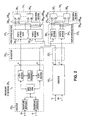
- Each one of the pairs of the redundant fibre channel (FC) networks 25 1 -25 4 is identical in construction, an exemplary one thereof, here redundant fibre channel (FC) networks 25 1 is shown in detail in FIG. 2. As noted from FIG. 2,
- director 20 0 is connected to busses TH and BL and that director 20 1 is connected to busses TL and BH.
- the redundant FC network 25 1 (FIG. 1) is also coupled, via directors 20 0 and 20 1 to all four busses TH, BH, TL, and BL.
- redundant FC network 25 1 For an exemplary one of the redundant FC networks 25 1 -25 4 , here redundant FC network 25 1 , it is noted that the first port A and second port B of director 20 0 are connected, through I/O adapter 22 0 , to FC port by-pass section 23 1 and to FC port by-pass section 23 2 , respectively. Likewise, the first port A and second port B of director 20 1 are connected, through I/O adapter 22 1 , to FC port by-pass section 23 1 and to FC port by-pass section 23 2 , respectively.
- Each one of the FC port by-pass sections 23 1 , 23 2 includes a pair of FC port by-pass cards 34 1 and 34 2 ; here, an A port by-pass card 34 1 and a B port by-pass card 34 2 .
- Each one of the disk drive sections 14 1- 14 8 (FIG. 1) includes a plurality of, here eight, disk drives, 36 1 -36 8 , as indicated for disk drive sections 14 1 and 14 2 in FIG. 2, it being understood that the number of disk drives in a section can be selected in accordance with the requisite storage requirements.
- Each one of the disk drives 36 1 -36 8 has a pair of redundant ports, i.e., a Port A and a Port B, as shown. Further, the A port by-pass card 34 1 , of each one of the port by-pass sections 23 1 , 23 2 is connected to the A ports of the disk drives 36 1 -36 8 in a corresponding one of the disk drive sections 14 1 , 14 2 , respectively, as shown.
- the port A by-pass card 34 1 of port by-pass section 23 1 is connected to the A port of the disk drives 36 1 -36 8 in disk drive section 14 1 and the port A by-pass card 34 1 of port by-pass section 23 2 is connected to the A port of the disk drives 36 1 -36 8 in disk drive section 14 2 , as shown.
- the B port by-pass card 34 2 , of each one of the port by-pass sections 23 1 , 23 2 is connected to the B ports of the disk drives 36 1 -36 8 in a corresponding one of the disk drive sections 14 1 , 14 2 , respectively, as shown.
- the port B by-pass card 34 2 of port by-pass section 23 1 is connected to the B port of the disk drives 36 1 -36 8 in disk drive section 14 1 and the port B by-pass card 34 2 of port by-pass section 23 2 is connected to the B port of the disk drives 36 1 -36 8 in disk drive section 14 2 , as shown.
- port B by-pass card 34 2 of port by-pass section 23 1 is also shown in FIG. 3 connected between the B ports of the disk drives 36 1 -36 8 in set 14 1 of disk drives and the I/O adapter 22 1 -director 20 1 .
- director 20 0 is able to access the disk drives 36 1 -36 8 in set 14 2 through its port B and, likewise, in the event of a failure in director 20 0 director 20 1 is able to access disk drives 36 1 -36 8 in set 14 1 through its A port. It is also noted that in the event of a failure of, or removal of, any one of the port A or port B by-pass cards 34 1 , 34 2 , both sets of disk drives 14 1 and 14 2 are still accessible from one of the directors 20 0 and 20 1 .
- the set 14 1 of disk drives is accessible from director 20 1 , via the path between port A of director 20 1 , the port B by-pass card 34 2 of fibre channel by-pass section 23 1 , and the port B of the disk drives in set 14 1 .
- the set 14 1 of disk drives is accessible from director 20 0 , via the path between port A of director 20 0 , the port A by-pass 34 1 of fibre channel by-pass section 23 1 , and the port A of the disk drives in set 14 1 .
- the set 14 2 of disk drives is accessible from director 20 1 , via the path between port B of director 20 1 , the port B by-pass card 34 2 of fibre channel by-pass section 23 2 , and the port B of the disk drives in set 14 2 .
- the set 14 2 of disk drives is accessible from director 20 0 , via the path between port B of director 20 0 , the port A by-pass 34 1 of fibre channel by-pass section 23 2 , and the port A of the disk drives in set 14 2 .
- Port A by-pass card 34 1 and port B by-pass card 34 2 are the same in structure.
- Port A by-pass selector, or multiplexer, card 34 1 is adapted to couple the port A of director 20 0 (via I/O adapter 22 0 ) serially to a selected one, or ones, of port A of the plurality of disk drives 36 1 -36 8 in set 14 1 through a first fibre channel comprising one, or more, of the plurality of fibre channel links 29 A1 -29 A8
- the fibre channel port by-pass multiplexer card 34 2 is adapted to couple the A port of director 20 1 (via the I/O adapter 22 1 ) serially to a selected one, or ones, of the plurality of disk drives 36 1 -36 8 through fibre channel links 29 B1 -29 B8 , as indicated, in a manner to be described briefly below and described in detail in copending patent application Serial No. 09/343,344, filed June 30, 1999
- the exemplary FC port by-pass card 34 1 includes multiplexers 39 1 -39 11 and a control section 40.
- Each one of the multiplexers 39 1 -39 11 has a pair of input ports (i.e., an A input and a B input) and an output port, one of the input ports A or B being coupled to the output port selectively in accordance with a control signal C 1 -C 11 , respectively, fed thereto, as indicated, by the control section 40.
- the operation of the control section 40 is described in detail in the above referenced copending patent application Serial No.
- port A of director 20 0 is coupled serially through disk drives 36 1 -36 4 of set 14 1 via ports A of such disk drives 36 1 -36 4 and port B of director 20 1 is coupled serially through disk drives 36 5 -36 8 of set 14 1 via ports B of such disk drives 36 5 -36 8 .
- Such is accomplished by the control signals C 1 -C 11 from director 20 0 on bus 45 0 equivalent control signals from director 20 1 on bus 45 1 to port B by-pass card 34 2 . which couple one of the A and B ports of the multiplexers coupled to the outputs of such multiplexers as described fully in the above referenced patent application Serial No. 09/343,344
- Port B by-pass card 34 2 operates, as noted above to couple the A port of director 20 1 -I
- control sections 40 are advised of such failure by the directors 20 0 and 20 1 via control lines 45 0 , 45 1 , respectively.
- control section 40 changes the logic state on control line C 4 to thereby de-couple input port A of multiplexer 36 4 from its output and couples input port B of multiplexer 36 4 to its output; thereby by-passing disk drive 36 3 from the fibre channel transmission line segments 41 1 , 41 O .
- control section 40 in port B by-pass card 34 2 changes the logic state on a control line therein to thereby de-couple disk drive 36 7 from the I/O adapter 22 1 -director20 1
- director 20 0 is coupled to the A ports of disk drives 36 1 -36 4 and director 20 1 is coupled to the B ports of disk drives 36 5 -36 8 .
- director 20 0 is de-coupled from disk drives 36 1 -36 4 and director 20 1 is coupled to the B ports of disk drives 36 1 -36 4 in addition to remaining coupled to the B ports of disk drives 36 6 -36 8 .
- director 20 1 is de-coupled from disk drives 36 5 -36 8 and director 20 0 is coupled to the A ports of disk drives 36 5 -36 8 in addition to remaining coupled to the A ports of disk drives 36 1 -36 4 .
- the I/O adapters 22 0 -22 15 are shown plugged into the front side of a system backplane 50 and the directors 22 0 -22 15 and high and low memories 18H, 18L are plugged into rear side of the system backplane 50.
- the arrangement is shown, and described, in more detail in the above referenced copending patent application Serial No. 09/224,194.
- the I/O adapters 22 0 -22 3 and 22 12 -22 15 are connected to the port A by-pass card 34 1 and port B by-pass cards 34 2 of the port by-pass sections 23 1 through 23 8 as discussed above in connection with FIG. 2.
- the port by-pass section 23 1 through 23 8 are arranged in pairs, each pair being a corresponding one of the redundant fibre channel networks 25 1 - 25 4 .
- the I/O adapters 22 0 , 22 1 of such redundant fibre channel network 25 1 is connected to the rear side of a disk backplane printed circuit board 54 through cables 52 0 , 52 1 , respectively.
- These cables 52 0 , 52 1 will be described in detail in connection with FIG. 5. Suffice it to say here, however, that each one of the cables 52 0 , 52 1 .is adapted to carry both fibre channel signals and non-fibre channel signals.
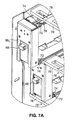
- FIG. 7 shows only two disk drives 36 1 and 36 2 , disk drive 36 2 being shown in a fully inserted position and disk drive 36 1 being shown in a partially inserted position.
- the disk backplane 54 is mounted to the rear of the rack 54, as shown.
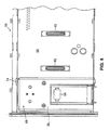
- the disk backplane 54 has eight electrical connectors 62 (FIG. 8) each in registration with a corresponding one of the slots 36.
- the connectors are thus arranged to enable the disk drives 36 1 to here 36 8 to be plugged into the electrical connectors 62, it being understood that while here eight disk drives 36 1 to 36 8 have been used for illustration, the system is here adapted for use with up to twenty four disk drives.
- the disk drives are electrically interconnected through conductors, not shown, in the disk backplane 54.
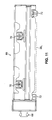
- FIGS. 9-11 an exemplary one of the housings 66 for disk drive 36 1 , the disk drive being shown in phantom in FIGS. 10 and 11, FIG. 9 showing the housing 66 without the disk drive.
- the disk drive chassis has a lock-handle 68 on the front panel thereof and screws 70 mounted on the opposing sides thereof for engagement with the sides of the disk drive, in a conventional manner.
- the disk drive housing 66 includes features according to the invention which reduce vibration occurring in the disk drive, from coupling to the rack 56 and thereby coupling through the rack 56 to the other disk drives in the rack 56. It has been found that when there are many disk drives in the rack 56, during operation of the disk drives, the vibration through the rack 56 can cause excessive vibration on the disk drives resulting in their malfunction.
- the housing 66 is formed with a plurality of, here four, legs 72, each of which has the resilient material 74 disposed around it, as shown.
- portions of the resilient material 74 project beyond the sides of the housing 66.
- the rack 56 (FIGS 7 and 7A). has a plurality of horizontal members 76. Upper and lower pairs of the horizontal members 76 have vertically opposing pairs of slots 78 therein.
- Each opposing pair of slots 78 is configured to engage the upper pair and lower pair of legs 72 with the resilient material 74 around such legs 72. This is more clearly illustrated in FIG. 7A.
- the resilient member presses firmly against the walls of the slots 78 to thereby cushion, and thus suppress, any vibrations produced during operation of the disk drive which may coupled to its housing 66 from coupling to the rack 56. That is, the vibrations coupled to the housing are dampened by the resilient, shock absorbing material 74 around the legs 72 and such vibrations are thereby de-coupled from the rack 56.
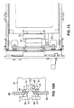
- a second technique used to decouple vibration produced during operation of the disk drive from the rack 56 is through the electrical interconnect arrangement used to connect the disk drive to the connector 62 (FIG. 8) on the disk backplane 54. More particularly, and referring also to FIG. 9, a flexible ribbon-type, or strap-type, electrical connector 57 (FIGS. 9,12, and 13) having a mounting member 59 (FIGS.12 and 12A) attached thereto to the rear of the ribbon-type connector 77 is used.
- the mounting member 59 has oval-shaped holes 61 (FIG. 12A) for receiving mounting screws 63.
- the rear of the housing 66 is provided with a mounting plate 65.
- the mounting plate 65 has a pair of screw receiving fixtures 67 attached thereto for receiving the mounting screws 63 after the holes 61 are aligned with fixtures 67.
- the screws 63 have a shoulder 69 which spaces the head of the screw 63 from the mounting member 59 when the screw is tightly threaded into the fixture 67.
- the shoulder 69 thus causes a gapG 1 between the mounting member and the head of the screw 63.
- the oval-shaped hole 61 allows for lateral back-and-forth movement of the screw 63 in the hole 61 even after the screw is threaded into the fixture 67, such back-and-forth movement being indicated by the arrows A in FIG. 12A.
- the arrangement is designed such that when the mounting member 59 is screwed to the mounting plate 65 with the screws 63, the mounting member 59 is prevented from being rigidly secured to the mounting plate 65. This is accomplished by constructing the screws 63 so that when fully inserted into their mating threaded holes, the shoulder 69 and oval-shaped holes 61 Referring to FIG. 13, the plug 71 of the flexible ribbon-type, or strap-type, electrical connector 57 is shown engaged with the plug 73 at the rear of the disk drive 36 1 . With such an arrangement as vibrations in the drive couple to the chassis and thus to the ribbon mounting member, such vibration will not could to the mounting plate because the two are not rigidly attached one to the other because of the mechanism described above.
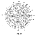
- the exemplary cable 52 0 is adapted to carry both fibre channel signals and non-fibre channel signals.
- the fibre channel signals include the data for storage in the disk drives and the non-fibre channel signals include the control signals described above for controlling the multiplexers in the port by-pass cards as well as other control signals for controlling the operation of the disk drives. It is noted that both the fibre channel signals and the non-fibre channel signals pass through the same cable. Thus, a single connector is used at each end of the cable for both the fibre channel signals and the non-fibre channel signals.
- the cable 52 0 is shown to have a central dielectric core 80.
- the core has around it the conventional quadrature-pair of electrically insulated conductors 82a-82d arranged for transmission of two pair of differential fibre channel signals.
- One pair of signals i.e., the signals of conductors 82a and 82b are the data from the I/O adapter to the port by-pass card, e.g., the data on 41 1 in FIG. 3
- the other pair of signals i.e., the signals of conductors 82c and 82d are the data from the port by-pass card to the I/O adapter, e.g., the data on 41 o in FIG. 3).
- an inner conductive shield 86 Disposed around the quadrature-pair of electrically insulated conductors 82a-82d is an inner conductive shield 86. Disposed around the inner conductive shield 86 are a plurality, here ten regularly spaced electrically insulated electrical conductors 88 which carry the non-fibre channel signals. e.g., for control signals. Disposed round the electrically insulated conductors 88 is an outer conductive shield 92. Disposed around the outer conductive shield 92 is a rubber-like sheath 94.
- the ends of the conductors 82a-82d and the ends of the ten conductors 86 are connected to lugs, or pins 85, at each of a pair of plugs 94a, 94b, as shown more clearly in FIG. 5B for plug 94a.
- the inner conductive shield 86 is connected to one of the lugs and the outer conductive shield 92 is connected to the conductive outer housing 93 of the plugs 94a, 94b. It is noted that each of the plugs is here a conventional 25-pin plug, thus here not all of the 25 pins are used.
- the fibre channel data passes through an inner, electro-statically shielded region of the transmission media provided by the cable and the control signals pass through an outer, electro-statically shielded region of the transmission media provided by the cable. Further is noted that only one plug is required at each end of the cable transmission of both the fiber channel signals and the non-fibre channel signals.
- FIG. 14 an alternative embodiment of the port by-pass card 34, here exemplary port A by-pass card 34 1 ', is shown in detail together with a B port by-pass card 34' 2 , and the disk drive section 14 1 coupled to the port A and port B by pass cards 34' 1 and 34' 2 , as indicated.
- Each one of the port by-pass cards 34' 1 and 34' 2 is identical in construction.
- a fail-over controller 100 is provided together with a fail-over switch 102.
- the fail-over controller 100 of the port A by-pass card 34' 1 is used to detect a signal from the director 20 0 via the I/O adapter 22 0 indicating that there is some "software" type error, as distinguished from a "hardware” type error, in the operation of the director 20 1 .
- a signal from the director 20 0 via the I/O adapter 22 0 indicating that there is some "software" type error, as distinguished from a "hardware” type error, in the operation of the director 20 1 .
- one type of "software" error in director 20 1 may cause director 20 1 to continue to request access to the disk drives in section 14 1 ; and such excessive "busy” is detected by director 20 0 .
- the director 20 0 issues a fail-over command to the fail-over controller 100 in the A port by-pass card 34 1 ,.
- the fail-over controller 100 of the A port by-pass card 34 produces a switching signal on line 104 for the fail-over switch 102 in the port B by-pass card 34 2 .
- the switch 102 in the port B by-pass card 34' 2 opens in response to the switching signal on line 104 thereby de-coupling the director 20 1 from the disk drives 36 1 through 36 8 in the disk drive section 14 1 .
- the switch 102 is in series with bus 41 1 described above in connection with FIG. 3.
- bus 41 1 is, when switch 102 is normally (i.e., during the normal, non-fail-over mode when switch 102 is closed) coupled to the A input of multiplexer 39 1 as described above in connection with FIG. 3.
- the switch 102 in the port B by-pass card 34' 2 opens in response to the switching signal on line 104 to de-couple the director 20 1 from the B ports of the disk drives 36 1 -36 8 in the disk drive section 14 1 .
- the fail-over controller 100 of the port B by-pass card 34' 2 is used to detect a signal from the director 20 1 via the I/O adapter 22 1 indicating that there is some "software" type error, as distinguished from a "hardware” type error, in the operation of the director 20 0 .
- the director 20 1 issues a fail-over command to the fail-over controller 100 in the port B by-pass card 34' 2 .
- the fail-over controller 100 of the port B by-pass card 34 2 produces a switching signal on line 106 for the fail-over switch 102 in the port A by-pass card 34 1 .
- the switch 102 in the port A by-pass card 34' 1 opens in response to the switching signal on line 106 thereby de-coupling the director 20 1 from the disk drives 36 1 through 36 8 in the disk drive section 14 1 .
- line 104 and 106 are disposed in the disk backplane 54 (FIG. 4).
- the fail-over controllers 100 provide port by-pass control via fail-over commands (e.g., reset and power control). This function is provided to effect a smooth and reliable transition in the case of as director fail-over when one director has to be taken out of the fibre channel "loop".
- the fail-over controllers 100 are able to process three commands:Card Reset, Card Power Off, and Card Power On. The sequence of these commands is as follows, considering exemplary the fail-over controller 100 of the port A by-pass card 34 1 : The command bus 108 to the fail-over controller 100 of the port A by-pass card 34' 1 from its associated (i.e., coupled) director 20 0 must start at Idle.
- a Command Verify command is issued by the associated director 20 0 .
- one of the action commands (Reset, Card Power On, Card Power Off) is issued, followed by an Execute_ ⁇ type>command where ⁇ type> is the desired action. If this sequence is followed, then when the Execute command is issued, the action will be performed by the remote port by-pass card, here the port B port by-pass card 34' 2 .
- the bus 108 then returns to Idle.
- the command bus 108 that carries these commands has three data bits plus a parity bit. Theses four bits form sixteen codes, as described below: C2 C1 C0 Parity Description 0 0 0 0 Parity Error (PE) 0 0 0 1 Idle 0 0 1 0 Card Reset 0 0 1 1 PE 0 1 0 0 Card Power Off 0 1 0 1 PE 0 1 1 0 PE 0 1 1 1 1 Execute Power On 9 0 0 0 0 Card Power Off 1 0 0 1 PE 1 0 1 0 PE 1 0 1 1 1 Execute Power Off 1 1 0 0 PE 1 1 0 1 Execute Reset 1 1 1 0 Command Verify 1 1 1 1 PE
- the control sequence is designed to detect hardware failures in the control bus 108 by forcing the bus state from idle (000) to Command Verify (111) to start the command sequence.
- the actual command of the combination code and the binary inverse e.g., Card Reset ⁇ 001> and Execute Reset ⁇ 110>
- This sequence control provides protection from code faults or execution errors that inadvertently write data to the fail-cover controller 100.
- the sequence state diagram is shown in FIG. 15.
- I/O adapters 22' 0 , 22 1 , and port by-pass sections 23' 1 , 23' 2 are shown for use in the redundant fibre channel networks 25 1 -25 4 (FIG. 1) here, in FIG. 16, being shown for exemplary redundant fibre channel network 25'.
- the I/O adapters 22' 0 and 22' 1 of network 25 1 each include a pair of fibre channel switching hubs 80A, 80B, as shown.
- Each one of the hubs 80A and 80B are identical in construction, an exemplary one thereof, here the hub 80A of I/O adapter 22' 0 being shown in detail.
- Such hub 80A is shown to include a fibre channel input 82 connected to the A port of the director 20 0 .
- the hub 80B of I/O adapter 22' 0 is coupled to the B port of director 20 0 .
- the hub 80A of I/O adapter 22 1 is coupled to the A port of director 20 1 and the hub 80B of I/O adapter 22' 1 is coupled to the B port of director 20 1 .
- the number of disk drives in each disk drive section 14' 1 and 14' 2 have doubled from eight to here sixteen (i.e., disk drives 36 1 to 36 16 .
- such hub is shown to include drivers 84, 86. 88, 90, 92, and 94 and multiplexers 96 and 98, all arranged as shown.
- the one of the pair of input ports of the multiplexers 96, 98 is coupled to its output is selected by the control signal fed to lines 100 and 102, respectively, as indicated.
- the control signal on line 100 is fed to multiplexer 96 and the control signal on line 102 is fed to multiplexer 102.
- control signals on lines 100 and 102 are produced by the director 20 1 for the hubs 80A and 80B in I/O adapter 22' 0 and the equivalent control signals for the hubs 80A and 80B of I/O adapters 22' 1 are produced by the director 20 1 .
- each one is identical in construction, an exemplary one thereof, here section 23' 1 being shown in detail to include a port A by-pass card 34' 1 and a port B by-pass card 34' 2 .
- each port by-pass card 34' 1 and 34' 2 includes two redundant ones of the port by-pass cards described above in connection with FIG. 3.
- the upper port A by-pass card 34 1 services eight disk drives in disk drive section 14 1
- the lower port A by-pass card 34 1 services another set of here eight disk drives in disk drive section 14' 1 .
- the hub 80A enables many different coupling configurations with the disk drive sections 14 1 and 14' 1 depending on the logic state of the signals provided by the director 20 0 to control lines 100 and 102 of the multiplexers 96, 98.
- the data from the A port of director 20 0 is passed through driver 84, then through driver 88 then to the upper port A by-pass card 34 1 , then to driver 90 then through multiplexer 100 and back to the A port of the director 20 0 through driver 86, thus by-passing the lower port A by-pass card 34 1 .
- the data from the A port of director 20 0 is passed through driver 84, then through multiplexer 102, then through driver 94, then through the lower port A by-pass card 34 1 , then to driver 92 then through multiplexer 100 and back to the A port of the director 20 0 through driver 86, thus by-passing the upper port A by-pass card 34 1 .
- the data from the A port of director 20 0 is passed through driver 84, then driver 88 then through the upper port A by-pass card 34 1 , then through driver 90, then through multiplexer 102, then through driver 94, then to the lower A port by-pass card 34 1 , then through driver 92, then through multiplexer 100, then back to the A port of director 20 0 through driver 86.
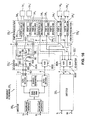
- I/O adapter 22 4 having a pair of ports P 1 , P 2 adapted for coupling to director 20 4 and a plurality of, here four, ports P 3 -P 6 adapted for communication with the host computer, here four host computer sections 12 1 -12 4 of the host computer 12 (FIG. 1) through a fibre channel hub 201.
- the hub 201 of I/O adapter 22 4 includes a plurality of electro-optical transceivers 200 1 - 200 4 , each one including a laser for transmitting data to the host computer section coupled thereto and a laser receiver for receiving data from such coupled host computer section.
- transceivers 200 1 - 200 4 are coupled to host computer sections 12 1 - 12 4 , respectively, as indicated.
- Each one of the transceivers 200 1 - 200 4 is coupled to a corresponding one of a plurality of, here four, switching sections 202 1 - 202 4 , respectively as indicated.
- Each one of the switching sections includes a receiver re-timer 204, a transmit re-timer 206 and a multiplexer 208, arranged as shown.
- Each one of the multiplexers 208 in sections 202 1 -202 4 is controlled by control signals on lines L1-L4, respectively as indicated.
- the control signals on lines L1-L4 are supplied by a multiplexer controller 210.
- the control signals supplied by the multiplexer controller 210 are produced in accordance with a control signal supplied by the director 204 coupled to the I/O adapter 22 4 .
- the arrangement controls the distribution between director 20 4 and a selected one, or ones of the host computer sections 200 1 -200 4 . More particularly, and considering data from the director 20 4 to the data from the director 20 4 , such data passes to an input of multiplexer section 202 4 . The data is able to pass to the transceiver 200 4 or pass to multiplexer section 202 3 selectively in accordance with the control signal on line L4. Thus, if it is desired to communicate with host computer section 12 4 , the control signal on line L1 selects port A of multiplexer 208 in section 202 4 .
- control signal on line L4 causes the data at the B port of the multiplexer 208 of such multiplexer section 202 4 to pass directly to the output of such section 202 4 .
- port A when port A is selected to enable communication with the host computer section 12 4 , the data passes to the host computer section 12 4 via the transmit re-timer 206 and data from the host computer section 12 4 via the receive re-timer 204.
- each one of the front-end directors has a pair of ports and therefore the I/O adapter connected to such director has a pair hubs 201 each one being coupled to a corresponding one of the ports of the front-end director.
- FIG. 18 a method for testing the signal integrity of the signals on the system backplane 50 (FIG. 4) will be described.
- the directors 20 0 - 20 15 and I/O adapters 22 0 -22 15 are plugged into an array of slots on opposite sides in the system backplane 50.
- the arrangement is described in more detail in the above-referenced copending patent application Serial NO. 09/224,194 filed December 30, 1998, entitled DATA STORAGE SYSTEM, inventor Mark Zani.
- the system backplane 50n has a plurality of slots 32 0 - 32 19 , the slots in the front surface thereof being adapted to receive the front-end and the rear-end directors and the memories and the slots in the back surface thereof being adapted to receive the front-end and the rear-end I/O adapters.
- Each slot has a large plurality of pins for receiving the directors, I/O adapters and memories, as shown in FIGS. 18A and 19B.
- the buses TH, TL, BH, and BL appear to the highspeed data thereon as transmission lines.
- the system backplane 50 has typically several hundred pins for each director slot.
- the following test procedure is used to test the signal integrity at each one of the slots. It should be understood that because of different loading effects at various slots along the busses, the waveform of the signals on a bus would appear slightly different from slot to slot.
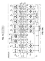
- a test board, or card 300 is provided, such test board 300 being shown in FIG 18.
- the test board 300 is adapted to replace, during a test mode, each one of the directors and memories and thereby enable the signal waveforms at the pins in the slot occupied by such one of the directors and memories to be examined.
- the test board 300 is shown to include a plurality of transceivers 302 coupled to each one of the pins of the board 300.
- the transceivers 302 are coupled to a multiplexer section 304.
- the multiplexer section has seven multiplexers 303 1 - 307 7 , it being understood that for several hundred pins there would be a significantly larger number of multiplexers.
- the board 300 has a multiplexer control section 306 which produces control signal on line N 1 -N 7 for each one of the multiplexers in the multiplexer section 304. In response to the control signals a selected one of the pins is thereby coupled to an output port P o of the test card 300.
- the signal at each one of the pins can be selectively coupled to the output port P o .
- the output port P o is coupled to a scope 310.
- a personal computer PC 312 is used to control the multiplexer control section 306 and scope 310.
- the signal at each one of the pins is sequentially examined with the scope 310 and recorded in the PC 312.
- the test board 300 is placed in one of the slots 32 0 -32 15 .
- the test board is plugged into a different one of the slots and the process is repeated for the newly positioned test board. The process is repeated until the signal waveform at each one of the pins in at slot and at each one of the slots is individually analyzed with the backplane 50 under fully loaded conditions (i.e., with the directors and memories, other than the director or memory normally in the slot being tested) and the I/ O adapters plugged into the system backplane.
Landscapes
- Debugging And Monitoring (AREA)
- Communication Cables (AREA)
Abstract
Description
Another fibre channel arrangement is described in U. S. Patent 5,729,763 entitled "Data Storage System", inventor Eli Leshem, issued March 17, 1998, assigned to the same assignee as the present invention.
| C2 | C1 | | Parity | Description | |
| 0 | 0 | 0 | 0 | Parity Error (PE) | |
| 0 | 0 | 0 | 1 | Idle | |
| 0 | 0 | 1 | 0 | | |
| 0 | 0 | 1 | 1 | | |
| 0 | 1 | 0 | 0 | | |
| 0 | 1 | 0 | 1 | | |
| 0 | 1 | 1 | 0 | | |
| 0 | 1 | 1 | 1 | Execute Power On | |
| 9 | 0 | 0 | 0 | | |
| 1 | 0 | 0 | 1 | | |
| 1 | 0 | 1 | 0 | | |
| 1 | 0 | 1 | 1 | Execute | |
| 1 | 1 | 0 | 0 | | |
| 1 | 1 | 0 | 1 | Execute | |
| 1 | 1 | 1 | 0 | Command Verify | |
| 1 | 1 | 1 | 1 | PE |
Claims (5)
- A method for transmitting fibre channel signals and non-fibre channel signals, comprising:providing a cable having a connector at each end thereof;transmitting both the fibre-channel signals and the non-fibre channel signals through the cable between the connectors.
- The method recited in claim 1 wherein the non- fibre channel signals are transmitted in outer region of the cable and the fibre channel signals are transmitted in a region of the cable interior to the outer region.
- A cable, comprising:a pair of connectors each one having a plurality of pins;a first plurality of conductors arrange to transmit fibre channel signals, ends of such conductors being connected to pins in each one of the pair of connectors;a second plurality of conductors disposed around the first plurality of conductors, ends of such conductors being connected to pins in each one of the pair of connectors.
- The cable recited in claim 3 including a conductive shield disposed between the first plurality of conductors and the second plurality of conductors.
- The cable recited in claim 4 including a second conductive shield disposed about both the first and second pluralities of conductors.
Applications Claiming Priority (2)
| Application Number | Priority Date | Filing Date | Title |
|---|---|---|---|
| US09/474,886 US6466718B1 (en) | 1999-12-29 | 1999-12-29 | Method and apparatus for transmitting fiber-channel and non-fiber channel signals through common cable |
| US474886 | 1999-12-29 |
Publications (3)
| Publication Number | Publication Date |
|---|---|
| EP1113462A2 true EP1113462A2 (en) | 2001-07-04 |
| EP1113462A3 EP1113462A3 (en) | 2003-05-14 |
| EP1113462B1 EP1113462B1 (en) | 2006-10-25 |
Family
ID=23885349
Family Applications (1)
| Application Number | Title | Priority Date | Filing Date |
|---|---|---|---|
| EP00311748A Expired - Lifetime EP1113462B1 (en) | 1999-12-29 | 2000-12-28 | Method for transmitting fibre-channel and non-fibre channel signals through common cable. |
Country Status (3)
| Country | Link |
|---|---|
| US (2) | US6466718B1 (en) |
| EP (1) | EP1113462B1 (en) |
| DE (1) | DE60031499T2 (en) |
Families Citing this family (70)
| Publication number | Priority date | Publication date | Assignee | Title |
|---|---|---|---|---|
| US6466718B1 (en) * | 1999-12-29 | 2002-10-15 | Emc Corporation | Method and apparatus for transmitting fiber-channel and non-fiber channel signals through common cable |
| JP2002330506A (en) * | 2000-03-17 | 2002-11-15 | Seiko Epson Corp | Distribution board, junction box, outlet box, plug with electric cord, terminal box for outlet box, table tap and home network system |
| GB2364831A (en) * | 2000-07-12 | 2002-02-06 | Mitel Semiconductor Ab | Optical fibre cable to extend electrical bus |
| US20040225804A1 (en) * | 2000-12-05 | 2004-11-11 | Intel Corporation | Power supply with bus hub |
| US7392445B2 (en) * | 2003-09-11 | 2008-06-24 | International Business Machines Corporation | Autonomic bus reconfiguration for fault conditions |
| US20060093282A1 (en) * | 2004-10-29 | 2006-05-04 | Christian Shepherd | Method and apparatus for providing connector keying and identification for unidirectional fiber cables |
| US7311526B2 (en) | 2005-09-26 | 2007-12-25 | Apple Inc. | Magnetic connector for electronic device |
| US7351066B2 (en) | 2005-09-26 | 2008-04-01 | Apple Computer, Inc. | Electromagnetic connector for electronic device |
| EP1772795A1 (en) * | 2005-10-10 | 2007-04-11 | STMicroelectronics (Research & Development) Limited | Fast buffer pointer across clock |
| US8472767B2 (en) | 2006-05-19 | 2013-06-25 | Corning Cable Systems Llc | Fiber optic cable and fiber optic cable assembly for wireless access |
| US20070292136A1 (en) * | 2006-06-16 | 2007-12-20 | Michael Sauer | Transponder for a radio-over-fiber optical fiber cable |
| US8442353B2 (en) * | 2006-08-03 | 2013-05-14 | The Regents Of The University Of California | Incorporation of mathematical constraints in methods for dose reduction and image enhancement in tomography |
| US7627250B2 (en) | 2006-08-16 | 2009-12-01 | Corning Cable Systems Llc | Radio-over-fiber transponder with a dual-band patch antenna system |
| US7787823B2 (en) | 2006-09-15 | 2010-08-31 | Corning Cable Systems Llc | Radio-over-fiber (RoF) optical fiber cable system with transponder diversity and RoF wireless picocellular system using same |
| US7848654B2 (en) | 2006-09-28 | 2010-12-07 | Corning Cable Systems Llc | Radio-over-fiber (RoF) wireless picocellular system with combined picocells |
| US8873585B2 (en) | 2006-12-19 | 2014-10-28 | Corning Optical Communications Wireless Ltd | Distributed antenna system for MIMO technologies |
| US8111998B2 (en) | 2007-02-06 | 2012-02-07 | Corning Cable Systems Llc | Transponder systems and methods for radio-over-fiber (RoF) wireless picocellular systems |
| US20100054746A1 (en) | 2007-07-24 | 2010-03-04 | Eric Raymond Logan | Multi-port accumulator for radio-over-fiber (RoF) wireless picocellular systems |
| US8175459B2 (en) | 2007-10-12 | 2012-05-08 | Corning Cable Systems Llc | Hybrid wireless/wired RoF transponder and hybrid RoF communication system using same |
| WO2009081376A2 (en) | 2007-12-20 | 2009-07-02 | Mobileaccess Networks Ltd. | Extending outdoor location based services and applications into enclosed areas |
| US7841776B2 (en) | 2008-09-30 | 2010-11-30 | Apple Inc. | Magnetic connector with optical signal path |
| US9791634B2 (en) | 2008-09-30 | 2017-10-17 | Apple Inc. | Magnetic connector with optical signal path |
| WO2010091004A1 (en) | 2009-02-03 | 2010-08-12 | Corning Cable Systems Llc | Optical fiber-based distributed antenna systems, components, and related methods for calibration thereof |
| US9673904B2 (en) | 2009-02-03 | 2017-06-06 | Corning Optical Communications LLC | Optical fiber-based distributed antenna systems, components, and related methods for calibration thereof |
| AU2010210766A1 (en) | 2009-02-03 | 2011-09-15 | Corning Cable Systems Llc | Optical fiber-based distributed antenna systems, components, and related methods for monitoring and configuring thereof |
| US8548330B2 (en) | 2009-07-31 | 2013-10-01 | Corning Cable Systems Llc | Sectorization in distributed antenna systems, and related components and methods |
| US8535088B2 (en) | 2009-10-20 | 2013-09-17 | Apple Inc. | Magnetic connector having a unitary housing |
| US8280259B2 (en) | 2009-11-13 | 2012-10-02 | Corning Cable Systems Llc | Radio-over-fiber (RoF) system for protocol-independent wired and/or wireless communication |
| US8275265B2 (en) | 2010-02-15 | 2012-09-25 | Corning Cable Systems Llc | Dynamic cell bonding (DCB) for radio-over-fiber (RoF)-based networks and communication systems and related methods |
| US20110268446A1 (en) | 2010-05-02 | 2011-11-03 | Cune William P | Providing digital data services in optical fiber-based distributed radio frequency (rf) communications systems, and related components and methods |
| US9525488B2 (en) | 2010-05-02 | 2016-12-20 | Corning Optical Communications LLC | Digital data services and/or power distribution in optical fiber-based distributed communications systems providing digital data and radio frequency (RF) communications services, and related components and methods |
| EP2606707A1 (en) | 2010-08-16 | 2013-06-26 | Corning Cable Systems LLC | Remote antenna clusters and related systems, components, and methods supporting digital data signal propagation between remote antenna units |
| US9252874B2 (en) | 2010-10-13 | 2016-02-02 | Ccs Technology, Inc | Power management for remote antenna units in distributed antenna systems |
| CN203504582U (en) | 2011-02-21 | 2014-03-26 | 康宁光缆系统有限责任公司 | Distributed antenna system and power supply device for distributing power therein |
| CN103609146B (en) | 2011-04-29 | 2017-05-31 | 康宁光缆系统有限责任公司 | Systems, methods and apparatus for increasing radio frequency (RF) power in a distributed antenna system |
| WO2012148938A1 (en) | 2011-04-29 | 2012-11-01 | Corning Cable Systems Llc | Determining propagation delay of communications in distributed antenna systems, and related components, systems and methods |
| US8888500B2 (en) | 2011-06-30 | 2014-11-18 | Apple Inc. | Robust magnetic connector |
| US9065205B2 (en) | 2011-08-11 | 2015-06-23 | Apple Inc. | Connector insert having a cable crimp portion with protrusions and a receptacle having label in the front |
| EP2832012A1 (en) | 2012-03-30 | 2015-02-04 | Corning Optical Communications LLC | Reducing location-dependent interference in distributed antenna systems operating in multiple-input, multiple-output (mimo) configuration, and related components, systems, and methods |
| WO2013162988A1 (en) | 2012-04-25 | 2013-10-31 | Corning Cable Systems Llc | Distributed antenna system architectures |
| EP2883416A1 (en) | 2012-08-07 | 2015-06-17 | Corning Optical Communications Wireless Ltd. | Distribution of time-division multiplexed (tdm) management services in a distributed antenna system, and related components, systems, and methods |
| US9455784B2 (en) | 2012-10-31 | 2016-09-27 | Corning Optical Communications Wireless Ltd | Deployable wireless infrastructures and methods of deploying wireless infrastructures |
| EP2926466A1 (en) | 2012-11-29 | 2015-10-07 | Corning Optical Communications LLC | HYBRID INTRA-CELL / INTER-CELL REMOTE UNIT ANTENNA BONDING IN MULTIPLE-INPUT, MULTIPLE-OUTPUT (MIMO) DISTRIBUTED ANTENNA SYSTEMS (DASs) |
| US9647758B2 (en) | 2012-11-30 | 2017-05-09 | Corning Optical Communications Wireless Ltd | Cabling connectivity monitoring and verification |
| WO2014199380A1 (en) | 2013-06-12 | 2014-12-18 | Corning Optical Communications Wireless, Ltd. | Time-division duplexing (tdd) in distributed communications systems, including distributed antenna systems (dass) |
| CN105452951B (en) | 2013-06-12 | 2018-10-19 | 康宁光电通信无线公司 | Voltage type optical directional coupler |
| US9247543B2 (en) | 2013-07-23 | 2016-01-26 | Corning Optical Communications Wireless Ltd | Monitoring non-supported wireless spectrum within coverage areas of distributed antenna systems (DASs) |
| US9661781B2 (en) | 2013-07-31 | 2017-05-23 | Corning Optical Communications Wireless Ltd | Remote units for distributed communication systems and related installation methods and apparatuses |
| US9385810B2 (en) | 2013-09-30 | 2016-07-05 | Corning Optical Communications Wireless Ltd | Connection mapping in distributed communication systems |
| US9178635B2 (en) | 2014-01-03 | 2015-11-03 | Corning Optical Communications Wireless Ltd | Separation of communication signal sub-bands in distributed antenna systems (DASs) to reduce interference |
| US9775123B2 (en) | 2014-03-28 | 2017-09-26 | Corning Optical Communications Wireless Ltd. | Individualized gain control of uplink paths in remote units in a distributed antenna system (DAS) based on individual remote unit contribution to combined uplink power |
| US9357551B2 (en) | 2014-05-30 | 2016-05-31 | Corning Optical Communications Wireless Ltd | Systems and methods for simultaneous sampling of serial digital data streams from multiple analog-to-digital converters (ADCS), including in distributed antenna systems |
| US9525472B2 (en) | 2014-07-30 | 2016-12-20 | Corning Incorporated | Reducing location-dependent destructive interference in distributed antenna systems (DASS) operating in multiple-input, multiple-output (MIMO) configuration, and related components, systems, and methods |
| US9730228B2 (en) | 2014-08-29 | 2017-08-08 | Corning Optical Communications Wireless Ltd | Individualized gain control of remote uplink band paths in a remote unit in a distributed antenna system (DAS), based on combined uplink power level in the remote unit |
| US9602210B2 (en) | 2014-09-24 | 2017-03-21 | Corning Optical Communications Wireless Ltd | Flexible head-end chassis supporting automatic identification and interconnection of radio interface modules and optical interface modules in an optical fiber-based distributed antenna system (DAS) |
| US9420542B2 (en) | 2014-09-25 | 2016-08-16 | Corning Optical Communications Wireless Ltd | System-wide uplink band gain control in a distributed antenna system (DAS), based on per band gain control of remote uplink paths in remote units |
| US10659163B2 (en) | 2014-09-25 | 2020-05-19 | Corning Optical Communications LLC | Supporting analog remote antenna units (RAUs) in digital distributed antenna systems (DASs) using analog RAU digital adaptors |
| WO2016071902A1 (en) | 2014-11-03 | 2016-05-12 | Corning Optical Communications Wireless Ltd. | Multi-band monopole planar antennas configured to facilitate improved radio frequency (rf) isolation in multiple-input multiple-output (mimo) antenna arrangement |
| WO2016075696A1 (en) | 2014-11-13 | 2016-05-19 | Corning Optical Communications Wireless Ltd. | Analog distributed antenna systems (dass) supporting distribution of digital communications signals interfaced from a digital signal source and analog radio frequency (rf) communications signals |
| US9729267B2 (en) | 2014-12-11 | 2017-08-08 | Corning Optical Communications Wireless Ltd | Multiplexing two separate optical links with the same wavelength using asymmetric combining and splitting |
| WO2016098109A1 (en) | 2014-12-18 | 2016-06-23 | Corning Optical Communications Wireless Ltd. | Digital interface modules (dims) for flexibly distributing digital and/or analog communications signals in wide-area analog distributed antenna systems (dass) |
| WO2016098111A1 (en) | 2014-12-18 | 2016-06-23 | Corning Optical Communications Wireless Ltd. | Digital- analog interface modules (da!ms) for flexibly.distributing digital and/or analog communications signals in wide-area analog distributed antenna systems (dass) |
| US20160249365A1 (en) | 2015-02-19 | 2016-08-25 | Corning Optical Communications Wireless Ltd. | Offsetting unwanted downlink interference signals in an uplink path in a distributed antenna system (das) |
| US9681313B2 (en) | 2015-04-15 | 2017-06-13 | Corning Optical Communications Wireless Ltd | Optimizing remote antenna unit performance using an alternative data channel |
| US9948349B2 (en) | 2015-07-17 | 2018-04-17 | Corning Optical Communications Wireless Ltd | IOT automation and data collection system |
| US10560214B2 (en) | 2015-09-28 | 2020-02-11 | Corning Optical Communications LLC | Downlink and uplink communication path switching in a time-division duplex (TDD) distributed antenna system (DAS) |
| US10236924B2 (en) | 2016-03-31 | 2019-03-19 | Corning Optical Communications Wireless Ltd | Reducing out-of-channel noise in a wireless distribution system (WDS) |
| US10821290B2 (en) * | 2018-07-13 | 2020-11-03 | Greatbatch Ltd. | Lead adaptor double port for implantable neuro-stimulation system |
| US11424573B2 (en) | 2020-09-24 | 2022-08-23 | Apple Inc. | Magnetic connectors with self-centering floating contacts |
| US12138466B2 (en) | 2021-03-12 | 2024-11-12 | Greatbatch Ltd. | Cable-less lead adapter for implantable neurostimulator system |
Family Cites Families (20)
| Publication number | Priority date | Publication date | Assignee | Title |
|---|---|---|---|---|
| US4597631A (en) * | 1982-12-02 | 1986-07-01 | The United States Of America As Represented By The Secretary Of The Navy | Printed circuit card hybrid |
| US4678264A (en) * | 1983-03-30 | 1987-07-07 | Amp Incorporated | Electrical and fiber optic connector assembly |
| US4767181A (en) * | 1983-11-17 | 1988-08-30 | American Telephone And Telegraph Company | Electrical/lightwave connection arrangement |
| US4964814A (en) * | 1986-10-03 | 1990-10-23 | Minnesota Mining And Manufacturing Co. | Shielded and grounded connector system for coaxial cables |
| US4896939A (en) * | 1987-10-30 | 1990-01-30 | D. G. O'brien, Inc. | Hybrid fiber optic/electrical cable and connector |
| US4895426A (en) * | 1988-09-20 | 1990-01-23 | The Boeing Company | Electrically conducting reinforced optical fiber |
| JPH02129610A (en) * | 1988-11-09 | 1990-05-17 | Takashi Mori | Optical connectors and optical terminals |
| US5206939A (en) | 1990-09-24 | 1993-04-27 | Emc Corporation | System and method for disk mapping and data retrieval |
| US5140659A (en) * | 1991-01-28 | 1992-08-18 | Hughes Aircraft Company | Combination optical fiber and electrical connector |
| US5125854A (en) * | 1991-07-16 | 1992-06-30 | Molex Incorporated | Modular electrical connector |
| GB9420935D0 (en) * | 1994-10-17 | 1994-11-30 | Amp Gmbh | Multi-position coaxial cable connector |
| AU4197796A (en) * | 1994-11-14 | 1996-06-06 | New Media Corp. | Shielded audio/digital communication cable system |
| EP0713111A1 (en) * | 1994-11-15 | 1996-05-22 | The Whitaker Corporation | Sealed multiposition fiber optic connector |
| US5767999A (en) * | 1996-05-02 | 1998-06-16 | Vixel Corporation | Hot-pluggable/interchangeable circuit module and universal guide system having a standard form factor |
| US5744756A (en) * | 1996-07-29 | 1998-04-28 | Minnesota Mining And Manufacturing Company | Blown microfiber insulated cable |
| US5917977A (en) * | 1997-09-16 | 1999-06-29 | Siecor Corporation | Composite cable |
| US6035085A (en) * | 1997-09-23 | 2000-03-07 | Sony Corporation | Digital and analog compatible triaxial cable system |
| US6206728B1 (en) * | 1999-02-22 | 2001-03-27 | Molex Incorporated | Shielded electrical connector system |
| US6524702B1 (en) * | 1999-08-12 | 2003-02-25 | Dow Global Technologies Inc. | Electrical devices having polymeric members |
| US6466718B1 (en) * | 1999-12-29 | 2002-10-15 | Emc Corporation | Method and apparatus for transmitting fiber-channel and non-fiber channel signals through common cable |
-
1999
- 1999-12-29 US US09/474,886 patent/US6466718B1/en not_active Expired - Lifetime
-
2000
- 2000-12-28 EP EP00311748A patent/EP1113462B1/en not_active Expired - Lifetime
- 2000-12-28 DE DE60031499T patent/DE60031499T2/en not_active Expired - Lifetime
-
2002
- 2002-05-23 US US10/154,269 patent/US6826337B2/en not_active Expired - Lifetime
Also Published As
| Publication number | Publication date |
|---|---|
| US6826337B2 (en) | 2004-11-30 |
| US20030012528A1 (en) | 2003-01-16 |
| US6466718B1 (en) | 2002-10-15 |
| DE60031499D1 (en) | 2006-12-07 |
| EP1113462B1 (en) | 2006-10-25 |
| EP1113462A3 (en) | 2003-05-14 |
| DE60031499T2 (en) | 2007-08-30 |
Similar Documents
| Publication | Publication Date | Title |
|---|---|---|
| EP1113462B1 (en) | Method for transmitting fibre-channel and non-fibre channel signals through common cable. | |
| EP1113363B1 (en) | Fibre channel data storage system fail-over mechanism | |
| US6574687B1 (en) | Fibre channel data storage system | |
| US5870630A (en) | System for online SCSI drive repair utilizing detachable secondary I/O buses pigtailed to primary I/O bus wherein each secondary I/O bus has a length in excess of 100mm | |
| US6889345B2 (en) | System and method for locating a failed storage device in a data storage system | |
| US5694615A (en) | Storage system having storage units interconnected to form multiple loops to provide simultaneous access from multiple hosts | |
| US5495584A (en) | SCSI bus concatenator/splitter | |
| DE602004010303T2 (en) | MULTIPLE INTERFACES IN A MEMORY CASE | |
| US6799224B1 (en) | High speed fault tolerant mass storage network information server | |
| EP2517110B1 (en) | Configurable interconnection system | |
| US5455911A (en) | Communications protocol for use in transferring data over a serial bus | |
| US6615315B1 (en) | Fibre channel data storage system having improved fro-end I/O adapted hub | |
| EP0752658B1 (en) | Method and apparatus for passive loopback testing of software-controllable parallel ports | |
| US6351786B2 (en) | VXI backplane system improvements and methods | |
| US6378084B1 (en) | Enclosure processor with failover capability | |
| KR100883005B1 (en) | High Availability Mass Storage Systems and How to Create Them | |
| US6636934B1 (en) | Fiber channel port by-pass selector section for dual ported disk drives | |
| US6560683B1 (en) | Fibre channel data storage system having improved rear-end I/O adapted hub | |
| US6496951B1 (en) | Method for testing signal integrity in a data storage system | |
| US5577096A (en) | Transmission system having stand-by line switching facility | |
| US6430686B1 (en) | Disk subsystem with multiple configurable interfaces | |
| US5881249A (en) | I/O bus | |
| US6567890B1 (en) | Fibre channel port by-pass selector section for dual ported disk drives | |
| US7111066B2 (en) | Method of operating a storage device | |
| CN100419701C (en) | Method and apparatus for autonomous bus reconfiguration for fault conditions |
Legal Events
| Date | Code | Title | Description |
|---|---|---|---|
| PUAI | Public reference made under article 153(3) epc to a published international application that has entered the european phase |
Free format text: ORIGINAL CODE: 0009012 |
|
| AK | Designated contracting states |
Kind code of ref document: A2 Designated state(s): AT BE CH CY DE DK ES FI FR GB GR IE IT LI LU MC NL PT SE TR |
|
| AX | Request for extension of the european patent |
Free format text: AL;LT;LV;MK;RO;SI |
|
| PUAL | Search report despatched |
Free format text: ORIGINAL CODE: 0009013 |
|
| AK | Designated contracting states |
Designated state(s): AT BE CH CY DE DK ES FI FR GB GR IE IT LI LU MC NL PT SE TR |
|
| AX | Request for extension of the european patent |
Extension state: AL LT LV MK RO SI |
|
| RIC1 | Information provided on ipc code assigned before grant |
Ipc: 7H 01R 23/66 B Ipc: 7H 01B 11/22 A Ipc: 7H 01B 11/06 B |
|
| 17P | Request for examination filed |
Effective date: 20030806 |
|
| AKX | Designation fees paid |
Designated state(s): DE GB |
|
| 17Q | First examination report despatched |
Effective date: 20040910 |
|
| GRAP | Despatch of communication of intention to grant a patent |
Free format text: ORIGINAL CODE: EPIDOSNIGR1 |
|
| RTI1 | Title (correction) |
Free format text: METHOD FOR TRANSMITTING FIBRE-CHANNEL AND NON-FIBRE CHANNEL SIGNALS THROUGH COMMON CABLE. |
|
| GRAS | Grant fee paid |
Free format text: ORIGINAL CODE: EPIDOSNIGR3 |
|
| GRAA | (expected) grant |
Free format text: ORIGINAL CODE: 0009210 |
|
| AK | Designated contracting states |
Kind code of ref document: B1 Designated state(s): DE GB |
|
| REG | Reference to a national code |
Ref country code: GB Ref legal event code: FG4D |
|
| RIC1 | Information provided on ipc code assigned before grant |
Ipc: H01B 11/06 20060101ALI20060915BHEP Ipc: H01R 12/24 20060101ALI20060915BHEP Ipc: H01B 11/22 20060101AFI20060915BHEP |
|
| REF | Corresponds to: |
Ref document number: 60031499 Country of ref document: DE Date of ref document: 20061207 Kind code of ref document: P |
|
| PLBE | No opposition filed within time limit |
Free format text: ORIGINAL CODE: 0009261 |
|
| STAA | Information on the status of an ep patent application or granted ep patent |
Free format text: STATUS: NO OPPOSITION FILED WITHIN TIME LIMIT |
|
| 26N | No opposition filed |
Effective date: 20070726 |
|
| PGFP | Annual fee paid to national office [announced via postgrant information from national office to epo] |
Ref country code: GB Payment date: 20071227 Year of fee payment: 8 |
|
| GBPC | Gb: european patent ceased through non-payment of renewal fee |
Effective date: 20081228 |
|
| PG25 | Lapsed in a contracting state [announced via postgrant information from national office to epo] |
Ref country code: GB Free format text: LAPSE BECAUSE OF NON-PAYMENT OF DUE FEES Effective date: 20081228 |
|
| PGFP | Annual fee paid to national office [announced via postgrant information from national office to epo] |
Ref country code: DE Payment date: 20191119 Year of fee payment: 20 |
|
| REG | Reference to a national code |
Ref country code: DE Ref legal event code: R071 Ref document number: 60031499 Country of ref document: DE |