EP1113428A2 - Package structure for a hybrid optical module and method of producing the same - Google Patents
Package structure for a hybrid optical module and method of producing the same Download PDFInfo
- Publication number
- EP1113428A2 EP1113428A2 EP00311193A EP00311193A EP1113428A2 EP 1113428 A2 EP1113428 A2 EP 1113428A2 EP 00311193 A EP00311193 A EP 00311193A EP 00311193 A EP00311193 A EP 00311193A EP 1113428 A2 EP1113428 A2 EP 1113428A2
- Authority
- EP
- European Patent Office
- Prior art keywords
- resin package
- package
- optical module
- metal frame
- components
- Prior art date
- Legal status (The legal status is an assumption and is not a legal conclusion. Google has not performed a legal analysis and makes no representation as to the accuracy of the status listed.)
- Withdrawn
Links
- 230000003287 optical effect Effects 0.000 title claims abstract description 67
- 238000000034 method Methods 0.000 title claims description 23
- 239000011347 resin Substances 0.000 claims abstract description 61
- 229920005989 resin Polymers 0.000 claims abstract description 61
- 229910052751 metal Inorganic materials 0.000 claims abstract description 48
- 239000002184 metal Substances 0.000 claims abstract description 48
- 238000007493 shaping process Methods 0.000 claims description 4
- 238000005452 bending Methods 0.000 claims description 2
- 230000000191 radiation effect Effects 0.000 abstract description 5
- 229910052782 aluminium Inorganic materials 0.000 abstract description 2
- XAGFODPZIPBFFR-UHFFFAOYSA-N aluminium Chemical compound [Al] XAGFODPZIPBFFR-UHFFFAOYSA-N 0.000 abstract description 2
- 230000002411 adverse Effects 0.000 description 5
- 238000010438 heat treatment Methods 0.000 description 5
- 230000002708 enhancing effect Effects 0.000 description 2
- 230000005855 radiation Effects 0.000 description 2
- RYGMFSIKBFXOCR-UHFFFAOYSA-N Copper Chemical compound [Cu] RYGMFSIKBFXOCR-UHFFFAOYSA-N 0.000 description 1
- 230000004075 alteration Effects 0.000 description 1
- 239000000919 ceramic Substances 0.000 description 1
- 229910052802 copper Inorganic materials 0.000 description 1
- 239000010949 copper Substances 0.000 description 1
- 239000000463 material Substances 0.000 description 1
- 238000002844 melting Methods 0.000 description 1
- 230000008018 melting Effects 0.000 description 1
- 238000012544 monitoring process Methods 0.000 description 1
- 238000004080 punching Methods 0.000 description 1
- 239000000758 substrate Substances 0.000 description 1
Images

Classifications
-
- G—PHYSICS
- G11—INFORMATION STORAGE
- G11B—INFORMATION STORAGE BASED ON RELATIVE MOVEMENT BETWEEN RECORD CARRIER AND TRANSDUCER
- G11B7/00—Recording or reproducing by optical means, e.g. recording using a thermal beam of optical radiation by modifying optical properties or the physical structure, reproducing using an optical beam at lower power by sensing optical properties; Record carriers therefor
- G11B7/12—Heads, e.g. forming of the optical beam spot or modulation of the optical beam
- G11B7/22—Apparatus or processes for the manufacture of optical heads, e.g. assembly
-
- H—ELECTRICITY
- H01—ELECTRIC ELEMENTS
- H01L—SEMICONDUCTOR DEVICES NOT COVERED BY CLASS H10
- H01L25/00—Assemblies consisting of a plurality of individual semiconductor or other solid state devices ; Multistep manufacturing processes thereof
- H01L25/16—Assemblies consisting of a plurality of individual semiconductor or other solid state devices ; Multistep manufacturing processes thereof the devices being of types provided for in two or more different main groups of groups H01L27/00 - H01L33/00, or in a single subclass of H10K, H10N, e.g. forming hybrid circuits
- H01L25/167—Assemblies consisting of a plurality of individual semiconductor or other solid state devices ; Multistep manufacturing processes thereof the devices being of types provided for in two or more different main groups of groups H01L27/00 - H01L33/00, or in a single subclass of H10K, H10N, e.g. forming hybrid circuits comprising optoelectronic devices, e.g. LED, photodiodes
-
- H—ELECTRICITY
- H01—ELECTRIC ELEMENTS
- H01S—DEVICES USING THE PROCESS OF LIGHT AMPLIFICATION BY STIMULATED EMISSION OF RADIATION [LASER] TO AMPLIFY OR GENERATE LIGHT; DEVICES USING STIMULATED EMISSION OF ELECTROMAGNETIC RADIATION IN WAVE RANGES OTHER THAN OPTICAL
- H01S5/00—Semiconductor lasers
- H01S5/02—Structural details or components not essential to laser action
- H01S5/022—Mountings; Housings
- H01S5/023—Mount members, e.g. sub-mount members
- H01S5/0232—Lead-frames
-
- H—ELECTRICITY
- H01—ELECTRIC ELEMENTS
- H01L—SEMICONDUCTOR DEVICES NOT COVERED BY CLASS H10
- H01L2924/00—Indexing scheme for arrangements or methods for connecting or disconnecting semiconductor or solid-state bodies as covered by H01L24/00
- H01L2924/0001—Technical content checked by a classifier
- H01L2924/0002—Not covered by any one of groups H01L24/00, H01L24/00 and H01L2224/00
-
- H—ELECTRICITY
- H01—ELECTRIC ELEMENTS
- H01L—SEMICONDUCTOR DEVICES NOT COVERED BY CLASS H10
- H01L33/00—Semiconductor devices having potential barriers specially adapted for light emission; Processes or apparatus specially adapted for the manufacture or treatment thereof or of parts thereof; Details thereof
- H01L33/48—Semiconductor devices having potential barriers specially adapted for light emission; Processes or apparatus specially adapted for the manufacture or treatment thereof or of parts thereof; Details thereof characterised by the semiconductor body packages
- H01L33/62—Arrangements for conducting electric current to or from the semiconductor body, e.g. lead-frames, wire-bonds or solder balls
-
- H—ELECTRICITY
- H01—ELECTRIC ELEMENTS
- H01S—DEVICES USING THE PROCESS OF LIGHT AMPLIFICATION BY STIMULATED EMISSION OF RADIATION [LASER] TO AMPLIFY OR GENERATE LIGHT; DEVICES USING STIMULATED EMISSION OF ELECTROMAGNETIC RADIATION IN WAVE RANGES OTHER THAN OPTICAL
- H01S5/00—Semiconductor lasers
- H01S5/02—Structural details or components not essential to laser action
- H01S5/022—Mountings; Housings
- H01S5/023—Mount members, e.g. sub-mount members
- H01S5/0231—Stems
-
- H—ELECTRICITY
- H01—ELECTRIC ELEMENTS
- H01S—DEVICES USING THE PROCESS OF LIGHT AMPLIFICATION BY STIMULATED EMISSION OF RADIATION [LASER] TO AMPLIFY OR GENERATE LIGHT; DEVICES USING STIMULATED EMISSION OF ELECTROMAGNETIC RADIATION IN WAVE RANGES OTHER THAN OPTICAL
- H01S5/00—Semiconductor lasers
- H01S5/40—Arrangement of two or more semiconductor lasers, not provided for in groups H01S5/02 - H01S5/30
- H01S5/4025—Array arrangements, e.g. constituted by discrete laser diodes or laser bar
- H01S5/4087—Array arrangements, e.g. constituted by discrete laser diodes or laser bar emitting more than one wavelength
Definitions
- the frame led-out portion 10 is requested not to impede a rotation mechanism for adjusting a grating. Therefore, the frame led-out portion 10 must be placed so as to be rotatable in balance.
- the frame led-out portion is bent at a midpoint.
- the embodiment has the structure in which the frame led-out portion 10 is made in contact with a heat sink disposed outside the resin package 1 so as to radiate heat to the external. In this case, however, it is not necessary to make the frame led-out portion in direct contact with the heat sink. Even when direct contact is not made, the frame led-out portion can contribute to heat radiation through a thin resin layer.
Landscapes
- Physics & Mathematics (AREA)
- Optics & Photonics (AREA)
- Condensed Matter Physics & Semiconductors (AREA)
- General Physics & Mathematics (AREA)
- Engineering & Computer Science (AREA)
- Microelectronics & Electronic Packaging (AREA)
- Electromagnetism (AREA)
- Computer Hardware Design (AREA)
- Power Engineering (AREA)
- Semiconductor Lasers (AREA)
- Optical Head (AREA)
- Led Device Packages (AREA)
Abstract
Description
- The present invention relates to a package structure for a hybrid optical module in which components of an optical pickup, excluding an objective lens are to be mounted, and also a method of producing it.
- Among devices constituting a CD player, an optical pickup which detects an optical signal is the heart of the CD player. With respect to such an optical pickup, requests for a reduced cost, a high reliability, and a reduced weight have been given. However, a conventional optical pickup which is configured by discrete components cannot meet such requests. Therefore, optical modules of a hybrid configuration which are called a hologram pickup or a laser coupler have begun to be used.
- In such hybrid optical modules, particularly in a laser coupler, all parts other than an objective lens are integrated into one component, so as to extremely reduce the size of the module. Specifically, a photo diode IC substrate on which an optoelectric converting element is formed is used as a base, and a prism and a laser diode are mounted on the base, thereby configuring a laser coupler. The laser coupler is housed in a package which is not shown. An optical lens and mechanical parts such as an actuator are placed on the package to complete an optical pickup unit.
- The package into which parts constituting the hybrid optical module are housed is made of a metal including ceramics, or a resin. The latter material is light in weight and suitable for miniaturization, but is inferior in mechanical strength and heat radiation property than a metal. A process of producing a hybrid optical module includes a heat treatment step in which the temperature is raised to a range of 180 to 200°C. Since the temperature range is immediately below the melting point of a plastic, the mechanical strength of a plastic is expected to be lowered.
- In some cases, a plurality of laser devices which are used as light sources of a hybrid optical module of this kind are bonded onto a metal frame. When a laser device is to be die-bonded onto a metal frame, a heat treatment is conducted. The metal frame onto which a laser device is to be die-bonded is shared among the plural laser devices. During a process of die-bonding one laser device, therefore, the die-bonding state of another laser device may be adversely affected. In this case, misalignment of the optical axis is caused by heat applied in the process of die-bonding.
- The invention has been conducted in view of the above-discussed circumstances. It is an object of the invention to provide a package structure for a hybrid optical module in which components of a hybrid optical module are mounted on a lead frame made of a metal, and the frame is bent in a resin, thereby enhancing the mechanical strength of a resin package, and the surface area of the frame is increased so that the heat capacity in terms of a heat sink is increased, and also a method of producing such a package structure.
- It is another object of the invention to provide a package structure for a hybrid optical module in which, when a plurality of laser devices are to be bonded to a metal frame, the metal frame is independently disposed for each of the laser devices, so that, during a process of die-bonding one laser device, the die bonding of another laser device is not adversely affected and misalignment of the optical axis due to heat applied in the process of die-bonding can be suppressed, and also a method of producing such a package structure.
- In order to solve the problems discussed above, the package structure for a hybrid optical module according to a first aspect of the invention is characterized in that the package structure comprises: components for detecting an optical signal, excluding an objective lens; a hollow resin package which houses the components for detecting an optical signal; and a metal frame a portion of which is mounted on the resin package, the components for detecting an optical signal being bonded onto the mounted portion, and another portion of which is vertically bent in accordance with a shape of the resin package and embedded into the resin package.
- The package structure for a hybrid optical module according to a second aspect of the invention is characterized in that, in the structure of the first aspect of the invention, the components for detecting an optical signal constitute an optical pickup unit. The package structure for a hybrid optical module according to a third aspect of the invention is characterized in that, in the structure of the first or second aspect of the invention, the metal frame is independently disposed for each of laser devices which are to be bonded.
- The package structure for a hybrid optical module according to a fourth aspect of the invention is characterized in that, in the structure of any one of the first to third aspects of the invention, the metal frame radiates heat via the resin package to a metal part disposed outside the resin package. The package structure for a hybrid optical module according to a fifth aspect of the invention is characterized in that, in the structure of any one of the first to fourth aspects of the invention, an end portion of the metal frame is led out from the resin package, and made in contact with a metal part disposed outside the resin package.
- When a pickup component is to be die-bonded onto a metal frame, a heat treatment is conducted. In the above configuration, since the metal frame is disposed independently from a metal frame onto which a laser device is to be die-bonded, one laser device is not adversely affected by a process of die-bonding another laser device. Therefore, misalignment of the optical axis due to heat applied in the process of die-bonding can be suppressed. Since the metal frame is bent in the resin package, the strength of the resin package itself is enhanced. Furthermore, the surface area of the metal frame is increased, and hence the heat capacity in terms of a heat sink is increased. Since heat is radiated to the outside via the thin resin package or the frame led-out portion, the heat radiation effect is improved.
- The method of producing a package structure for a hybrid optical module according to a sixth aspect of the invention is a method of producing a package structure comprising: a hollow resin package which houses components for detecting an optical signal, excluding an objective lens; and a metal frame a portion of which is mounted on the resin package, and onto which the components for detecting an optical signal are to be bonded, and is characterized in that the method comprises the steps of: vertically bending another portion of the metal frame in accordance with a shape of the resin package; embedding the other portion of the metal frame into the resin package, and then performing a shaping process; and bonding the components for detecting an optical signal onto the portion of the metal frame.
- As described above, the other portion of the metal frame is vertically bent in accordance with the shape of the resin package, the other portion of the metal frame is then embedded into the resin package, and a shaping process is performed. The components of the hybrid optical module are mounted on a lead frame made of a metal, and the frame is bent in a resin, so that the mechanical strength of the resin package can be enhanced. The surface area of the frame is increased, whereby the heat capacity in terms of a heat sink can be increased.
- Fig. 1 is a view showing a package structure for a hybrid optical module according to the invention.
- Fig. 2 is a view showing relationships between hybrid optical module components to be mounted in a resin package shown in Fig. 1, and lead frames.
- Figs. 3A and 3B are views which is used for describing the method of producing a resin package for a hybrid optical module according to the invention.
- Now, a description will be given in more detail of preferred embodiments of the invention with reference to the accompanying drawings.
- Fig. 1 is a view showing an embodiment of the package structure for a hybrid optical module according to the invention.
- Referring to the figure, 1 denotes a resin package which is hollowed in order to house components of a hybrid optical module. The
reference numeral 2 denotes a lead frame for die-bonding a laser device (LD 7), and 3 denotes a lead frame for die-bonding a laser device (LD 8). Ends of the lead frames are bent, and then embedded into theresin package 1 as in-resin bent portions 4, 5, and 6. - The
reference numeral 10 denotes a frame led-out portion through which portions of thelead frames resin package 1. The led-outportion 10 is made in contact with a metal plate, an aluminum die cast member, or the like which is outside the package, whereby the heat radiation effect can be improved. - In the configuration, when the
laser devices lead frames lead frame 2 is disposed independently from thelead frame 3 onto which thelaser device 8 is to be die-bonded. During a process of die-bonding one laser device 7 (8), therefore, the other laser device 8 (7) is not adversely affected. Consequently, misalignment of the optical axis due to heat applied in the process of die-bonding can be suppressed. - The
lead frames resin package 1, and the bent portions exist as the in-resin bent portions 4, 5, and 6. Therefore, the strength of theresin package 1 itself is enhanced. Furthermore, the surface area of the metal frame is increased, and hence the heat capacity in terms of a heat sink is increased. Since heat is radiated to the outside via the frame led-outportion 10, the heat radiation effect is further improved. - The frame led-out
portion 10 is requested not to impede a rotation mechanism for adjusting a grating. Therefore, the frame led-outportion 10 must be placed so as to be rotatable in balance. In the embodiment of the invention shown in Fig. 1, the frame led-out portion is bent at a midpoint. The embodiment has the structure in which the frame led-outportion 10 is made in contact with a heat sink disposed outside theresin package 1 so as to radiate heat to the external. In this case, however, it is not necessary to make the frame led-out portion in direct contact with the heat sink. Even when direct contact is not made, the frame led-out portion can contribute to heat radiation through a thin resin layer. - Fig. 2 is a view showing components of the hybrid optical module which are to be mounted in the resin package shown in Fig. 1. In Fig. 2, hybrid optical module components which are to be mounted on lead frames are mainly shown, Fig. 3A denotes a plate (upper lead frame), and Fig. 3B denotes a case (lower lead frame).
- In the figure, members identical with those of Fig. 1 are denoted by the same reference numerals. Referring to Fig. 2, 11 denotes a monitor PD which is an optical detector for monitoring the laser output, 12 denotes an optoelectric converting element (OEIC) which is bonded to the plate, 13 denotes a prism which combines light beams emitted from the
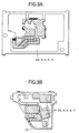
laser devices laser device 7 into three beams, 15 denotes a frame for the plate, and 16 denotes a frame for the case. - Figs. 3A and 3B are views which is used for describing the method of producing a resin package for a hybrid optical module according to the invention. Fig. 3A shows
lead frames 2 and 3 (4, 5, 6, 7) in which end portions have not yet been bent, and which are formed by punching out one thin copper plate by a press machine, and Fig. 3B shows the interior of a case in the state where the lead frames 2 and 3 (4, 5, 6, 7) are mounted into theresin package 1. The figure corresponds to the state where the hybrid optical module components shown in Fig. 2B are removed away. Namely, the hybrid optical module components shown in Fig. 2B are mounted on the lead frame shown in Figs. 3A and 3B. - The method of producing a resin package for a hybrid optical module according to the invention will be described. First, portions of the lead frames shown in Fig. 3A are vertically bent in accordance with a shape of the resin package. The portions of the lead frames are embedded into the
resin package 1, and a shaping process is then performed. The hybrid optical module components are housed in the completed resin package. Specifically, thelaser diodes - As described above, in the invention, components of a hybrid optical module are mounted on a lead frame made of a metal, and the frame is bent in a resin, thereby enhancing the mechanical strength of a resin package, and the surface area of the frame is increased so that the heat capacity in terms of a heat sink can be increased.
- When a pickup component, particularly a laser device is to be die-bonded onto a metal frame, a heat treatment is conducted. As described above, according to the invention, the metal frame is disposed independently from a metal frame onto which another laser device is to be die-bonded, and hence one laser device is not adversely affected by a process of die-bonding another laser device. Therefore, misalignment of the optical axis due to heat applied in the process of die-bonding can be suppressed. Since the metal frame is bent in the resin package, the strength of the resin package itself is enhanced. Furthermore, the surface area of the metal frame is increased, and the heat capacity in terms of a heat sink is therefore increased. Since heat is radiated to the outside via the frame led-out portion or the thin resin package, the heat radiation effect is improved.
Claims (6)
- A package structure for a hybrid optical module, comprising:components for detecting an optical signal, excluding an objective lens;a hollow resin package which houses said components for detecting an optical signal; anda metal frame a portion of which is mounted on said resin package, said components for detecting an optical signal being bonded onto said mounted portion, and another portion of which is vertically bent in accordance with a shape of said resin package and embedded into said resin package.
- A package structure for a hybrid optical module according to claim 1, wherein said components for detecting an optical signal constitute an optical pickup unit.
- A package structure for a hybrid optical module according to claim 1, wherein said metal frame is independently disposed for each of laser devices which are to be bonded.
- A package structure for a hybrid optical module according to claim 1, wherein said metal frame radiates heat via said resin package to a metal part disposed outside said resin package.
- A package structure for a hybrid optical module according to claim 1, wherein an end portion of said metal frame is led out from said resin package, and made in contact with a metal part disposed outside said resin package.
- A method of producing a package structure for a hybrid optical module, said package comprising: a hollow resin package which houses components for detecting an optical signal, excluding an objective lens; and a metal frame a portion of which is mounted on said resin package, and onto which said components for detecting an optical signal are to be bonded, wherein said method comprises the steps of:vertically bending another portion of said metal frame in accordance with a shape of said resin package;embedding said other portion of said metal frame into said resin package, and then performing a shaping process; andbonding said components for detecting an optical signal onto said portion of said metal frame.
Applications Claiming Priority (2)
| Application Number | Priority Date | Filing Date | Title |
|---|---|---|---|
| JP37516999A JP2001189027A (en) | 1999-12-28 | 1999-12-28 | Package structure of hybrid optical moduel, and its manufacturing method |
| JP37516999 | 1999-12-28 |
Publications (2)
| Publication Number | Publication Date |
|---|---|
| EP1113428A2 true EP1113428A2 (en) | 2001-07-04 |
| EP1113428A3 EP1113428A3 (en) | 2002-11-20 |
Family
ID=18505090
Family Applications (1)
| Application Number | Title | Priority Date | Filing Date |
|---|---|---|---|
| EP00311193A Withdrawn EP1113428A3 (en) | 1999-12-28 | 2000-12-14 | Package structure for a hybrid optical module and method of producing the same |
Country Status (3)
| Country | Link |
|---|---|
| US (1) | US6901092B2 (en) |
| EP (1) | EP1113428A3 (en) |
| JP (1) | JP2001189027A (en) |
Cited By (1)
| Publication number | Priority date | Publication date | Assignee | Title |
|---|---|---|---|---|
| EP1408489A2 (en) * | 2002-10-08 | 2004-04-14 | Pioneer Corporation | Pickup device |
Families Citing this family (4)
| Publication number | Priority date | Publication date | Assignee | Title |
|---|---|---|---|---|
| JP3587196B2 (en) | 2002-02-18 | 2004-11-10 | 船井電機株式会社 | Optical pickup |
| JP3909853B2 (en) * | 2004-04-26 | 2007-04-25 | 株式会社東芝 | Semiconductor laser device and semiconductor laser assembly |
| US11431146B2 (en) * | 2015-03-27 | 2022-08-30 | Jabil Inc. | Chip on submount module |
| DE102019119390A1 (en) * | 2019-07-17 | 2021-01-21 | OSRAM Opto Semiconductors Gesellschaft mit beschränkter Haftung | HOUSING FOR AN OPTOELECTRONIC COMPONENT, METHOD FOR MANUFACTURING A HOUSING FOR AN OPTOELECTRONIC COMPONENT, OPTOELECTRONIC COMPONENT AND METHOD FOR MANUFACTURING AN OPTOELECTRONIC COMPONENT |
Citations (2)
| Publication number | Priority date | Publication date | Assignee | Title |
|---|---|---|---|---|
| US5285062A (en) * | 1992-04-14 | 1994-02-08 | Hoetron, Inc. | Laser/detector hybrid with mirror source and diffracted return beam |
| EP0851414A2 (en) * | 1996-12-26 | 1998-07-01 | Sanyo Electric Co. Ltd | Optical pickup device and optical recording medium driving apparatus comprising the same |
Family Cites Families (2)
| Publication number | Priority date | Publication date | Assignee | Title |
|---|---|---|---|---|
| JPH0523563U (en) * | 1991-07-17 | 1993-03-26 | ソニー株式会社 | Semiconductor laser device |
| US6090642A (en) * | 1996-11-12 | 2000-07-18 | Rohm Co., Ltd. | Semiconductor laser diode assembly and method of manufacturing the same |
-
1999
- 1999-12-28 JP JP37516999A patent/JP2001189027A/en active Pending
-
2000
- 2000-12-14 EP EP00311193A patent/EP1113428A3/en not_active Withdrawn
- 2000-12-21 US US09/741,006 patent/US6901092B2/en not_active Expired - Fee Related
Patent Citations (2)
| Publication number | Priority date | Publication date | Assignee | Title |
|---|---|---|---|---|
| US5285062A (en) * | 1992-04-14 | 1994-02-08 | Hoetron, Inc. | Laser/detector hybrid with mirror source and diffracted return beam |
| EP0851414A2 (en) * | 1996-12-26 | 1998-07-01 | Sanyo Electric Co. Ltd | Optical pickup device and optical recording medium driving apparatus comprising the same |
Cited By (3)
| Publication number | Priority date | Publication date | Assignee | Title |
|---|---|---|---|---|
| EP1408489A2 (en) * | 2002-10-08 | 2004-04-14 | Pioneer Corporation | Pickup device |
| EP1408489A3 (en) * | 2002-10-08 | 2005-01-05 | Pioneer Corporation | Pickup device |
| US7137130B2 (en) | 2002-10-08 | 2006-11-14 | Pioneer Corporation | Pickup device with heat-radiating mechanism |
Also Published As
| Publication number | Publication date |
|---|---|
| JP2001189027A (en) | 2001-07-10 |
| EP1113428A3 (en) | 2002-11-20 |
| US6901092B2 (en) | 2005-05-31 |
| US20030031429A1 (en) | 2003-02-13 |
Similar Documents
| Publication | Publication Date | Title |
|---|---|---|
| US5925898A (en) | Optoelectronic transducer and production methods | |
| JP3386817B2 (en) | Opto-electronic converter and manufacturing method | |
| US6051848A (en) | Optical device packages containing an optical transmitter die | |
| US7948694B2 (en) | Apparatus for an optoelectronic device and componnent having an optoelectronic device and an apparatus | |
| EP1788631B1 (en) | Photonic device with integrated hybrid microlens array | |
| JP3318811B2 (en) | Semiconductor light emitting device package and method of manufacturing the same | |
| JPH09205251A (en) | Plastic molding apparatus for semiconductor laser | |
| WO2004001861A1 (en) | Photoelectric composite module and optical input/output device using the module as component element | |
| WO2016084833A1 (en) | Method for producing optical module | |
| US5590144A (en) | Semiconductor laser device | |
| US6829266B2 (en) | Optical semiconductor device increasing productivity and method of fabricating the same | |
| KR100446714B1 (en) | Semiconductor laser device, fabricating method thereof and optical pickup employing the semiconductor laser device | |
| US6901092B2 (en) | Package structure for a hybrid optical module and method of producing the same | |
| JP2003218447A (en) | Method of aligning parallel optics interconnect device | |
| US20060262820A1 (en) | Semiconductor laser device and optical pickup apparatus having the device | |
| CN100483872C (en) | Semiconductor laser device, method for manufacturing the same and optical pickup apparatus | |
| US20040071174A1 (en) | Semiconductor laser device containing laser driver and electronic equipment having the same | |
| US6414388B1 (en) | Light emitting/receiving element for optical pickup apparatus | |
| US5444726A (en) | Semiconductor laser device | |
| US6977951B2 (en) | Semiconductor laser apparatus and optical pickup apparatus using same | |
| JP3371954B2 (en) | Optical / Electric hybrid module | |
| CN113985533A (en) | Photonic semiconductor device and method for manufacturing the same | |
| US7109524B2 (en) | Metal carrier (leadframe) for receiving and contact-connecting electrical and/or optoelectronic components | |
| EP1115112B1 (en) | Hybrid optical module | |
| JP4439313B2 (en) | Manufacturing method of optical module |
Legal Events
| Date | Code | Title | Description |
|---|---|---|---|
| PUAI | Public reference made under article 153(3) epc to a published international application that has entered the european phase |
Free format text: ORIGINAL CODE: 0009012 |
|
| AK | Designated contracting states |
Kind code of ref document: A2 Designated state(s): AT BE CH CY DE DK ES FI FR GB GR IE IT LI LU MC NL PT SE TR |
|
| AX | Request for extension of the european patent |
Free format text: AL;LT;LV;MK;RO;SI |
|
| PUAL | Search report despatched |
Free format text: ORIGINAL CODE: 0009013 |
|
| AK | Designated contracting states |
Kind code of ref document: A3 Designated state(s): AT BE CH CY DE DK ES FI FR GB GR IE IT LI LU MC NL PT SE TR |
|
| AX | Request for extension of the european patent |
Free format text: AL;LT;LV;MK;RO;SI |
|
| RIC1 | Information provided on ipc code assigned before grant |
Free format text: 7G 11B 7/12 A, 7H 01L 33/00 B, 7G 11B 7/22 B, 7H 01L 25/16 B, 7H 01L 31/0203 B |
|
| 17P | Request for examination filed |
Effective date: 20030502 |
|
| AKX | Designation fees paid |
Designated state(s): DE FR GB |
|
| 17Q | First examination report despatched |
Effective date: 20050318 |
|
| STAA | Information on the status of an ep patent application or granted ep patent |
Free format text: STATUS: THE APPLICATION IS DEEMED TO BE WITHDRAWN |
|
| 18D | Application deemed to be withdrawn |
Effective date: 20070703 |