EP1113428A2 - Package structure for a hybrid optical module and method of producing the same - Google Patents
Package structure for a hybrid optical module and method of producing the same Download PDFInfo
- Publication number
- EP1113428A2 EP1113428A2 EP00311193A EP00311193A EP1113428A2 EP 1113428 A2 EP1113428 A2 EP 1113428A2 EP 00311193 A EP00311193 A EP 00311193A EP 00311193 A EP00311193 A EP 00311193A EP 1113428 A2 EP1113428 A2 EP 1113428A2
- Authority
- EP
- European Patent Office
- Prior art keywords
- resin package
- package
- optical module
- metal frame
- components
- Prior art date
- Legal status (The legal status is an assumption and is not a legal conclusion. Google has not performed a legal analysis and makes no representation as to the accuracy of the status listed.)
- Withdrawn
Links
Images

Classifications
-
- G—PHYSICS
- G11—INFORMATION STORAGE
- G11B—INFORMATION STORAGE BASED ON RELATIVE MOVEMENT BETWEEN RECORD CARRIER AND TRANSDUCER
- G11B7/00—Recording or reproducing by optical means, e.g. recording using a thermal beam of optical radiation by modifying optical properties or the physical structure, reproducing using an optical beam at lower power by sensing optical properties; Record carriers therefor
- G11B7/12—Heads, e.g. forming of the optical beam spot or modulation of the optical beam
- G11B7/22—Apparatus or processes for the manufacture of optical heads, e.g. assembly
-
- H—ELECTRICITY
- H01—ELECTRIC ELEMENTS
- H01S—DEVICES USING THE PROCESS OF LIGHT AMPLIFICATION BY STIMULATED EMISSION OF RADIATION [LASER] TO AMPLIFY OR GENERATE LIGHT; DEVICES USING STIMULATED EMISSION OF ELECTROMAGNETIC RADIATION IN WAVE RANGES OTHER THAN OPTICAL
- H01S5/00—Semiconductor lasers
- H01S5/02—Structural details or components not essential to laser action
- H01S5/022—Mountings; Housings
- H01S5/023—Mount members, e.g. sub-mount members
- H01S5/0232—Lead-frames
-
- H—ELECTRICITY
- H10—SEMICONDUCTOR DEVICES; ELECTRIC SOLID-STATE DEVICES NOT OTHERWISE PROVIDED FOR
- H10W—GENERIC PACKAGES, INTERCONNECTIONS, CONNECTORS OR OTHER CONSTRUCTIONAL DETAILS OF DEVICES COVERED BY CLASS H10
- H10W90/00—Package configurations
-
- H—ELECTRICITY
- H01—ELECTRIC ELEMENTS
- H01S—DEVICES USING THE PROCESS OF LIGHT AMPLIFICATION BY STIMULATED EMISSION OF RADIATION [LASER] TO AMPLIFY OR GENERATE LIGHT; DEVICES USING STIMULATED EMISSION OF ELECTROMAGNETIC RADIATION IN WAVE RANGES OTHER THAN OPTICAL
- H01S5/00—Semiconductor lasers
- H01S5/02—Structural details or components not essential to laser action
- H01S5/022—Mountings; Housings
- H01S5/023—Mount members, e.g. sub-mount members
- H01S5/0231—Stems
-
- H—ELECTRICITY
- H01—ELECTRIC ELEMENTS
- H01S—DEVICES USING THE PROCESS OF LIGHT AMPLIFICATION BY STIMULATED EMISSION OF RADIATION [LASER] TO AMPLIFY OR GENERATE LIGHT; DEVICES USING STIMULATED EMISSION OF ELECTROMAGNETIC RADIATION IN WAVE RANGES OTHER THAN OPTICAL
- H01S5/00—Semiconductor lasers
- H01S5/40—Arrangement of two or more semiconductor lasers, not provided for in groups H01S5/02 - H01S5/30
- H01S5/4025—Array arrangements, e.g. constituted by discrete laser diodes or laser bar
- H01S5/4087—Array arrangements, e.g. constituted by discrete laser diodes or laser bar emitting more than one wavelength
-
- H—ELECTRICITY
- H10—SEMICONDUCTOR DEVICES; ELECTRIC SOLID-STATE DEVICES NOT OTHERWISE PROVIDED FOR
- H10H—INORGANIC LIGHT-EMITTING SEMICONDUCTOR DEVICES HAVING POTENTIAL BARRIERS
- H10H20/00—Individual inorganic light-emitting semiconductor devices having potential barriers, e.g. light-emitting diodes [LED]
- H10H20/80—Constructional details
- H10H20/85—Packages
- H10H20/857—Interconnections, e.g. lead-frames, bond wires or solder balls
Definitions
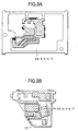
- the frame led-out portion 10 is requested not to impede a rotation mechanism for adjusting a grating. Therefore, the frame led-out portion 10 must be placed so as to be rotatable in balance.
- the frame led-out portion is bent at a midpoint.
- the embodiment has the structure in which the frame led-out portion 10 is made in contact with a heat sink disposed outside the resin package 1 so as to radiate heat to the external. In this case, however, it is not necessary to make the frame led-out portion in direct contact with the heat sink. Even when direct contact is not made, the frame led-out portion can contribute to heat radiation through a thin resin layer.
Landscapes
- Physics & Mathematics (AREA)
- Optics & Photonics (AREA)
- Condensed Matter Physics & Semiconductors (AREA)
- General Physics & Mathematics (AREA)
- Electromagnetism (AREA)
- Semiconductor Lasers (AREA)
- Led Device Packages (AREA)
- Optical Head (AREA)
Abstract
Description
Claims (6)
- A package structure for a hybrid optical module, comprising:components for detecting an optical signal, excluding an objective lens;a hollow resin package which houses said components for detecting an optical signal; anda metal frame a portion of which is mounted on said resin package, said components for detecting an optical signal being bonded onto said mounted portion, and another portion of which is vertically bent in accordance with a shape of said resin package and embedded into said resin package.
- A package structure for a hybrid optical module according to claim 1, wherein said components for detecting an optical signal constitute an optical pickup unit.
- A package structure for a hybrid optical module according to claim 1, wherein said metal frame is independently disposed for each of laser devices which are to be bonded.
- A package structure for a hybrid optical module according to claim 1, wherein said metal frame radiates heat via said resin package to a metal part disposed outside said resin package.
- A package structure for a hybrid optical module according to claim 1, wherein an end portion of said metal frame is led out from said resin package, and made in contact with a metal part disposed outside said resin package.
- A method of producing a package structure for a hybrid optical module, said package comprising: a hollow resin package which houses components for detecting an optical signal, excluding an objective lens; and a metal frame a portion of which is mounted on said resin package, and onto which said components for detecting an optical signal are to be bonded, wherein said method comprises the steps of:vertically bending another portion of said metal frame in accordance with a shape of said resin package;embedding said other portion of said metal frame into said resin package, and then performing a shaping process; andbonding said components for detecting an optical signal onto said portion of said metal frame.
Applications Claiming Priority (2)
| Application Number | Priority Date | Filing Date | Title |
|---|---|---|---|
| JP37516999A JP2001189027A (en) | 1999-12-28 | 1999-12-28 | Package structure of hybrid optical module and method of manufacturing the same |
| JP37516999 | 1999-12-28 |
Publications (2)
| Publication Number | Publication Date |
|---|---|
| EP1113428A2 true EP1113428A2 (en) | 2001-07-04 |
| EP1113428A3 EP1113428A3 (en) | 2002-11-20 |
Family
ID=18505090
Family Applications (1)
| Application Number | Title | Priority Date | Filing Date |
|---|---|---|---|
| EP00311193A Withdrawn EP1113428A3 (en) | 1999-12-28 | 2000-12-14 | Package structure for a hybrid optical module and method of producing the same |
Country Status (3)
| Country | Link |
|---|---|
| US (1) | US6901092B2 (en) |
| EP (1) | EP1113428A3 (en) |
| JP (1) | JP2001189027A (en) |
Cited By (1)
| Publication number | Priority date | Publication date | Assignee | Title |
|---|---|---|---|---|
| EP1408489A3 (en) * | 2002-10-08 | 2005-01-05 | Pioneer Corporation | Pickup device |
Families Citing this family (5)
| Publication number | Priority date | Publication date | Assignee | Title |
|---|---|---|---|---|
| JP3529046B2 (en) | 2001-08-17 | 2004-05-24 | 船井電機株式会社 | Optical pickup |
| JP3587196B2 (en) | 2002-02-18 | 2004-11-10 | 船井電機株式会社 | Optical pickup |
| JP3909853B2 (en) * | 2004-04-26 | 2007-04-25 | 株式会社東芝 | Semiconductor laser device and semiconductor laser assembly |
| US11431146B2 (en) * | 2015-03-27 | 2022-08-30 | Jabil Inc. | Chip on submount module |
| DE102019119390A1 (en) * | 2019-07-17 | 2021-01-21 | OSRAM Opto Semiconductors Gesellschaft mit beschränkter Haftung | HOUSING FOR AN OPTOELECTRONIC COMPONENT, METHOD FOR MANUFACTURING A HOUSING FOR AN OPTOELECTRONIC COMPONENT, OPTOELECTRONIC COMPONENT AND METHOD FOR MANUFACTURING AN OPTOELECTRONIC COMPONENT |
Family Cites Families (4)
| Publication number | Priority date | Publication date | Assignee | Title |
|---|---|---|---|---|
| JPH0523563U (en) * | 1991-07-17 | 1993-03-26 | ソニー株式会社 | Semiconductor laser device |
| US5285062A (en) * | 1992-04-14 | 1994-02-08 | Hoetron, Inc. | Laser/detector hybrid with mirror source and diffracted return beam |
| US6090642A (en) * | 1996-11-12 | 2000-07-18 | Rohm Co., Ltd. | Semiconductor laser diode assembly and method of manufacturing the same |
| EP0851414A3 (en) * | 1996-12-26 | 2000-09-27 | Sanyo Electric Co. Ltd | Optical pickup device and optical recording medium driving apparatus comprising the same |
-
1999
- 1999-12-28 JP JP37516999A patent/JP2001189027A/en active Pending
-
2000
- 2000-12-14 EP EP00311193A patent/EP1113428A3/en not_active Withdrawn
- 2000-12-21 US US09/741,006 patent/US6901092B2/en not_active Expired - Fee Related
Cited By (2)
| Publication number | Priority date | Publication date | Assignee | Title |
|---|---|---|---|---|
| EP1408489A3 (en) * | 2002-10-08 | 2005-01-05 | Pioneer Corporation | Pickup device |
| US7137130B2 (en) | 2002-10-08 | 2006-11-14 | Pioneer Corporation | Pickup device with heat-radiating mechanism |
Also Published As
| Publication number | Publication date |
|---|---|
| US20030031429A1 (en) | 2003-02-13 |
| EP1113428A3 (en) | 2002-11-20 |
| US6901092B2 (en) | 2005-05-31 |
| JP2001189027A (en) | 2001-07-10 |
Similar Documents
| Publication | Publication Date | Title |
|---|---|---|
| US6051848A (en) | Optical device packages containing an optical transmitter die | |
| US5925898A (en) | Optoelectronic transducer and production methods | |
| US5825054A (en) | Plastic-molded apparatus of a semiconductor laser | |
| JP3318811B2 (en) | Semiconductor light emitting device package and method of manufacturing the same | |
| EP1788631B1 (en) | Photonic device with integrated hybrid microlens array | |
| WO2004001861A1 (en) | Photoelectric composite module and optical input/output device using the module as component element | |
| CN1228861C (en) | Compound optical element and light receiving element device | |
| JP4643891B2 (en) | Positioning method for parallel optical system connection device | |
| US5590144A (en) | Semiconductor laser device | |
| US7184453B2 (en) | Semiconductor laser device containing laser driver and electronic equipment having the same | |
| US6901092B2 (en) | Package structure for a hybrid optical module and method of producing the same | |
| US6829266B2 (en) | Optical semiconductor device increasing productivity and method of fabricating the same | |
| US6414388B1 (en) | Light emitting/receiving element for optical pickup apparatus | |
| US7020174B2 (en) | Laser diode module for optical communication | |
| US5444726A (en) | Semiconductor laser device | |
| CN100414792C (en) | Semiconductor laser device and optical pickup device having same | |
| EP1115112B1 (en) | Hybrid optical module | |
| JP4439313B2 (en) | Manufacturing method of optical module | |
| GB2310749A (en) | Bar code reading optical apparatus | |
| KR20050043219A (en) | Optical pickup module and manufacturing method thereof | |
| CN113985533A (en) | Photonic semiconductor device and method for manufacturing the same | |
| JP2005190520A (en) | Optical head device | |
| EP0568830B1 (en) | Semiconductor laser device | |
| US20070029472A1 (en) | Light emitting and receiving integrated device and optical disk apparatus | |
| JP3520621B2 (en) | Optical pickup and optical pickup for phase change optical disk |
Legal Events
| Date | Code | Title | Description |
|---|---|---|---|
| PUAI | Public reference made under article 153(3) epc to a published international application that has entered the european phase |
Free format text: ORIGINAL CODE: 0009012 |
|
| AK | Designated contracting states |
Kind code of ref document: A2 Designated state(s): AT BE CH CY DE DK ES FI FR GB GR IE IT LI LU MC NL PT SE TR |
|
| AX | Request for extension of the european patent |
Free format text: AL;LT;LV;MK;RO;SI |
|
| PUAL | Search report despatched |
Free format text: ORIGINAL CODE: 0009013 |
|
| AK | Designated contracting states |
Kind code of ref document: A3 Designated state(s): AT BE CH CY DE DK ES FI FR GB GR IE IT LI LU MC NL PT SE TR |
|
| AX | Request for extension of the european patent |
Free format text: AL;LT;LV;MK;RO;SI |
|
| RIC1 | Information provided on ipc code assigned before grant |
Free format text: 7G 11B 7/12 A, 7H 01L 33/00 B, 7G 11B 7/22 B, 7H 01L 25/16 B, 7H 01L 31/0203 B |
|
| 17P | Request for examination filed |
Effective date: 20030502 |
|
| AKX | Designation fees paid |
Designated state(s): DE FR GB |
|
| 17Q | First examination report despatched |
Effective date: 20050318 |
|
| STAA | Information on the status of an ep patent application or granted ep patent |
Free format text: STATUS: THE APPLICATION IS DEEMED TO BE WITHDRAWN |
|
| 18D | Application deemed to be withdrawn |
Effective date: 20070703 |