EP1113383A2 - Enhanced fingerprint detection - Google Patents
Enhanced fingerprint detection Download PDFInfo
- Publication number
- EP1113383A2 EP1113383A2 EP00311521A EP00311521A EP1113383A2 EP 1113383 A2 EP1113383 A2 EP 1113383A2 EP 00311521 A EP00311521 A EP 00311521A EP 00311521 A EP00311521 A EP 00311521A EP 1113383 A2 EP1113383 A2 EP 1113383A2
- Authority
- EP
- European Patent Office
- Prior art keywords
- capacitance
- voltage
- cell
- finger
- capacitor
- Prior art date
- Legal status (The legal status is an assumption and is not a legal conclusion. Google has not performed a legal analysis and makes no representation as to the accuracy of the status listed.)
- Withdrawn
Links
Images




Classifications
-
- A—HUMAN NECESSITIES
- A61—MEDICAL OR VETERINARY SCIENCE; HYGIENE
- A61B—DIAGNOSIS; SURGERY; IDENTIFICATION
- A61B5/00—Measuring for diagnostic purposes; Identification of persons
- A61B5/117—Identification of persons
- A61B5/1171—Identification of persons based on the shapes or appearances of their bodies or parts thereof
- A61B5/1172—Identification of persons based on the shapes or appearances of their bodies or parts thereof using fingerprinting
-
- G—PHYSICS
- G06—COMPUTING OR CALCULATING; COUNTING
- G06V—IMAGE OR VIDEO RECOGNITION OR UNDERSTANDING
- G06V40/00—Recognition of biometric, human-related or animal-related patterns in image or video data
- G06V40/10—Human or animal bodies, e.g. vehicle occupants or pedestrians; Body parts, e.g. hands
- G06V40/12—Fingerprints or palmprints
- G06V40/13—Sensors therefor
- G06V40/1306—Sensors therefor non-optical, e.g. ultrasonic or capacitive sensing
Definitions
- This invention is related to fingerprint pattern recognition, and more particularly, to enhanced fingerprint pattern sensing circuit and method.
- Capacitive sensors to detect a fingerprint pattern are currently well known. There are a number of patents which describe capacitive sensors for determining the pattern of ridges and valleys in a person's fingerprint.
- U.S. Patent No. 4,353,056 describes a capacitive fingerprint sensor which has a sensing surface for receiving a fingerprint and sensing the ridges and valleys of the skin using an array of small capacitors.
- U.S. Patent No. 5,325,442 also describes a fingerprint sensing and recognition circuit using a plurality of capacitors arranged in rows and columns.
- Some capacitive sensors operate using two or more plates in silicon with a negative feedback as shown in Figures 1 and 2, taken from U.S. Patent No. 5,973,623.
- the finger of the user changes the capacitance that exists between the two plates in silicon.
- a negative feedback circuit is used in the detection of whether a ridge or a valley is present in the fingerprint.
- Some capacitive sensors operate using a single capacitor plate in silicon per sensor cell. This type of sensor is shown in U.S. Patent No. 5,325,442. Figures 3 and 4 are prior art. Figures from this patent illustrate a single capacitive plate 14 and a switching device 16 to access the sensor cell. The finger of the user provides the other plate of the capacitor. The value of the capacitor is then sensed to determine the presence of a ridge or a valley.
- One of the problems with the prior art capacitive fingerprint sensors is their level of sensitivity to distinguish a ridge from a valley.
- the difficulty of obtaining a good fingerprint pattern through capacitive sensing can vary from individual to individual. With some persons, depending upon their skin characteristics the pattern can be much more difficult to obtain than from other persons. It is therefore preferred to have an enhanced method of capacitive sensing which provides more uniform sensitivity from one individual to another.
- a capacitive fingerprint sensing device which changes the voltage on the body of the individual whose fingerprint pattern is being sensed.
- the person's body is also placed in contact with an electrically conductive connector.
- the voltage on the electrical connector changes, which changes the voltage on the person's body.
- the fingerprint pattern is a second part of the sensing circuit, rather than being solely a plate of a capacitor, it is now an input as well.
- the electrical effect of a voltage change on a person's finger is different at a ridge than at a valley in the fingerprint sensing circuit.
- the input capacitance to the sensing circuit is variable, depending upon whether a ridge or a valley is present.
- the sensing circuit also detects a change in its own capacitance based on the presence of a ridge or a valley.
- the person's body acts as the input capacitor to provide a variable charge transfer for the input capacitance and at the same time performs the function of being a variable capacitor value for the capacitive sensor.
- the finger is thus performing the dual function of providing the variable charge transfer while also providing the variable capacitance to be sensed.
- the effect of performing both functions effectively multiplies the measurable effects of having a ridge or a valley at each local sensor and thus the sensing is significantly enhanced in recognizing and distinguishing the difference between a ridge and a valley.
- the electrical connection to the person's body can be made by any number of acceptable techniques.
- an electrical contact is provided to the person's finger while it is placed on the fingerprint sensor pad.
- a logic control circuit connected to the electrical conductor places a step voltage on the electrical conductor according to a preset timing sequence in conjunction with the timing of the sensing.
- the voltage change is placed on the person's body by a capacitive transfer.
- a large plate capacitor in the silicon provides one plate to transfer charge to the finger to provide the change in voltage while the sensing occurs.
- the voltage change can be coupled to the body of the user either via another finger or some other appendage.
- the connector can be in contact with the other hand of the person, their arm or any other acceptable portion of the body since all that is required is to place a change in charge on the person's body in order to obtain the enhanced capacitive sensing capability.
- the invention can be used with sensor cells of the type having one capacitive plate in silicon and the finger providing the other plate, or with the type using multiple capacitor plates in silicon and the finger being a conductor that modifies their relative capacitance.
- the fingerprint or sensor circuit includes a negative feedback amplifier having the two plates of a capacitor in silicon with a field therebetween.
- the field between the two plates is varied by the user's finger, whether ridge or valley.
- the effect of having a valley is that the sense capacitance will be greater than a greater ridge.
- the capacitance is reduced, as compared to a valley.
- the input capacitance will decrease with the greater distance of the skin from the sensor, such as is present at a valley.
- Figure 1 is a schematic representation of a fingerprint sensor according to the prior art.
- Figure 2 is an electrical schematic representation of an individual cell of the fingerprint sensor of Figure 1 according to the prior art.
- Figure 3 is a schematic representation of a fingerprint sensor circuit according to different prior art embodiment.
- Figure 4 is an electrical schematic of the fingerprint sensor from Figure 3.
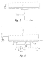
- Figure 5 is an electrical schematic of a fingerprint sensor according to the present invention.
- Figure 6 is a schematic representation of a fingerprint sensor according to principles of the present invention.
- Figure 7 is an electrical schematic of an alternative embodiment of a fingerprint sensor according to principles of the present invention.
- Figure 8 is an electrical schematic of a fingerprint according to the present invention.
- Figure 9 is an electrical schematic of a plurality of cells while sensing a fingerprint ridge and valley pattern according to principles of the present invention.
- Figure 10 is an electrical equivalent circuit showing the electrical interaction between various equivalent electrical components according to principles of the present invention.
- Figure 11 is a top view of a housing containing a sensor according to the present invention.
- Figure 12 is a partial cross-sectional view of the substrate of Figure 7 taken along the lines 12.
- Figure 13 is a partial cross-sectional view of an alternative substrate and housing containing the invention.
- Figure 14 is a partial cross-sectional view of an alternative substrate and housing of the present invention.
- Figure 15 is a side view of a further alternative embodiment to place a voltage change on the finger of the user.
- Figure 16 is an electrical schematic of the circuit according to principles of the present invention.
- Figure 1 illustrates a substrate 1 having a plurality of sensor cells 2 thereon.
- the sensor cells 2 are in the form of an array 3 and organized to sense a fingerprint pattern of a finger which is placed on top of the substrate.
- the array 3 is driven by horizontal scan electronics 5 and also by vertical scan electronics 6 so that each individual cell 2 is selected on a known timing sequence under control of the controller 7.
- each sensor cell 2 includes electronics for sensing the presence or absence of a ridge or a valley of a fingerprint pattern for a finger which is placed on top of the substrate 1.
- the controller 7 includes a power supply circuit 120 which receives power from a power source 95.
- Each sensing cell 2 provides an output on line 17 of each individual column.
- the output is provided on the chip bus 19 which is provided to an output amplifier 8 and provided to the output of the sensor array 3 at terminal 10.
- the output of the sensor array 3 at terminal 10 is provided to fingerprint pattern recognition electronics which organizes the signal into a fingerprint pattern and compares it to other fingerprint patterns to perform recognition of the fingerprint pattern which is placed thereon.
- the specific details of the array 3 and interaction between the controller 7 to provide fingerprint pattern recognition is described in U.S. Patent No. 5,973,623, which is incorporated herein by reference.
- the fingerprint pattern recognition may also be obtained and performed by any acceptable technique of the many other patents and publications which are available to those of skill in the art today.
- Figure 2 illustrates the electronics of a single sensor cell 2 which is acceptable for use in sensing the presence or absence of a ridge or valley.
- the specific electronics for the cell 2 are provided as only one example by which the cell can be constructed. Other acceptable techniques may also be used since the electronics of the individual cell are provided as an example only.
- the cell 2 includes a dielectric layer 11 onto which a person's finger is placed.
- the dielectric layer 11 has a top surface 125 which comes in direct contact with the person's scanned finger 18.
- the finger 18 will have a ridge or a valley at the position in which it comes in contact with the cell 2, an example shown for Figure 2 including having a ridge thereon so that it is pressed against the substrate 11 and in contact with surface 125.
- the dielectric layer 11 has a thickness D as shown in Figure 2.
- a capacitor having plates 24 and 23 is against the back surface of the dielectric layer 11.
- the input plate of the cluster 24 is connected to the input terminal of an inverting amplifier 13 and the output plate 23 is connected to the output of the inverting amplifier 13.
- a reset switch 19 is closed when sensing is not being performed to reset the inverting amplifier 13 to a known state.
- a capacitor 20 provides a step voltage N as applied through V ref at terminal 21.
- the capacitor C in is of a known value to provide a known charge to the input node 16 of inverting amplifier 13.
- Figure 3 illustrates another acceptable sensor cell 2 which may be used according to principles of the present invention.
- the particular sensor cell 2 is known from prior art U.S. Patent No. 5,555,555, to Knapp, which is hereby incorporated herein by reference.
- the sensor cell to Knapp according to the description in his own patent includes a sensor electronics and sensor cell and a capacitor plate C.
- the capacitance value of a capacitor varies with the distance of the plates from each other. In a fingerprint pattern sensor, the fingerprint, whether a ridge or a valley, acts as a plate of the capacitor. The distance varies in the fingerprint, small for a ridge and large for a valley, the capacitance is also different and can be sensed. In a multiple plate sensor, such as Figure 2 shows, the capacitance value also varies depending upon the fringing effect from other conductors adjacent the two capacitor plates as described by the later equations herein.
- the sensor cell 2 provides an output voltage which is based on the presence of a ridge or a valley in finger 18 which is directly over the cell 2.
- V out In many sensors, particularly the single plate type, it is desired to measure V out directly, with each cell 2 providing a different V out voltage from every other cell 2. According to other types of sensor cells 2, it is desirable to measure a change in V out from a starting point or a known reset of reference value, such as is done for the sensor cell 2 as shown in Figure 2.
- ⁇ V out ⁇ q C s in which ⁇ V out equals the change in voltage on terminal 17
- ⁇ q equals the change in charge on the capacitance
- C s is the capacitance being sensed, namely, the capacitance of the capacitor composed of plates 24 and 23 with the conductor 18 of the finger adjacent thereto whether a ridge or a valley. The presence of a ridge and a valley will cause a change in the capacitance of capacitor composed of plates 24 and 23.
- the presence of a ridge near sensor cell 2 will cause the capacitance being sensed to be reduced, since having a conductor adjacent the plates of the capacitor will ground some of the field lines between the capacitance plates.
- the sensed capacitance c s will be greater than that of a ridge since a valley has a conductor spaced farther from the cell 2.
- the reduction of capacitance may be zero though, in a real sense, even a valley may cause some slight reduction in the capacitance value.
- a circuit which takes advantage of the variations in the capacitance interaction based on the presence of either a ridge or a valley over the sensor cell 2 as will now be explained.
- Figure 6 illustrates one example of fingerprint sensing according to principles of the present invention.
- the sensor cell as shown in Figure 6 is only one example.
- the same invention is applicable to the single plate sensor cell of Figure 5 as explained herein as will be clear from the technical discussion.
- an electrical conductor 21 is connected to the body of the person whose fingerprint is being sensed.
- Electrical conductor 21 has a terminal 19 connected to a variable voltage supply ⁇ V in .
- the ⁇ V in is directly controlled in a timing sequence with electronic controller 7 to place a known change of voltage on the body and thus on the finger 18 in conjunction with the timing of sensing in each individual cell 2.
- the ⁇ V in will normally be a low value and, once sensing has begun will undergo step voltage to high value as shown by the signal wave 23 applied to the terminal ⁇ V in .
- the cell 2 After the sensing has occurred while the voltage ⁇ V in is at a high value then the cell 2 will be reset and the electrical conductor 21 will be returned to a low value so as to place the both the cell and the body in a reset mode in preparation for the next sensing cycle at which time ⁇ V in undergoes another step value upwards as shown by signal wave 23 in Figure 4.
- the step on ⁇ V in is timed in conjunction with the timing sequence of a clock signal ⁇ r which controls the opening and closing of switch 19. Namely, switch 19 is opened and after which the ⁇ V in undergoes the step function upwards so that the change in voltage ⁇ V in occurs when switch 19 is open. This creates a change on input node 25 to inverting amplifier 13 which creates a change in voltage on V out corresponding to ⁇ V out as discussed in the prior equations.
- FIG. 7 illustrates an alternative embodiment for a circuit according to principles of the present invention.
- a separate capacitor C f This provided a separate capacitor C f 27 which acts as a compensation capacitor or filter to the input node 25 to enhance and further increase the sensitivity.
- One plate of the capacitor C f is connected to the sense node 25 whereas the other plate of the capacitor is connected to a voltage source V c representing a compensation voltage.
- the voltage source V c also undergoes a change in voltage according to a known timing sequence and thus is shown as a ⁇ V c .
- the compensation voltage ⁇ V c undergoes a change in voltage which is exactly opposite that of ⁇ V in which is placed on the body.
- the signals ⁇ V in and ⁇ V c will normally be the inverse of each other such that when ⁇ V in undergoes a step function up, ⁇ V c will undergo step down:
- the magnitude and absolute direction of ⁇ V in and ⁇ V c is not so important as there being a change in voltage.
- the ⁇ V in shown in Figure 7 as undergoing a step function from a low signal to a high signal could, of course, undergo a step function from a low signal to a negative voltage, or from a high signal to a low signal to place the change in voltage on the finger 18.
- ⁇ V in can transition from low to high and from high to low, respectively, as shown in Figure 7 or can transition from high to low and from low to high, respectively, in order to provide the enhanced sensing according to principles of the present invention.
- the terminal 19 has applied thereto a change in voltage ⁇ V in and the terminal 29 also as applied thereto, a change in voltage ⁇ V c as previously described with respect to Figure 7.
- the impedance of the body 31 is characterized according to a number of different electrical equations, and is sufficient for purposes of the invention to view the overall impedance of the body whether composed of various capacitors, resistors or combinations thereof as the overall body impedance 31.
- the body also has a resistance to ground 33 which varies greatly from one person to another. As can be appreciated, in some embodiments the resistance to ground 33 characterized by resistor R g can be extremely large.
- the resistance R g will approach infinity so that in fact, the person is not grounded and, from an electrical voltage potential, the voltage on the body is floating.
- the resistance R g will be extremely small, because the body is connected directly to ground.
- the value for resistor R g may vary from one circumstance to another.
- Figure 9 shows two sensor cells 2 which are spaced from each other in different parts of array 3.
- the first cell 2 is shown with a ridge directly over the cell 2
- the second cell is shown with a valley over the cell 2 so that the differences in operation can be easily explained and understood.
- the distance between the skin is D 1 since the skin is in direct contact with the upper surface 125 of the dielectric layer 11.
- the effect of the ridge 18 is to reduce the value of the capacitance between plates 24 and 23 of the negative feedback amplifier 13.
- the capacitance between plates 24 and 23 is shown by the field lines 35 with fewer field lines illustrated in a reduction in the capacitance value.
- the input capacitance which is an active part of the sensing circuit, also has effect on the sensor cell 2.
- the input capacitor C in is also variable as coming from the body will go high at a ridge, as compared to a valley.
- C in has its maximum value at a ridge.
- C s goes down at a ridge, namely C s will have its minimum value at a ridge.
- the recognition that a ridge has an opposite effect on the two capacitance values, namely that it causes a decrease in the sense capacitance C s and an increase in the input capacitance is a principle of the present invention, which is then used to provide enhanced sensitivity for fingerprint pattern recognition.
- C in and C s are a ratio which is used for changing the output value V out .
- the body itself is used as the input capacitor as well as for the sense capacitor so that enhanced sensitivity is obtained, as will be explained with respect to the following equations.
- the value C in was fixed so that ⁇ V in x C in created a step function change of the amount of charge applied at node 16.
- the value Q in was always a known value for each cell and did not vary.
- the body is used for C in , when the body undergoes a step function ⁇ V in the amount of charge provided at each individual cell will be different from that provided to other cells since the value locally at the individual cell will be different for each capacitor C in . Accordingly, the amount of charge transferred to the input node 25 will also vary for each individual cell.
- the actual local capacitance of each individual cell will not be precisely known, and will vary over a wide range.
- the finger 18 is separated by a distance d 2 from the upper surface 125 of dielectric layer 11. Since a valley is curved, the actual shape may vary from a normal distance d 2 to a maximum distance and an intermediate distance. Taking the case in which the valley is quite large, there will be no interference between the capacitive field lines 35 that extend between the plates 24 and 23 of the feedback capacitor to the negative amplifier 13. In particular, all of the field lines 35 which existed between plates 24 and 23 still exist when the valley is adjacent the cell such that it does not interfere with the capacitance value in any way. The capacitance value C s is therefore at a maximum value for the presence of a valley. On the other hand, the input capacitance is represented by field lines 37 is at a minimum value.
- the input capacitance is very small, and for a large valley is at a minimum value. This is to be compared with the ridge of cell 2a at which the input capacitance was large and there were a large number of field lines 37, as shown.
- Figure 10 illustrates an electrical schematic showing equivalent circuit of some components which will exist under normal operating conditions.
- the input node 25 will have a parasitic capacitor 41 coupled thereto.
- output node 17 will have a parasitic capacitor 43 coupled thereto.
- These parasitic capacitors C p will have an effect on the electrical operation of the circuit.
- the electrical equivalent of the negative feedback amplifier 13 is a simple inverter 13, as shown in Figure 7, assuming, the situation of an ideal negative amplifier with infinite gain. In this situation, a number of field lines 35 extend between plates 24 and 23 of the capacitor, which provides the negative feedback from the output 17 to the input 25.
- the field lines 37 represent the value and strength of the input capacitance provided from the body being used as the input capacitor.
- ⁇ V in and ⁇ V c are inverse signals of each other, such that they vary exactly the opposite in timing and in magnitude.
- the step voltage ⁇ V in is connected to capacitance of the body via Z BODY, as previously shown with respect to Figure 6.
- the plate 43 of the capacitance of the body has a different effect than when the conductor of the body is spaced farther from the plates 24 and 23.
- the input field lines 37 are significantly increased so that the capacitance 43 of the body and the overall body conductor has the effect of causing an increase in the input capacitance at node 25.
- the body capacitance 43 has a valley adjacent the cell 2, it will have a reduced input capacitance represented by reduced field lines 37 and an increased capacitance between plates 24 and 23, since the valley does not interfere with the field lines 35, again shown in Figure 6.
- the parasitic capacitance 41 and 43 thus have an overall reduced effect on the circuit.
- Figures 11 and 12 illustrate one acceptable technique for placing the change in voltage ⁇ V in on the human body while the fingerprint sensing is occurring.
- the substrate 1 is included within a housing 60. Positioned on the face of the substrate 1 are a plurality of electrical conductors 30,'as shown in Figures 8 and 9.
- the conductors 30 and 31 are electrically conductive strips formed in the upper surface of the substrate 1. In particular, these electrical conductors will be in direct electrical contact with the finger 18 of the user that is placed on the substrate 1.
- the electrical conductors 30 and 31 have applied thereto the step voltage ⁇ V in or, a grounding voltage, depending on the timing of the sense operation and the location of the cell being sensed relative to the electrical conductors 30, 31.
- One set of conductors 30 has the step voltage ⁇ V in applied thereto so as to place ⁇ V in on the body, according to the timing sequences previously described.
- the other conductors are grounded, so as to ground the portion of the finger 18 which is not adjacent the cell being sensed. In this case, the resistance to ground 33 as shown in Figure 6 is reduced to 0.
- each of the grid of wires is the array 3 composed of a plurality of sensor cells 2.
- the grid of wires which is adjacent that particular cell will be connected to ⁇ V in by switch 51. Therefore, as ⁇ V in varies from high to low, the electrical conductor 30 which is in direct contact with the finger will also track ⁇ V in .
- the electrical connection will be made to ground so that portion of the finger 18 is held at ground. Sensing will progress according to the vertical and horizontal scans shown in Figure 1. As the sensing progresses through the array, in each instance the localized grid of wires, whether 30 or 31 which is most closely adjacent the cell 2 being sensed will be directly connected to ⁇ V in so that that portion of the finger tracks the voltage ⁇ V in . The other portion of the grid will be connected to ground. Namely, when those cells which are underneath the grid 30 are being sensed, the grid 30 will be connected to ⁇ V in .
- grid 30 will be connected to ground, and grid 31 will be connected to ⁇ V in .
- there is a space distance between grids 30 and 31 so that they do not electrically interfere with each other.
- there could be a third electrical grid therebetween which can also be placed at ⁇ V in or ground, as shown by the middle electrode 53 of Figure 12.
- FIG. 13 illustrates a further alternative embodiment according to principles of the present invention.
- the housing 60 has contained therein a substrate 1 which includes the sensor array 3, as previously described.
- the substrate 1 has a sealing material 37 so as to provide a weatherproof and rugged package 60 for housing the substrate 1 with a sensor array 3 thereon.
- On an upper surface at an edge portion is provided conductors 32 and 34.
- the conductors 32 and 34 are directly adjacent, or in some instances overlapped by the sealing material 37.
- the conductors 32 and 34 are not directly over portion of the sensor array. Instead, they are spaced sufficiently far from the array that they do not have an electrical impact on the capacitance value of each individual pixel within cell 2.
- the conductor 32 is connected to ⁇ V in during the entire sensing operation, and the conductor 34 is connected to ground.
- the electrical conductor 32 provides the change in voltage ⁇ V in for all of the cells 2 during sensing.
- conductor 34 is always ground so as to ground a portion of the body such that R g is at or near 0. The output of each individual sensor cell 2 is provided so that the fingerprint sensing occurs as previously described.
- the electrical conductors 32 and 34 are connected to each other so as to provide a conductive strip which is a continuous single strip all the way around the peripheral edge of the substrate 1 within the package 60.
- the finger of the user is in contact at all times with either conductor 32 or conductor 34.
- the entire conductor surrounding the sensor array 3 be at the same voltage at all times so that if the person's finger moves, they can always be assured of being in contact with a known electrical voltage.
- the conductive ring 32 and 34 are electrically connected to each other so that both are always held at the same voltage.
- the voltage will be ⁇ V in so that the voltage on the human body is directly controlled during the sensing operation.
- the resistance to ground is not controlled. Namely, resistor R g as shown in Figure 3 becomes an unknown value.
- Figure 14 illustrates a conductive housing seal 34 for providing electrical connection to the finger.
- a conductive particle such as carbon, iron, graphite, or the like is embedded into the sealing member 34 so that the voltage step can be applied to the housing 60 and it will be provided to the person's finger.
- Figure 15 illustrates a further circuit for placing a voltage change on the person's finger 18.
- a large plate of a capacitor is formed in the substrate. This is separate than and spaced away from the plates of the sensor cell 2.
- the plate 92 of the change transfer capacitor is connected to the input voltage, ⁇ V in .
- the finger of the user acts as the other plate of the input capacitor.
- the plate 92 of the input capacitor is very large, so that it covers many ridges and valleys. Its primary purpose is charge transfer, not sensing.
- a voltage change ⁇ V in is placed on this plate 92, the body, acting as the other plate of the capacitor, sees a step input voltage. The effect of this is sensed at the individual cells 2 in a manner described herein.
Landscapes
- Engineering & Computer Science (AREA)
- Health & Medical Sciences (AREA)
- Life Sciences & Earth Sciences (AREA)
- Physics & Mathematics (AREA)
- Biomedical Technology (AREA)
- Molecular Biology (AREA)
- Multimedia (AREA)
- General Physics & Mathematics (AREA)
- Biophysics (AREA)
- Pathology (AREA)
- Human Computer Interaction (AREA)
- Heart & Thoracic Surgery (AREA)
- Medical Informatics (AREA)
- Theoretical Computer Science (AREA)
- Surgery (AREA)
- Animal Behavior & Ethology (AREA)
- General Health & Medical Sciences (AREA)
- Public Health (AREA)
- Veterinary Medicine (AREA)
- Image Input (AREA)
- Measurement Of Length, Angles, Or The Like Using Electric Or Magnetic Means (AREA)
- Measurement Of The Respiration, Hearing Ability, Form, And Blood Characteristics Of Living Organisms (AREA)
Abstract
Description
Claims (3)
- A fingerprint detection circuit, comprising:a substrate;a sensor cell formed within the substrate;a dielectric layer positioned over the sensor cell;an electrical conductor for placing a change in voltage on a finger that is placed on the dielectric layer; anda variable voltage source for changing the voltage on the finger.
- The detection circuit according to claim 1 wherein the electric conductor includes a conductive grid on top of the dielectric layer.
- The detection layer according to claim 1 wherein the electrical conductor includes the plate of a capacitor within the substrate.
Applications Claiming Priority (2)
| Application Number | Priority Date | Filing Date | Title |
|---|---|---|---|
| US47535199A | 1999-12-30 | 1999-12-30 | |
| US475351 | 1999-12-30 |
Publications (2)
| Publication Number | Publication Date |
|---|---|
| EP1113383A2 true EP1113383A2 (en) | 2001-07-04 |
| EP1113383A3 EP1113383A3 (en) | 2003-12-17 |
Family
ID=23887196
Family Applications (1)
| Application Number | Title | Priority Date | Filing Date |
|---|---|---|---|
| EP00311521A Withdrawn EP1113383A3 (en) | 1999-12-30 | 2000-12-21 | Enhanced fingerprint detection |
Country Status (2)
| Country | Link |
|---|---|
| EP (1) | EP1113383A3 (en) |
| JP (1) | JP2001222706A (en) |
Cited By (12)
| Publication number | Priority date | Publication date | Assignee | Title |
|---|---|---|---|---|
| EP1220139A3 (en) * | 2000-12-29 | 2005-08-31 | STMicroelectronics, Inc. | Enhanced fingerprint detection |
| DE10314682B4 (en) * | 2002-04-03 | 2006-04-27 | Ligh Tuning Tech. Inc. | Capacitive fingerprint sensor |
| US7474772B2 (en) | 2003-06-25 | 2009-01-06 | Atrua Technologies, Inc. | System and method for a miniature user input device |
| US7587072B2 (en) | 2003-08-22 | 2009-09-08 | Authentec, Inc. | System for and method of generating rotational inputs |
| US7697729B2 (en) | 2004-01-29 | 2010-04-13 | Authentec, Inc. | System for and method of finger initiated actions |
| US7831070B1 (en) | 2005-02-18 | 2010-11-09 | Authentec, Inc. | Dynamic finger detection mechanism for a fingerprint sensor |
| US7864992B2 (en) | 2004-06-18 | 2011-01-04 | Fingerprint Cards Ab | Fingerprint sensor element |
| US8231056B2 (en) | 2005-04-08 | 2012-07-31 | Authentec, Inc. | System for and method of protecting an integrated circuit from over currents |
| US9600704B2 (en) | 2010-01-15 | 2017-03-21 | Idex Asa | Electronic imager using an impedance sensor grid array and method of making |
| US9659208B2 (en) | 2010-01-15 | 2017-05-23 | Idex Asa | Biometric image sensing |
| US9798917B2 (en) | 2012-04-10 | 2017-10-24 | Idex Asa | Biometric sensing |
| CN109377619A (en) * | 2018-11-09 | 2019-02-22 | 珠海格力电器股份有限公司 | Method and device for unlocking intelligent door lock, computing device and storage medium |
Families Citing this family (5)
| Publication number | Priority date | Publication date | Assignee | Title |
|---|---|---|---|---|
| JP4941903B2 (en) * | 2002-04-23 | 2012-05-30 | セイコーエプソン株式会社 | Electronic device, driving method thereof, and driving method of electronic circuit |
| EP2184700A3 (en) * | 2008-11-11 | 2012-09-12 | UPEK, Inc. | Pixel sensing circuit with common mode cancellation |
| EP2511871B1 (en) | 2009-12-09 | 2018-05-09 | Fujitsu Limited | Capacitance sensor and biological image forming method |
| US8791792B2 (en) | 2010-01-15 | 2014-07-29 | Idex Asa | Electronic imager using an impedance sensor grid array mounted on or about a switch and method of making |
| JP5647726B2 (en) * | 2010-04-15 | 2015-01-07 | オーセンテック,インコーポレイテッド | Finger sensor including capacitive lens and method related thereto |
Family Cites Families (4)
| Publication number | Priority date | Publication date | Assignee | Title |
|---|---|---|---|---|
| GB2244164A (en) * | 1990-05-18 | 1991-11-20 | Philips Electronic Associated | Fingerprint sensing |
| US5963679A (en) * | 1996-01-26 | 1999-10-05 | Harris Corporation | Electric field fingerprint sensor apparatus and related methods |
| US6114862A (en) * | 1996-02-14 | 2000-09-05 | Stmicroelectronics, Inc. | Capacitive distance sensor |
| NO304766B1 (en) * | 1997-06-16 | 1999-02-08 | Sintef | fingerprint Sensor |
-
2000
- 2000-12-21 EP EP00311521A patent/EP1113383A3/en not_active Withdrawn
- 2000-12-27 JP JP2000398161A patent/JP2001222706A/en active Pending
Cited By (19)
| Publication number | Priority date | Publication date | Assignee | Title |
|---|---|---|---|---|
| EP1220139A3 (en) * | 2000-12-29 | 2005-08-31 | STMicroelectronics, Inc. | Enhanced fingerprint detection |
| EP1953678A3 (en) * | 2000-12-29 | 2008-12-10 | UPEK, Inc. | Enhanced Fingerprint Detection |
| EP1990759A3 (en) * | 2000-12-29 | 2008-12-17 | UPEK, Inc. | Fingerprint detection |
| DE10314682B4 (en) * | 2002-04-03 | 2006-04-27 | Ligh Tuning Tech. Inc. | Capacitive fingerprint sensor |
| US7474772B2 (en) | 2003-06-25 | 2009-01-06 | Atrua Technologies, Inc. | System and method for a miniature user input device |
| US7587072B2 (en) | 2003-08-22 | 2009-09-08 | Authentec, Inc. | System for and method of generating rotational inputs |
| US7697729B2 (en) | 2004-01-29 | 2010-04-13 | Authentec, Inc. | System for and method of finger initiated actions |
| US7864992B2 (en) | 2004-06-18 | 2011-01-04 | Fingerprint Cards Ab | Fingerprint sensor element |
| US7831070B1 (en) | 2005-02-18 | 2010-11-09 | Authentec, Inc. | Dynamic finger detection mechanism for a fingerprint sensor |
| US8231056B2 (en) | 2005-04-08 | 2012-07-31 | Authentec, Inc. | System for and method of protecting an integrated circuit from over currents |
| US9600704B2 (en) | 2010-01-15 | 2017-03-21 | Idex Asa | Electronic imager using an impedance sensor grid array and method of making |
| US9659208B2 (en) | 2010-01-15 | 2017-05-23 | Idex Asa | Biometric image sensing |
| US10115001B2 (en) | 2010-01-15 | 2018-10-30 | Idex Asa | Biometric image sensing |
| US10592719B2 (en) | 2010-01-15 | 2020-03-17 | Idex Biometrics Asa | Biometric image sensing |
| US11080504B2 (en) | 2010-01-15 | 2021-08-03 | Idex Biometrics Asa | Biometric image sensing |
| US9798917B2 (en) | 2012-04-10 | 2017-10-24 | Idex Asa | Biometric sensing |
| US10101851B2 (en) | 2012-04-10 | 2018-10-16 | Idex Asa | Display with integrated touch screen and fingerprint sensor |
| US10114497B2 (en) | 2012-04-10 | 2018-10-30 | Idex Asa | Biometric sensing |
| CN109377619A (en) * | 2018-11-09 | 2019-02-22 | 珠海格力电器股份有限公司 | Method and device for unlocking intelligent door lock, computing device and storage medium |
Also Published As
| Publication number | Publication date |
|---|---|
| JP2001222706A (en) | 2001-08-17 |
| EP1113383A3 (en) | 2003-12-17 |
Similar Documents
| Publication | Publication Date | Title |
|---|---|---|
| US6512381B2 (en) | Enhanced fingerprint detection | |
| EP1292227B1 (en) | System for real time finger surface pattern measurement | |
| US7184581B2 (en) | System for real time finger surface pattern measurement | |
| US6483931B2 (en) | Electrostatic discharge protection of a capacitve type fingerprint sensing array | |
| JP2001222706A (en) | Improved fingerprint detection | |
| EP0924492B1 (en) | Sensing matter on the surface of a capacitive sensor | |
| EP0889521B1 (en) | Solid state fingerprint sensor packaging apparatus and method | |
| US7508963B2 (en) | Surface shape recognition sensor device | |
| US9323975B2 (en) | Fingerprint sensing system and method | |
| EP1138044B1 (en) | Capacitive sensing array devices | |
| US6225711B1 (en) | Solid state capacitive switch | |
| CN100523836C (en) | Capacity detecting sensor | |
| US20010017548A1 (en) | Method of determining very small capacitances | |
| JP2000514227A (en) | Fingerprint sensing device and system incorporating the same | |
| JP2003262503A (en) | Improved sensing element array for fingerprint sensors | |
| JP2005511176A (en) | Measuring sensor on wet and dry fingers | |
| CN104834423A (en) | Touch panel array | |
| JP2000279397A (en) | Unevenness detection sensor, unevenness detection device, fingerprint collation device and personal identification device | |
| KR19990013829A (en) | Apparatus for detecting the topological features of objects | |
| AU636003B2 (en) | Touch sensing device | |
| KR100293899B1 (en) | Fingerprint Detection Method by Charge Redistribution Method | |
| KR100302869B1 (en) | Two-dimensional image sensing device using capacitor array structure |
Legal Events
| Date | Code | Title | Description |
|---|---|---|---|
| PUAI | Public reference made under article 153(3) epc to a published international application that has entered the european phase |
Free format text: ORIGINAL CODE: 0009012 |
|
| AK | Designated contracting states |
Kind code of ref document: A2 Designated state(s): AT BE CH CY DE DK ES FI FR GB GR IE IT LI LU MC NL PT SE TR |
|
| AX | Request for extension of the european patent |
Free format text: AL;LT;LV;MK;RO;SI |
|
| PUAL | Search report despatched |
Free format text: ORIGINAL CODE: 0009013 |
|
| AK | Designated contracting states |
Kind code of ref document: A3 Designated state(s): AT BE CH CY DE DK ES FI FR GB GR IE IT LI LU MC NL PT SE TR |
|
| AX | Request for extension of the european patent |
Extension state: AL LT LV MK RO SI |
|
| RIC1 | Information provided on ipc code assigned before grant |
Ipc: 7G 06K 9/00 A |
|
| AKX | Designation fees paid | ||
| REG | Reference to a national code |
Ref country code: DE Ref legal event code: 8566 |
|
| STAA | Information on the status of an ep patent application or granted ep patent |
Free format text: STATUS: THE APPLICATION IS DEEMED TO BE WITHDRAWN |
|
| 18D | Application deemed to be withdrawn |
Effective date: 20040701 |