EP1113298A2 - Arrayed waveguide grating multiplexer with temperature compensation - Google Patents
Arrayed waveguide grating multiplexer with temperature compensation Download PDFInfo
- Publication number
- EP1113298A2 EP1113298A2 EP00311704A EP00311704A EP1113298A2 EP 1113298 A2 EP1113298 A2 EP 1113298A2 EP 00311704 A EP00311704 A EP 00311704A EP 00311704 A EP00311704 A EP 00311704A EP 1113298 A2 EP1113298 A2 EP 1113298A2
- Authority
- EP
- European Patent Office
- Prior art keywords
- waveguide
- forming region
- arrayed
- slab
- waveguide forming
- Prior art date
- Legal status (The legal status is an assumption and is not a legal conclusion. Google has not performed a legal analysis and makes no representation as to the accuracy of the status listed.)
- Withdrawn
Links
Images




Classifications
-
- G—PHYSICS
- G02—OPTICS
- G02B—OPTICAL ELEMENTS, SYSTEMS OR APPARATUS
- G02B6/00—Light guides; Structural details of arrangements comprising light guides and other optical elements, e.g. couplings
- G02B6/10—Light guides; Structural details of arrangements comprising light guides and other optical elements, e.g. couplings of the optical waveguide type
- G02B6/12—Light guides; Structural details of arrangements comprising light guides and other optical elements, e.g. couplings of the optical waveguide type of the integrated circuit kind
- G02B6/13—Integrated optical circuits characterised by the manufacturing method
-
- G—PHYSICS
- G02—OPTICS
- G02B—OPTICAL ELEMENTS, SYSTEMS OR APPARATUS
- G02B6/00—Light guides; Structural details of arrangements comprising light guides and other optical elements, e.g. couplings
- G02B6/10—Light guides; Structural details of arrangements comprising light guides and other optical elements, e.g. couplings of the optical waveguide type
- G02B6/12—Light guides; Structural details of arrangements comprising light guides and other optical elements, e.g. couplings of the optical waveguide type of the integrated circuit kind
- G02B6/12007—Light guides; Structural details of arrangements comprising light guides and other optical elements, e.g. couplings of the optical waveguide type of the integrated circuit kind forming wavelength selective elements, e.g. multiplexer, demultiplexer
- G02B6/12009—Light guides; Structural details of arrangements comprising light guides and other optical elements, e.g. couplings of the optical waveguide type of the integrated circuit kind forming wavelength selective elements, e.g. multiplexer, demultiplexer comprising arrayed waveguide grating [AWG] devices, i.e. with a phased array of waveguides
- G02B6/12014—Light guides; Structural details of arrangements comprising light guides and other optical elements, e.g. couplings of the optical waveguide type of the integrated circuit kind forming wavelength selective elements, e.g. multiplexer, demultiplexer comprising arrayed waveguide grating [AWG] devices, i.e. with a phased array of waveguides characterised by the wavefront splitting or combining section, e.g. grooves or optical elements in a slab waveguide
-
- G—PHYSICS
- G02—OPTICS
- G02B—OPTICAL ELEMENTS, SYSTEMS OR APPARATUS
- G02B6/00—Light guides; Structural details of arrangements comprising light guides and other optical elements, e.g. couplings
- G02B6/10—Light guides; Structural details of arrangements comprising light guides and other optical elements, e.g. couplings of the optical waveguide type
- G02B6/12—Light guides; Structural details of arrangements comprising light guides and other optical elements, e.g. couplings of the optical waveguide type of the integrated circuit kind
- G02B6/12007—Light guides; Structural details of arrangements comprising light guides and other optical elements, e.g. couplings of the optical waveguide type of the integrated circuit kind forming wavelength selective elements, e.g. multiplexer, demultiplexer
- G02B6/12009—Light guides; Structural details of arrangements comprising light guides and other optical elements, e.g. couplings of the optical waveguide type of the integrated circuit kind forming wavelength selective elements, e.g. multiplexer, demultiplexer comprising arrayed waveguide grating [AWG] devices, i.e. with a phased array of waveguides
- G02B6/12026—Light guides; Structural details of arrangements comprising light guides and other optical elements, e.g. couplings of the optical waveguide type of the integrated circuit kind forming wavelength selective elements, e.g. multiplexer, demultiplexer comprising arrayed waveguide grating [AWG] devices, i.e. with a phased array of waveguides characterised by means for reducing the temperature dependence
- G02B6/1203—Light guides; Structural details of arrangements comprising light guides and other optical elements, e.g. couplings of the optical waveguide type of the integrated circuit kind forming wavelength selective elements, e.g. multiplexer, demultiplexer comprising arrayed waveguide grating [AWG] devices, i.e. with a phased array of waveguides characterised by means for reducing the temperature dependence using mounting means, e.g. by using a combination of materials having different thermal expansion coefficients
Definitions
- the present invention relates to an arrayed waveguide grating type optical multiplexer/demultiplexer used as an optical multiplexer/demultiplexer in, for example, wavelength division multiplexing optical communications, and to a method of manufacturing the same.
- Optical wavelength division multiplexing communications uses, for example, a technique of division multiplexing a plurality of light beams each having a different wavelength from one another to transmit them.
- a light transmissive device or the like is provided to enable the receiver of the optical communication to take out light beams separately on the basis of their wavelengths from the transmitted light beams that have undergone the wavelength division multiplexing.
- the light transmissive device only transmits light of certain given wavelengths.
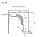
- Examples of the light transmissive device include an arrayed waveguide grating (AWG) including a planar lightwave circuit (PLC) such as shown in Fig. 15.
- the arrayed waveguide grating has a waveguide forming region 10 formed from quartz-based glass on a substrate 1 made of silicon or the like.
- the waveguide forming region 10 has a waveguide structure as illustrated in Fig 15 and formed from a core.
- the waveguide structure of the arrayed waveguide grating includes one or more optical input waveguides 2 arranged side by side, a first slab waveguide 3 connected to the output ends of the optical input waveguides 2, an arrayed waveguide 4 connected to the output end of the first slab waveguide 3, a second slab waveguide 5 connected to the output end of the arrayed waveguide 3, and a plurality of optical output waveguides 6 arranged side by side and connected to the output end of the second slab waveguide 5.
- the arrayed waveguide 4 propagates light output from the first slab waveguide 3, and includes a plurality of channel waveguides 4a arranged side by side. Lengths of adjacent channel waveguides 4a are different from each other with the differences ( ⁇ L) preset.
- the number of optical output waveguides 6 is determined, for example, in accordance with how many light beams having different wavelengths from one another are to be created as a result of demultiplexing or multiplexing of signal light by the arrayed waveguide grating.
- the channel waveguides 4a constituting the arrayed waveguide 4 are usually provided in a large number, for example 100. However, Fig. 15 is simplified and the number of the channel waveguides 4a, the optical output waveguides 6, and the optical input waveguides 2 in Fig. 15 does not reflect the actual number thereof.
- the optical input waveguides 2 are connected to, for example, transmission side optical fibers (not shown), so that light having undergone the wavelength division multiplexing is introduced to the optical input waveguides 2.
- the light output from the optical input waveguides 2 is introduced to the first slab waveguide 3, is diffracted by the diffraction effect thereof and enters the arrayed waveguide 4 to travel along the arrayed waveguide 4.
- the light After traveling through the arrayed waveguide 4, the light reaches the second slab waveguide 5 and then is condensed in the optical output waveguides 6 to be output therefrom. Because of the preset differences in lengths between adjacent channel waveguides 4a of the arrayed waveguides 4, light beams after traveling through the arrayed waveguides 4 havc different phases from one another. The phase front of many light beams from the arrayed waveguide 4 is tilted in accordance with the differences and the position where the light is condensed is determined by the angle of this tilt.
- light beams having different wavelengths are condensed at different positions from one another.
- the optical output waveguides 6 By forming the optical output waveguides 6 at these positions, light beams ⁇ 1 , ⁇ 2 , ... ⁇ n having different wavelengths can be output from the respective optical output waveguides 6 provided for the respective wavelengths.
- the arrayed waveguide grating has an optical multiplexing/demultiplexing function.
- the arrayed waveguide grating can demultiplex light input from the optical input waveguides 2, which has previously undergone the division multiplexing and possesses different wavelengths from one another, into light beams of one or more wavelengths, and then output the light beams from their respective optical output waveguides 6.
- the central wavelength of light to be demultiplexed is in proportion to the differences ( ⁇ L) in lengths of adjacent channel waveguides 4a constituting the arrayed waveguide 4 and to the effective refractive index n e of the channel waveguides 4a.
- the arrayed waveguide grating can be used as a light transmissive device for optical multiplexing/demultiplexing applied to a wavelength division multiplexing transmission system.
- light beams which have undergone wavelength division multiplexing and having wavelengths of ⁇ 1, ⁇ 2, ⁇ 3, .... ⁇ n (n is an integer equal to or larger than 2), respectively, are input to one of the optical input waveguides 2.
- the light beams are diffracted in the first slab waveguides 3, reach the arrayed waveguides 4, and travel through the arrayed waveguides 4 and the second slab waveguides 5.
- the light beams are respectively condensed at different positions determined by their wavelengths, enter different optical output waveguides 6, travel along their respective optical output waveguides 6, and are output from the output ends of the optical output waveguides 6.
- the light beams having different wavelengths can then be further taken out through optical fibers for outputting light (not shown) that are connected to the output ends of the optical output waveguides 6,
- an optical fiber array is prepared for each.
- connection terminal faces of the optical fibers are arranged and fixed into a one-dimensional array.
- the optical fiber array is fixed to the connection terminal faces of the optical output waveguides 6 or to the optical input waveguides 2 to thereby connect the optical fibers to the optical output waveguides 6 or to the optical input waveguides 2.
- the above arrayed waveguide grating has such light transmission characteristics (wavelength characteristics of transmission light intensity in the arrayed waveguide grating) of light beams output from the optical output waveguides 6 such that with the respective light transmission central wavelengths (e.g., ⁇ 1, ⁇ 2, ⁇ 3, opted ⁇ n) as the center, the light transmittance of the output light beams becomes smaller as the wavelength deviates from their respective light transmission central wavelength.
- the respective light transmission central wavelengths e.g., ⁇ 1, ⁇ 2, ⁇ 3, . ⁇ n
- Every light transmission central wavelength ⁇ o is determined by the effective refractive index n e of the arrayed waveguide 4, the difference ( ⁇ L) in length of adjacent channel waveguides 4a of the arrayed waveguide 4, and diffraction order m, and is expressed by the following numerical expression (1).
- ⁇ o n c ⁇ L/m Therefore, the wavelength indicative of the light transmission characteristics with regard to one of the optical output waveguide 6 is not always one, but there may be plural central wavelengths depending on the diffraction order set thereto. It is possible to demultiplex light into a plurality of optical signals having a certain wavelength interval ⁇ (nm) with the light transmission central wavelength ⁇ o as the center. Accordingly, only the central wavelength ⁇ o is considered in the discussion below.
- the arrayed waveguide grating utilizes the principle of reciprocity (reversibility) of an optical circuit and, hence, has the function of an optical multiplexer as well as the function of an optical demultiplexer. That is, in a manner reverse to that already discussed with respect to Fig. 15, a plurality of light beams having different wavelengths from one another may be input to respective optical output waveguides 6.
- the input light beams travel along propagation routes opposite to the routes discussed above with respect to Fig. 15, are multiplexed in the arrayed waveguide 4 and in the first slab waveguide 3, and then are output from one of the optical input waveguides 2,
- the wavelength resolution of the grating is in proportion to the difference in lengths ( ⁇ L) between the channel waveguides 4a of the arrayed waveguides 4, which are one of the components of the grating.
- the arrayed waveguide grating When the arrayed waveguide grating is designed to have a large ⁇ L, it is theoretically possible to multiplex/demultiplex light to accomplish wavelength division multiplexing with a narrow wavelength interval, It is thus theoretically possible for the arrayed waveguide grating to have a function of multiplexing/demultiplexing a plurality of signal light beams, specifically, a function of demultiplexing or multiplexing a plurality of optical signals with a wavelength interval of 1 nm or less, which is a function deemed necessary for optical wavelength division multiplexing communications of high density.
- first flame hydrolysis deposition is used to form an under cladding layer and a core layer on a silicon substrate, then a photomask is prepared on which the waveguide structure of the arrayed waveguide grating is drawn, a transfer is performed by photolithography through the photomask, the arrayed waveguide grating pattern is transferred onto the core layer by reactive ion etching, and then flame hydrolysis deposition is again used to form an over cladding layer, The arrayed waveguide grating is thus manufactured.
- the arrayed waveguide grating of Fig. 15 is conventionally formed with a quartz-based glass material as a main component, and due to temperature dependency of this quartz-based glass material, the light transmission central wavelength ⁇ o of the arrayed waveguide grating shifts depending on the temperature.
- This temperature dependency extends to so great a degree that, for instance, when the change in temperature is 50°C or more in an arrayed wavcguide grating designed and manufactured using setting values generally used in the background art, the light transmission central wavelength shifts by 0.5 nm or more.
- the value 0.5 nm is fatal to an arrayed waveguide grating desired to demultiplex or multiplex light with a very narrow wavelength interval of 1 nm or less.
- the present inventors therefore believe that there is a great importance in realizing an arrayed waveguide grating type optical multiplexer/demultiplexer that can control the temperature dependency of the light transmission central wavelength. According to the view of the present inventors, easiness in manufacturing the arrayed waveguide grating type optical multiplexer/demultiplexer and smallness of insertion loss are also objects significant in putting into practice an arrayed waveguide grating type optical multiplexer/demultiplexer as a device for wavelength division multiplexing communications.
- the present invention has been made in order to address the problems noted above, and an object of the present invention is therefore to provide an arrayed waveguide grating type optical multiplexer/demultiplexer that is easy to manufacture, can reduce temperature dependency of a light transmission central wavelength, and can reduce insertion loss, and to provide a method of manufacturing the same.
- a slab waveguide is divided into two by intersecting planes that intersect the route of the light traveling along the slab waveguide.
- the intersecting planes serve as dividing planes and divide a waveguide forming region into a first waveguide forming region that includes one portion of the divided slab waveguide and a second waveguide forming region that includes the other portion of the divided slab waveguide.
- One or both of the first waveguide forming region and the second waveguide forming region are moved along the dividing planes by a position shifting member. Therefore it is possible to compensate, with the use of the movement by the position shifting member, shifts in light transmission central wavelengths of the arrayed waveguide grating which is caused by, for example, the temperature change of the arrayed waveguide grating.
- the position shifting member when the position shifting member is arranged such that its one end is secured on the first waveguide forming region and its other end is secured on the second waveguide forming region, the structure of the device is simplified and precision is improved, Furthermore, the cost of the device is reduced and the yield thereof is increased.
- At least one slab waveguide is divided into two by intersecting planes that intersect the route of light traveling along the slab waveguide.
- the waveguide forming region is divided by the dividing planes into the first waveguide forming region that includes one portion of the divided slab waveguide and a second waveguide forming region that includes the other portion of the divided slab waveguide.
- a position shifting member with a function of moving one or both of the first and second waveguide forming regions along the dividing planes is fixed before the division such that the position shifting member secures its one end on the first waveguide forming region and secures its other end on the second waveguide forming region. Therefore, the relative positions of the first waveguide forming region and the second waveguide forming region before the division are almost the same as those after the division.
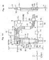
- Figs. 1A and 1B schematically show a first embodiment of an arrayed waveguide grating type optical multiplexer/demultiplexer according to the present invention.
- Fig. 1A is a plan view of the optical multiplexer/demultiplexer of this embodiment.
- Fig, 1B shows a side view of the same viewed from the right in Fig. 1A.
- the first slab waveguide 3 of the arrayed waveguide grating having the structure illustrated in Fig. 15 is divided into two by intersecting dividing planes 8 that intersect with a route of light traveling through the first slab wavcguide 3,
- the intersecting dividing planes 8 are provided in a waveguide forming region 10 starting from one end (upper end in Fig. 1A) of the waveguide forming region 10 and stretching to the midsection thereof.
- Non-intersecting dividing planes 18 that do not intersect with the first slab waveguide 3 are formed so as to connect with the intersecting dividing planes 8.
- the non-intersecting dividing planes 18 may be at right angles with the intersecting dividing planes 8, although that is not a requirement.
- the intersecting dividing planes 8 and the non-intersecting dividing planes 18 divide the waveguide forming region 10 into (1) a first waveguide forming region 10a that includes a divided slab waveguide 3a on one side and (2) a second waveguide forming region 10b that includes a divided slab waveguide 3b on the other side.
- a position shifting member 17 with a thermal expansion coefficient larger than that of the waveguide forming region 10 is provided so as to be secured in the first waveguide forming region 10a at its one end and to be secured in the second waveguide forming region 10b at its other end.
- the position shifting member 17 expands and contracts to slide the first waveguide forming region 10a along the intersecting dividing planes 8 with respect to the second waveguide forming region 10b,
- the position shifting member 17 in this embodiment is placed in a manner that allows the position shifting member 17 to secure its one end on the front side of the waveguide forming region 10a and its other end on the front side of the waveguide forming region 10b.
- This arrangement prohibits the waveguide forming region 10a from being displaced upward (in the direction of the Z axis perpendicular to the X-Y plane) with respect to a base 9, when sliding the waveguide forming region 10a.
- the position shifting member 17 is formed from, for example, a copper plate having a thermal expansion coefficient of 1.65 x 10 -5 (1/K). Beneath the position shifting member 17, solder 30 is provided in each fixing site 29 1 , 29 2 indicated by the oblique broken lines in Fig. 1A. The underside of each solder 30 is coated with a metal film (not shown in Figs. 1A and 1B). One end of the position shifting member 17 is fixed at the fixing site 29 1 to the waveguide region 10a through the metal film and the solder 30, and the other end is fixed at the other fixing site 29 2 to the waveguide forming region 10b in the same manner.
- the first waveguide forming region 10a and the second waveguide forming region 10b are divided and arranged spaced apart.
- the distance between the regions 10a and 10b at an area A in Fig, 1A can be about 100 ⁇ m
- the distance thereof at an area B in Fig. 1A can be about 25 ⁇ m.
- the base 9 is provided below the substrate 1. Holes 15 are formed in attachment portions 9 1 -9 3 that extend outward from the edges of the base 9. Fastening members (such as screws) engaged with the holes 15 are used to fix a chip having the waveguide forming region 10 and the substrate 1 to a housing package 16 (a protective package for the arrayed waveguide grating) shown in Fig. 4,
- the second waveguide forming region 10b may be fixed to the base 9 by clips 19a shown in Fig, 5 as clamping members which clamp the region at two positions.
- a silicon plate 35 as a position shift preventing member may also be provided in a part (shown on the upper side of Fig, 1A) of a border region between the first waveguide forming region 10a and the second waveguide forming region lOb in this embodiment.
- the silicon plate 35 prevents the first waveguide forming region 10a and the second waveguide forming region 10b from shifting their positions in a direction perpendicular to the plane of the substrate 1,
- a plate-like material having a flat surface can be used to form the silicon plate 35.
- the silicon plate 35 can be arranged such that its flat surface abuts with the back side of the substrate 1, and it is clamped by a clip 19b.
- the clip 19b clamps the silicon plate 35 such that the position shifting member 17 can slide the first waveguide forming region 10a along the intersecting dividing planes 8 with respect to the second waveguide forming region 10b.
- the present invention as shown in Figs. 1A and 1B provides an operation such that the position shifting member 17 will expand and contract with changes in temperature. That position shifting is designed in the present invention to shift the two portions of the divided slab waveguide 3a to compensate for temperature induced variations in the arrayed waveguide grating. For the device of the present invention to operate properly then, it is important that the position shifting member 17 expand and contract at an appropriate rate based on the temperature changes.
- the position shifting of the position shifting member 17 is based largely on its material and the length J between the two fixed ends, as it is that unfixed portion of the position shifting member 17 extending along the length J which will expand and contract. As discussed below, a specific example of how to properly calculate that length J is set forth.
- the arrayed waveguide grating type optical multiplexer/demultiplexer according to the first embodiment is an arrayed waveguide grating type optical multiplexer/demultiplexer that is capable of multiplexing and demultiplexing light corresponding to, e.g., sixteen waves with a frequency interval of 100 GHz, and has the following parameters.
- the parameters include FSR (free spectral range) set to 25.6 nm, the diffraction order m set to 59, and the difference ⁇ L in length between adjacent channel waveguides 4a set to 63.1 ⁇ m at a temperature of 25 ° C.
- the parameters also include a focal length L f set to 12327.06 ⁇ m for the first and second slab waveguides 3 and 5, a pitch D of the arrayed waveguide 4 set to 20 ⁇ m, the effective refractive index n c set to 1.45115 for the arrayed waveguide 4, an arrayed waveguide group refractive index n g set to 1.47512, an effective refractive index n s set to 1,453 for the first and second slab waveguides 3 and 5, and the central wavelength ⁇ o of the arrayed waveguide grating set to 1.551 ⁇ m.
- the present inventors have examined (1) the case in which the arrayed waveguide grating type optical multiplexer/demultiplexer is manufactured setting the J to the calculated value J c (17 mm), (2) the case in which the arrayed waveguide grating type optical multiplexer/demultiplexer is manufactured setting the J to the calculated value J c + 5mm (22 mm), and (3) the case in which the arrayed waveguide grating type optical multiplexer/demultiplexer is manufactured setting the J to the calculated value J c - 5mm (12 mm).
- the present inventors found from the data obtained by the above examination and representing the relation between the length J and the temperature dependency of the light transmission central wavelength that the length J should be set to 20 mm in order to make the temperature dependency coefficient of light transmission central wavelength almost 0. Accordingly, the arrayed waveguide grating is manufactured determining the length of the position shifting member 17 and positions to form the solder 30 so that the length J is set to 20. Lengths E and Q shown in Fig, 1A are 60 mm and 5 mm, respectively.
- the metal film mentioned above is formed as follows (see Fig. 2A). First, a resist is applied to the front side of the waveguide forming region 10. The applied resist is exposed using a preset pattern, and is then developed to form a resist mask, Through this resist mask, a metal film 31 is formed by evaporation or sputtering in each fixing site 29 1 , 29 2 on the front side of the waveguide forming region 10. The metal film 31 serves as a base film of the solder 30, and is provided to improve adherence of the solder 30 to the front side (glass surface) of the waveguide forming region 10. This process adopts a general semiconductor manufacturing process which utilizes photolithography and, hence, positioning of high accuracy is not hard to achieve.
- films usable as the metal film 31 include a lamination film including Cr (0.1 ⁇ m) and Cu (0.5 ⁇ m) layered in this order, a lamination film including Cr (0.1 ⁇ m), Ti (0.1 ⁇ m), Pt (0.1 ⁇ m) and Au (0.6 ⁇ m) layered in this order, and a lamination film including Ti (0.1 ⁇ m), Pt (0.1 ⁇ m), and Au (0.6 ⁇ m) layered in this order,
- lift-off is conducted to peel the resist mask off and remove it using a solvent.
- This solvent dissolves only the resist, and acetone, for example, is suitable for the solvent.
- matching oil matching the waveguide forming region 10 in refractive index can be provided in the space between the intersecting dividing planes 8. Furthermore, the matching oil can fill the housing package for housing the arrayed waveguide grating in this embodiment. If the housing package is not filled with the matching oil, matching grease with high viscosity may be provided instead in the space between the intersecting dividing planes 8. Such arrangements make it possible to protect the lightwave circuit module against adverse influence of moisture even in a hot and humid environment. It also prevents evaporation of the refractive index matching agent provided in the space between the intersecting dividing planes 8 of the arrayed waveguide grating. Therefore, it is possible to avoid cracking of the arrayed waveguide grating and to avoid an increase in connection loss at the intersecting dividing planes 8 due to moisture absorption in a hot and humid environment.
- the first embodiment is structured as described above. Now, specific examples are given in relation to a method of manufacturing the arrayed waveguide grating type optical multiplexer/demultiplexer according to the first embodiment.
- an arrayed waveguide grating (arrayed waveguide grating chip) which has the same structure as the background arrayed waveguide grating shown in Fig. 15.
- Dividing line 80 for forming dividing planes that include the intersecting dividing planes 8, 18 (the intersecting dividing planes 8 and the non-intersecting dividing planes 18 in this embodiment) are set in advance.
- the dividing planes are for dividing the waveguide forming region 10 into the first waveguide forming region 10a and the second waveguide forming region 10b.
- the arrayed waveguide grating chip is cut along the line separating the non-intersecting dividing planes 18.
- the metal film 31 is formed in each fixing site 29 1 , 29 2 on the front side of the arrayed waveguide grating chip, A groove is formed on the back side of the arrayed waveguide grating chip along the dividing lines 80, After that, the back side of the arrayed waveguide grating chip is temporarily fixed to a temporal fixing plate 49 made of a flat glass plate at temporal fixing areas 32.
- An adhesive e.g., Cemedine Super 5 (trade name) is applied to each of the temporal fixing areas 32 in a manner of drawing a circle with dots, so that the arrayed waveguide grating chip can later be readily peeled off the temporal fixing plate 49.
- the non-intersecting dividing planes 18 are formed by cutting the arrayed waveguide grating chip by a dicing saw or the like. The width thereof is, for example, about 100 ⁇ m.
- a groove 38 runs along the dividing lines 80 of the intersecting dividing planes 8 and is formed on the back side of the arrayed waveguide grating chip.
- the groove 38 may have a width of about 300 ⁇ m and a depth of about 0.7 mm, for example.
- a groove 37 is formed as shown in Figs, 2B and 2C.
- the groove 37 runs along the dividing lines of the intersecting dividing planes 8 on the front side of the arrayed waveguide grating, and may have a width of about 20 ⁇ m.
- the groove 37 forms, together with the groove 38 formed on the back side of the arrayed waveguide grating, the intersecting dividing planes 8.
- the solder 30, e.g. of Sn/Pb (60%/40%), is then disposed on each area for forming the metal film 31,
- solder 30 is melted while the position shifting member 17 made of copper plate is set in place as shown in Fig. 3A, thereby fixing the position shifting member 17 to the waveguide forming region 10 with the solder 30.
- the solder 30 is provided to adhere the metal film 31 tightly to the position shifting member 17.
- the solder 30 is melted by heating the arrayed waveguide grating up to 230°C using, for example, a hot plate.
- the arrayed waveguide grating chip of the above structure having been temporarily fixed to the temporal fixing plate 49, is immersed in acetone to peel it off the temporal fixing plate 49 as shown in Fig. 3B.
- the waveguide forming region 10 is at this time divided into the first waveguide forming region 10a and the second waveguide forming region lOb by the intersecting dividing planes 8 and the non-intersecting dividing planes 18.
- Optical fiber arrays 21 and 22 next are connected to the arrayed waveguide grating.
- Optical fibers 23 and 24 (Fig, 4) are provided in the optical fiber arrays 21 and 22, respectively.
- the optical fibers 23 and 24 are aligned so that cores thereof are bonded to cores of the optical input waveguides 2 of the arrayed waveguide grating and of the optical output waveguides 6 of the same, respectively.
- the clips 19a fix the waveguide forming region 10b and the substrate 1 underneath thereof to the base 9.
- the silicon plate 35 is arranged so as to abut with the back side of the border region (back side of the substrate 1) between the first waveguide forming region 10a and the second waveguide forming region 10b.
- the clip 19b fixes the silicon plate 35 such that the first waveguide forming region 10a can be slid.
- the silicon plate 35 may be provided on the back side of the waveguide forming region 10 or on the front side of the waveguide forming region 10.
- the arrayed waveguide grating type optical multiplexer/demultiplexer is housed in the housing package 16 as shown in Fig. 4.
- the arrayed waveguide grating is fixed to the housing package 16 using the holes 15 of the base 9. Thereafter, the housing package 16 is filled with the matching oil and is sealed tightly.
- the position shifting member 17 slides the first waveguide forming region 10a along the intersecting dividing planes 8 with changes in the temperature. This sliding compensates for the temperature dependency of the light transmission central wavelengths of the arrayed waveguide grating.
- the position shifting mechanism is composed of the position shifting member 17 being arranged so as to place its one end on the first waveguide forming region 10a and the other end on the second waveguide forming region 10b, simplifying the overall structure of the device. The cost of the device is accordingly reduced and the production yield thereof is improved,
- This first embodiment adopts the above manufacturing method
- the dividing lines 80 for dividing the waveguide forming region 10 into the first waveguide forming region 10a and the second waveguide forming region 10b are set in advance.
- the position shifting member 17 is fixed so as to be secured in the first waveguide forming region 10a at its one end and in the second waveguide forming region 10b at its the other end.
- the waveguide forming region 10 is then divided into the first waveguide forming region lOa and the second waveguide forming region 10b along the dividing lines 80 by peeling it off the temporal fixing plate 49. Therefore, the relative positions of the first waveguide forming region 10a and the second waveguide forming region 10b in the Y direction are the same before and after the division.
- the light transmission characteristics before the division of the arrayed waveguide grating chip thus can be maintained after the division takes place, reducing the insertion loss.
- the present inventors have examined the arrayed waveguide grating type optical multiplexer/demultiplexer of the first embodiment to evaluate whether any increase in insertion loss results when the temperature of the arrayed waveguide grating changes from 5°C to 75°C arises. As a result of that examination, the insertion loss was found to increase by 0.2 dB, which can be deemed as almost no increase.
- the position shifting member 17 is fixed to the front side of the waveguide forming region 10 through the metal film 31 and the solder 30. Therefore, unlike a case in which an adhesive is used to fix the position shifting member 17 to the waveguide forming region 10, the solder 30 will not run outside of the designed pattern but will be contained within, and the position shifting member 17 can be fixed to the waveguide forming region 10 exactly as designed. This makes it possible to manufacture an arrayed waveguide grating high in compensation accuracy of the temperature dependency of the light transmission central wavelengths of the arrayed waveguide grating.
- the clips 19a clamp the second waveguide forming region 10b and the substrate 1 underneath thereof in this first embodiment,
- the second waveguide forming region 10b therefore is hardly influenced by the thermal expansion of the base 9, making it possible to more accurately slide the waveguide forming region 10a with respect to the waveguide forming region 10b. This eliminates the temperature dependency of the light transmission central wavelengths of the arrayed waveguide grating.
- matching oil may be provided in the space between the intersecting dividing planes 8, and the arrayed waveguide grating is housed in the housing package 16 filled with the matching oil. Therefore, as described above, an excellent optical multiplexer/demultiplexer can be manufactured which can avoid an increase in insertion loss even in a hot and humid environment. It is also possible to surely prevent cracking of the arrayed waveguide grating due to moisture absorption from taking place even if it is an arrayed waveguide grating inferior in moisture resistant characteristics.
- Figs. 6A and 6B show the structure of the main part of a second embodiment of an arrayed waveguide grating type optical multiplexer/demultiplexer according to the present invention
- Fig. 6A is a plan view of the optical multiplexer/demultiplexer of this embodiment.
- Fig. 6B is a side view thereof viewed from the right in Fig. 6A, without the optical fibers 24 and the optical fiber array 22,
- the second embodiment is structured in almost the same way as the first embodiment. However, the second embodiment differs from the first embodiment in that it omits the silicon plate 35 in the border region between the first waveguide forming region 10a and the second waveguide forming region 10b of the first embodiment,
- the position shifting member 17 in the second embodiment has a groove 50 formed so as to coincide with the non-intersecting dividing planes 18.
- An example of a method of manufacturing the arrayed waveguide grating type optical multiplexer/demultiplexer according to the second embodiment is shown in Figs. 7A to 8D.
- E 60mm
- F 1mm
- G 2.5mm
- J 20mm
- P 30mm
- Q 5mm
- R 5mm
- S 1mm
- T 25mm
- U 10mm.
- an arrayed waveguide grating chip as shown in Fig. 7A is prepared.
- the dividing lines 80 (not shown) are set in this chip in a manner similar as in the first embodiment, and the metal film 31 (not shown in Fig. 7A) is formed thereon for each end of the position shifting member 17.
- the solder 30 is then formed on each metal film 31 as shown in Fig. 7B.
- the position shifting member 17 is fixed with solder so as to place its one end on the first waveguide forming region 10a and the other end on the second waveguide forming region 10b.
- a plate is selected such that the distance between the waveguide forming region 10a and the waveguide forming region 10b in the intersecting dividing planes 8 (the distance between the intersecting dividing planes 8) is about 25 ⁇ m, and the distance between the waveguide forming region 10a and the waveguide forming region 10b in the non-intersecting dividing planes 18 (the distance between the non-intersecting dividing planes 18) is about 100 ⁇ m.
- the chip is cut along the dividing lines 80 by a dicing saw or the like, thereby forming the intersecting dividing planes 8 and the non-intersecting dividing planes 18 and dividing the waveguide forming region 10 into the first waveguide forming region 10a and the second waveguide forming region 10b.
- a crack may take place starting from the tip of the division in forming the intersecting dividing planes 8 and the non-intersecting dividing planes 18, However, the crack can be avoided completely if, as in the first embodiment, the arrayed waveguide grating is temporarily fixed to the temporal fixing plate 49 while forming the intersecting dividing planes 8 and then the waveguide forming region 10 is divided into the first waveguide forming region 10a and the second waveguide forming region 10b.
- the groove 50 is formed in the position shifting member 17 in the second embodiment. However, the groove 50 is not always required to be formed and it may be omitted. The groove 50 facilitates the work of cutting the waveguide forming region 10 and the substrate 1 using a dicing saw or the like after the position shifting member 17 is fixed with solder.
- the second embodiment is structured as above, and has almost the same effect as in the first embodiment.
- the second embodiment omits the silicon plate 35 that is provided in the first embodiment, it is somewhat less effective in preventing the first and second waveguide forming regions 10a and 10b from shifting their positions in a direction perpendicular to the plane of the substrate I as compared with the first embodiment.
- the second embodiment provides the above preventive effect regarding the position shifting by arranging the position shifting member 17 such that its one end is secured on the first waveguide forming region 10a and its other end is secured on the second waveguide forming region 10b.
- the second embodiment has been found by the inventors to be successful in limiting an increase in insertion loss when the temperature of the arrayed waveguide grating changes from 5°C to 75°C to 0.8 dB.
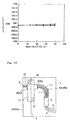
- Fig. 9 shows the results thereof. It is confirmed by Fig. 9 that the arrayed waveguide grating type optical multiplexer/demultiplexers of the second embodiment are optical multiplexers/demultiplexers independent of temperature in which almost no temperature dependency of light transmission wavelengths can be found.
- Fig. 10 shows the structure of the main part of a third embodiment of an arrayed waveguide grating type optical multiplexer/dernultiplexer according to the present invention
- the third embodiment is structured in almost the same way as the first embodiment.
- the third embodiment differs from the first embodiment in that, without forming the non-intersecting dividing planes 18, only the intersecting dividing planes 8 are used to divide the waveguide forming region 10 into the first waveguide forming region 10a and the second waveguide forming region 10b, and in that the position shifting member 17 is provided on the front side of the border region between the first and second waveguide forming regions 10a and 10b.
- the base 9 is provided and the second waveguide forming region 10b is fixed to the base 9 by the clips 19a.
- the dividing lines 80 are set and the metal film 31 is formed for each end of the position shifting member 17.
- a groove 37 having, e.g., a width of about 20 ⁇ m and a depth of about 0,2 mm is formed on the waveguide forming region 10.
- the position shifting member 17 is fixed at its respective ends to each metal film 31 on the front side of the film through solder (not shown).
- the position shifting member 17 is fixed in a manner that allows the position shifting member 17 to set its one end on the first waveguide forming region 10a and its other end on the second waveguide forming region.
- a groove 38 having a width of, e.g., about 300 ⁇ m is then formed on the back side of the arrayed waveguide grating chip to form the intersecting dividing planes 8.
- the third embodiment also can provide the same effects as in the first embodiment, and is successful in limiting an increase in insertion loss when the temperature of the arrayed waveguide grating changes from 5°C to 75°C to 0.2 dB.
- the present invention is not limited to the above embodiments but is capable of adopting various modifications.
- the position shifting member 17 is disclosed as formed from a copper plate in the above discussed embodiments.
- a metal material other than copper may be used to form the position shifting member 17, and a material that is not metal but which has a thermal expansion coefficient larger than that of the waveguide forming region 10 may also be used.
- the metal film 31 may be formed as follows. First, the metal film 31 is formed in a region on the front side of the waveguide forming region 10, the region including areas for forming the solder 30. Then, the resist is applied thereto to conduct exposure and development using the set pattern, namely, photolithography. The metal film 31 is removed by etching (reactive ion etching or wet etching), leaving only the areas for forming the solder 30. The resist is then removed by immersing it in the solvent mentioned above or in oxygen plasma.
- the metal film 31 can be formed precisely in the areas for forming the solder 30 of the preset pattern on the front side of the waveguide forming region 10. After that, a solder chip having almost the same size as the size of the metal film 31 is placed on each metal film 31 in the same manner as in the above discussed embodiments. The position shifting member 17 is thus fixed to the waveguide forming region 10 with solder. The rest of the process follows the manufacturing methods of the foregoing embodiments.
- the arrayed waveguide grating type optical multiplexer/demultiplexer manufactured in this way has the same effect as in the arrayed waveguide grating type optical multiplexer/demultiplexers of the above embodiments.
- the solder 30 used for solder fixing may be fixed to the entire face of the metal film 31. There is no inconvenience if the solder 30 is not completely contained within the regions of metal film 31.
- the material of the solder 30 used for solder fixing of the position shifting member 17 in the arrayed waveguide grating type optical multiplexer/demultiplexer according to the present invention is not limited to the ones mentioned in the preceding embodiments, but is suitably chosen.
- the position shifting member 17 is provided on the front side of the waveguidc forming region 10 in the above discussed embodiments. However, the position shifting member 17 may be provided on the back side of the substrate 1.
- the arrayed waveguide grating is formed utilizing the reciprocity of the optical circuit, Therefore, although it is the first slab waveguide 3 that is divided into two in the above discussed embodiments, the second slab waveguide 5 may be divided instead.
- the second slab waveguide 5 is divided into two, one or both of the divided slab waveguides are slid by the position shifting member 17 along the intersecting dividing planes 8 in a direction that makes the temperature dependency of the light transmission central wavelengths less, This arrangement also provides the same effect as in the above discussed embodiments and eliminates the temperature dependency change of the light transmission central wavelengths.
- the intersecting dividing planes 8 of the first slab waveguide 3 or of the second slab waveguide 5 are not limited to planes almost parallel to the X axis as in the above discussed embodiments.
- the planes may be slanted in the X axis. It is sufficient if the dividing planes intersect with a route of light traveling through the slab waveguide to be divided,
- a plurality of optical input waveguides 2 are provided in the waveguide structure of the arrayed waveguide grating according to the above discussed embodiments.
- the number of optical input waveguides 2 to be provided may be one.
- the waveguide forming region 10b is clamped by the clips 19a to be fixed to the base 9 in the above discussed embodiments, a clamping member other than the clips 19a may be used to fix the waveguide forming region 10b to the base 9. It is also possible to reverse the roles of the waveguide forming regions 10a and 10b by clamping the periphery of the waveguide forming region 10a to fix the region 10a to the base 9, and by then moving the waveguide forming region 10b along the intersecting dividing planes 8.
- the position shifting member 17 in the above discussed embodiments is arranged such that the position shifting member 17 is secured in the first waveguide forming region 10a at its one end and is secured in the second waveguide forming region 10b at its other end.
- the position shifting member 17 can also be arranged as shown in Figs. 12A and 12B and still control the insertion loss of the arrayed waveguide grating type optical multiplexer/demultiplexer.
- the position shifting member 17 is arranged to set its one end on the base 9 and its other end on one or both of the first and second waveguide forming regions 10a and 10b (on the first waveguide forming region 10a in Figs. 12(a), 12(b). This arrangement is obtained by the following manufacturing method.
- An arrayed waveguide grating chip is placed on the base 9 formed from a quartz plate or the like and having a shape of the letter U, as shown in Fig. 13A.
- the dividing line 80 is set in advance. Only the second waveguide forming region 10b is fixed to the base 9 using a thermally curable adhesive or the like. As shown in Figs. 13B and 13C, the position shifting member 17 is then fixed such that the position shifting member 17 secures its one end on the first waveguide forming region 10a and its other end on the base 9.
- the waveguide forming region 10 is thereafter divided into the first waveguide forming region 10a and the second waveguide forming region 10b along the dividing line 80.
- This arrangement maintains the distance between the first waveguide forming region 10a and the second waveguide forming region 10b in the intersecting dividing planes 8. Therefore, the light transmission characteristics before the waveguide forming region 10 is divided can be maintained after the division.
- the arrayed waveguide grating type optical multiplexer/demultiplexer therein may include a position shift preventing member such as the silicon plate 35 shown in Fig. 1A in the border region between the first waveguide forming region 10a and the second waveguide forming region 10b. Precision can be improved in terms of relative positions of the first waveguide forming region 10a and the second waveguide forming region 10b in the Z direction by providing such a position shift preventing member.
- the inventors have found that the insertion loss is increased by about 0.5 dB when the temperature of the arrayed waveguide grating changes from 5°C to 75°C.
- the structure of the base 9 is not particularly limited in the arrayed waveguide grating type optical multiplexer/demultiplexer to which the above manufacturing method is applied.
- the U-shaped base 9 obtained by forming a U groove 40 as above facilitates the division of the arrayed waveguide grating along the dividing lines 80.
- the position shifting member 17 shown in Fig. 12A is more suitable for accurate control of how far the first waveguide forming region 10a is moved.
- the running adhesive 13 in the structure of Fig. 12B may make the length J' in the longitudinal direction of the position shifting member 17, which functions to move the first waveguide forming region 10a, shorter than the length J necessary to accurately move the first waveguide forming region 10a.
- the structure of Fig, 12A can prevent the free running of the adhesive 13 and hence the position shifting member 17 can be fixed more accurately,
- the position shifting member 17 having the structure of Fig. 12A, or to secure the position shifting member 17 through the metal film 31 and the solder 30 on the front side of the waveguide forming region 10 or the back side of the substrate 1 as in the above discussed embodiments,
- Through holes 25 may be formed in the structure where, as shown in Fig, 14A, the intersecting dividing planes 8 that intersect with one or both of the first slab waveguide 3 and the second slab waveguide 5 (the first slab waveguide 3 in Fig. 14A) start from one end of the waveguide forming region 10 and stretch to the midsection thereof, As shown in Figs. 14A and 14B, the through holes 25 (25a and 25b) pierce the waveguide forming region 10 (here, the region 10b) from the front side thereof and reach the substrate 1 to connect with the space between the intersecting dividing planes 8 and the space between the non-intersecting dividing planes 18, respectively.
- the through holes 25a and 25b are formed outside the area where the waveguide structure is formed.
- the side walls of the through holes have smooth surfaces.
- the through hole 25a has a square-like shape in the X-Y plane. Each side of the square may be about 4 mm and each comer thereof may have a radius of curvature of 0.5 mm.
- the through hole 25b may also be circular in the X-Y plane and the diameter thereof may be 2.5 mm,
- the arrayed waveguide grating type optical multiplexer/demultiplexer is reinforced by the through holes 25a and 25b connected with the space between the intersecting dividing planes 8 and the space between the non-intersecting dividing planes 18, respectively, as shown in Figs. 14A and 14B.
- the strength thereof is enhanced against cracking or breakage of the ends of the intersecting dividing planes 8 and of the non-intersecting dividing planes 18 if, e.g., a module packaging the arrayed waveguide grating type optical multiplexer/demultiplexer is dropped by mistake during its handling.
- the through holes 25a and 25b may be respectively formed on the tips of dividing lines after the dividing lines are set.
- the dividing lines are for forming the dividing planes including the intersecting dividing planes 8 (here, the intersecting dividing planes 8 and the non-intersecting dividing planes 18).
- the dividing planes are for dividing the waveguide forming region 10 into the first waveguide forming region 10a and the second waveguide forming region 10b.
- the through holes 25a and 25b may be formed after the dividing lines are set and the metal film 31 is formed,
- the dividing planes such as the intersecting dividing planes 8 and the non-intersecting dividing planes 18 are formed by cutting in the embodiment modes above, However, the cleavage method (split-open) or other methods may be used to form these dividing planes.
- one or both of a first slab waveguide and a second slab waveguide are divided into two by intersecting planes that intersect the route of light traveling along one of the slab waveguides.
- the waveguide forming region is divided by the dividing planes into the first waveguide forming region that includes one divided slab waveguide and a second waveguide forming region that includes the other divided slab waveguide.
- a position shifting member with a function of moving one or both of the first and second waveguide forming regions along the dividing planes is fixed before the division such that the position shifting member secures its one end on the first waveguide forming region and secures its other end on the second waveguide forming region. Therefore, the relative positions of the first waveguide forming region and the second waveguide forming region before the division are almost the same as those after the division.
- the arrayed waveguide grating in a method of manufacturing the arrayed waveguide grating type optical multiplexer/demultiplexer, is placed on a base.
- the waveguide forming region is divided into a first waveguide forming region and a second waveguide forming region.
- a position shifting member with a function of moving one or both of the first and second waveguide forming regions along the dividing planes is fixed before the division such that the member secures its one end on the base and secures its other end on one or both of the first and second waveguide forming regions. Therefore, the relative positions of the first waveguide forming region and the second waveguide forming region before the division are almost the same as those after the division.
- the arrayed waveguide grating type optical multiplexer/demultiplexer manufactured by applying the manufacturing method of the present invention thus can maintain, after the waveguide forming region is divided, the light transmission characteristics before the division,
- first and second slab waveguides are divided into two by intersecting planes that intersect the route of the light traveling along the waveguides.
- the intersecting planes serve as dividing planes and divide the waveguide forming region into a first waveguide forming region that includes one divided slab waveguide and a second waveguide forming region that includes the other divided slab waveguide,
- One or both of the first waveguide forming region and the second waveguide forming region are moved along the dividing planes by a position shifting member. Therefore, it is possible to compensate, with the use of the movement by the position shifting member, shifts in light transmission central wavelengths of the arrayed waveguide grating which is caused by, for example, the temperature change of the arrayed waveguide grating.
- the position shifting member when the position shifting member is arranged such that its one end is secured on the first waveguide forming region and its other end is secured on the second waveguide forming region, the structure of the device is simplified and precision is improved. Furthermore, the cost of the device is reduced and the yield thereof is increased.
- the position shifting member is fixed to the waveguide forming region through the solder and the metal films.
- the position shifting member thus can be fixed exactly as designed without fear of adhesive running uncontrollably. This makes an excellent arrayed waveguide grating that has high temperature compensation precision of light transmission wavelengths of the arrayed waveguide grating.
- one of the first waveguide forming region and the second waveguide forming region is fixed, whereas the other is moved by the position shifting member.
- the fixed waveguide forming region is clamped by the clamping member and held to the base of the arrayed waveguide grating type optical multiplexer/demultiplexer. Fixing one waveguide region makes it easy to smoothly move the other waveguide forming region.
- one of the first waveguide forming region and the second waveguide forming region is fixed, whereas the other is moved by the position shifting member.
- a position shift preventing member for preventing the first and second waveguide forming regions from shifting toward the direction perpendicular to the substrate plane is provided in at least a part of the border region between the first waveguide forming region and the second waveguide forming region. The first and second waveguide forming regions are thus prevented from shifting toward the direction perpendicular to the substrate plane. Therefore, an increase in insertion loss by this positional shift can be controlled.
- the position shift preventing member is formed from a plate-like material having a flat surface, and is arranged such that the flat surface abuts with the front side of the waveguide forming region or the back side of the substrate,
- the shift position preventing member can readily be formed using the plate-like material, and the positional shift of the first and second waveguide forming regions toward the direction perpendicular to the substrate plane can be prevented.
- the position shifting member is a metal member
- a metal member having a large thermal expansion rate is used to form the position shifting member.
- the arrayed waveguide grating type optical multiplexer/demultiplexer of the present invention is thus readily manufactured.
- through holes piercing the waveguide forming region and reaching the substrate are formed from the front side of the waveguide forming region in areas outside the waveguide structure.
- the side walls of the through holes have smooth surfaces.
- the dividing planes that intersect with one or both of the first slab waveguide and the second slab waveguide start from one end of the waveguide forming region and stretch to the midsection thereof to communicate with the through holes. This enhances the strength thereof against cracking or breakage of the ends of the dividing planes when, e.g., a module packaging the arrayed waveguide grating type optical multiplexer/demultiplexer is dropped by mistake during its handling.
- the position shifting member 17 has an operation to expand and contract to move one or both of the first and second waveguide forming regions along the dividing planes.
- the position shifting member 17 operates as an expansion/contraction member,
- other mechanisms for moving one or both of the first and second waveguides relative to each other could also be implemented instead of relying on a device which expands and contracts, as in the embodiments noted above.
- a stepping motor could be utilized to shift one or both of the first and second waveguides relative to each other based on a sensed temperature.
- One of the important features of the present invention is that one or both of the first and second waveguides is shifted relative to each other, and other mechanisms which can induce such a shifting are also possible within the scope of the present invention.
Landscapes
- Physics & Mathematics (AREA)
- Engineering & Computer Science (AREA)
- Microelectronics & Electronic Packaging (AREA)
- General Physics & Mathematics (AREA)
- Optics & Photonics (AREA)
- Optical Integrated Circuits (AREA)
Abstract
Description
Claims (22)
- A method of manufacturing an arrayed waveguide grating optical multiplexer/demultiplexer, comprising the steps of:preparing an arrayed waveguide grating having a waveguide forming region for forming a waveguide structure and at least one slab waveguide;setting dividing lines for determining dividing planes that intersect a route of light traveling along said at least one slab waveguide, said dividing planes dividing said at least one slab waveguide into first and second divided slab waveguide portions, and also dividing said waveguide forming region into a first waveguide forming region that includes the first divided slab waveguide portion and a second waveguide forming region that includes the second divided slab waveguide;fixing a position shifting member to have a first end secured on said first waveguide forming region and to have a second end secured on said second waveguide forming region; anddividing said waveguide forming region into said first waveguide forming region and said second waveguide forming region along said dividing lines.
- A method of manufacturing an arrayed waveguide grating optical multiplexer/demultiplexer according to claim 1, further comprising the step of:
placing said arrayed waveguide grating on a base prior to said step of setting dividing lines, - A method of manufacturing an arrayed waveguide grating optical multiplexer/demultiplexer according to claim 1, wherein said at least one slab waveguide includes first and second slab waveguides, and said prepared arrayed waveguide grating further includes:one or more optical input waveguides arranged side by side;said first slab waveguide connected to output ends of said optical input waveguides;an arrayed waveguide connected to an output end of said first slab waveguide and including a plurality of channel waveguides arranged side by side, for transmitting light that has traveled through said first slab waveguide, said channel waveguides having different predetermined lengths;said second slab waveguide connected to an output end of said arrayed waveguide; andone or more optical output waveguides arranged side by side and connected to an output end of said second slab waveguide.
- A method of manufacturing an arrayed waveguide grating optical multiplexer/demultiplexer according to claim 3, further comprising the step of:
placing said arrayed waveguide grating on a base prior to said step of setting said dividing lines. - An arrayed waveguide grating optical multiplexer/demultiplexer, comprising:a waveguide forming region configured to form a waveguide structure and including at least one slab waveguide, wherein said at least one slab waveguide is divided into two by dividing planes that intersect a route of light traveling along said at least one slab waveguide to form first and second divided slab waveguide portions, and wherein said waveguide forming region is divided by the dividing planes that divide said at least one slab waveguide, into a first waveguide forming region that includes the first divided slab waveguide and a second waveguide forming region that includes the second divided slab waveguide; anda position shifting member having a first end secured to said first waveguide forming region and a second end secured to said second waveguide forming region, said position shifting member configured to move at least one of said first waveguide forming region and said second waveguide forming region along said dividing planes.
- An arrayed waveguide grating optical multiplexer/demultiplexer according to claim 5, wherein said position shifting member expands and contracts.
- , An arrayed waveguide grating optical multiplexer/demultiplexer according to claim 5, further comprising:
a base on which said arrayed waveguide grating is placed. - An arrayed waveguide grating optical multiplexer/demultiplexer according to claim 5, wherein said at least one slab waveguide includes first and second slab waveguides, and further comprising:one or more optical input waveguides arranged side by side;said first slab waveguide connected to output ends of said optical input waveguides;an arrayed waveguide connected to an output end of said first slab waveguide and including a plurality of channel waveguides arranged side by side, and configured to transmit light that has traveled through said first slab waveguide, said channel waveguides having different predetermined lengths;said second slab waveguide connected to an output end of said arrayed waveguide; andone or more optical output waveguides arranged side by side and connected to an output end of said second slab waveguide.
- An arrayed waveguide grating optical multiplexer/demultiplexer according to claim 5, farther comprising:metal films formed in said waveguide forming region;solder provided on said metal films; andwherein said position shifting member is fixed to said waveguide forming region through said solder and said metal films.
- An arrayed waveguide grating type optical multiplexer/demultiplexer according to claim 7, wherein one of said first waveguide forming region and said second waveguide forming region is fixed whereas the other is moved by said position shifting member, and further comprising:
a clamping member configured to clamp the fixed waveguide forming region to said base. - An arrayed waveguide grating type optical multiplexer/demultiplexer according to claim 5, wherein one of said first waveguide forming region and said second waveguide forming region is fixed whereas the other is moved by said position shifting member, and further comprising:
a position shift preventing member configured to prevent said first and second waveguide forming regions from shifting in a direction perpendicular to a substrate plane, said position shift preventing member provided in at least a part of a border region between said first waveguide forming region and said second waveguide forming region. - An arrayed waveguide grating type optical multiplexer/demultiplexer according to claim 11, wherein said position shift preventing member is formed from a plate-like material having a flat surface and is arranged such that the flat surface abuts with a front side of said waveguide forming region or a back side of said substrate.
- , An arrayed waveguide grating type optical multiplexer/demultiplexer according to claim 6, wherein said position shifting member is a metal member.
- An arrayed waveguide grating type optical multiplexer/demultiplexer according to claim 5, further comprising;through holes piercing said waveguide forming region and reaching a substrate and formed in said waveguide forming region in areas outside said waveguide structure;wherein side walls of said through holes have smooth surfaces; andwherein said dividing planes that intersect said at least one slab waveguide start from one end of said waveguide forming region and extend to connect with said through holes.
- An arrayed waveguide grating optical multiplexer/demultiplexer, comprising:waveguide forming means for forming a waveguide structure and including at least one slab waveguide means, wherein said at least one slab waveguide means is divided into two by dividing means for intersecting a route of light traveling along said at least one slab waveguide means to form first and second divided slab waveguide means, and wherein said waveguide forming means is divided by the dividing means that divide said at least one slab waveguide means into a first waveguide forming region means that includes the first divided slab waveguide means and a second waveguide forming region means that includes the second divided slab waveguide means; andposition shifting means for moving at least one of said first waveguide forming region means and said second waveguide forming region means along said dividing means.
- , An arrayed waveguide grating optical multiplexer/demultiplexer according to claim 15, wherein said position shifting means expands and contracts.
- An arrayed waveguide grating optical multiplexer/demultiplexer according to claim 15, further comprising:
base means for placing said arrayed waveguide grating thereon. - An array waveguide optical multiplexer/demultiplexer according to claim 15, wherein said at least one slab waveguide means includes first and second slab waveguide means, and further comprising:optical input waveguide means;said first slab waveguide connected to an output end of said optical input waveguide means;arrayed waveguide means connected to an output end of said first slab waveguide means for transmitting light that has traveled through said first slab waveguide;said second slab waveguide means connected to an output end of said arrayed waveguide means; andoptical output waveguide means connected to an output end of said second slab waveguide means.
- An arrayed waveguide grating optical multiplexer/demultiplexer according to claim 15, further comprising:metal film means formed in said waveguide forming means;solder means provided on said metal film means; andwherein said position shifting means is fixed to said waveguide forming means through said solder means and said metal film means.
- An arrayed wavcguide grating type optical multiplexer/demultiplexer according to claim 19, further comprising:
clamping means for clamping one of said first and second waveguide forming region means to said base means. - , An arrayed waveguide grating type optical multiplexer/demultiplexer according to claim 19, further comprising:
position shift preventing means for preventing said first and second waveguide forming region means from shifting in a direction perpendicular to a substrate plane. - , An arrayed waveguide grating type optical multiplexer/demulfiplexer according to claim 19, further comprising:through hole means for piercing said waveguide forming region and reaching a substrate; andwherein said dividing means that intersect said at least one slab waveguide means start from one end of said waveguide forming region means and extend to connect with said through hole means.
Applications Claiming Priority (6)
| Application Number | Priority Date | Filing Date | Title |
|---|---|---|---|
| JP37045799 | 1999-12-27 | ||
| JP37045799 | 1999-12-27 | ||
| JP2000176691 | 2000-06-13 | ||
| JP2000176691 | 2000-06-13 | ||
| JP2000283806A JP2002071994A (en) | 1999-12-27 | 2000-09-19 | Array waveguide diffraction grating type optical multiplexer / demultiplexer and method of manufacturing the same |
| JP2000283806 | 2000-09-19 |
Publications (2)
| Publication Number | Publication Date |
|---|---|
| EP1113298A2 true EP1113298A2 (en) | 2001-07-04 |
| EP1113298A3 EP1113298A3 (en) | 2004-02-25 |
Family
ID=27341803
Family Applications (1)
| Application Number | Title | Priority Date | Filing Date |
|---|---|---|---|
| EP00311704A Withdrawn EP1113298A3 (en) | 1999-12-27 | 2000-12-27 | Arrayed waveguide grating multiplexer with temperature compensation |
Country Status (5)
| Country | Link |
|---|---|
| US (1) | US6456763B2 (en) |
| EP (1) | EP1113298A3 (en) |
| JP (1) | JP2002071994A (en) |
| KR (1) | KR100360766B1 (en) |
| CN (1) | CN1178421C (en) |
Cited By (3)
| Publication number | Priority date | Publication date | Assignee | Title |
|---|---|---|---|---|
| DE10210534A1 (en) * | 2002-03-05 | 2003-10-02 | Infineon Technologies Ag | Arrayed waveguide grating optical multiplexer/demultiplexer for optical communication uses split free radiation zone moved by beam for temperature compensation |
| EP1260837A4 (en) * | 2000-10-13 | 2005-11-09 | Furukawa Electric Co Ltd | Array waveguide type diffraction grating and light transmitting center wavelength correcting method |
| CN108803711A (en) * | 2018-05-07 | 2018-11-13 | 河南仕佳光子科技股份有限公司 | A kind of wide warm high stability temperature self-adaptation flattening compensation device |
Families Citing this family (26)
| Publication number | Priority date | Publication date | Assignee | Title |
|---|---|---|---|---|
| JP4460031B2 (en) * | 2000-03-28 | 2010-05-12 | 古河電気工業株式会社 | Arrayed waveguide grating |
| JP3630085B2 (en) * | 2000-09-14 | 2005-03-16 | 日本電気株式会社 | Method for manufacturing arrayed waveguide grating element and arrayed waveguide grating element |
| JP4143257B2 (en) * | 2000-12-06 | 2008-09-03 | 日本電気株式会社 | Arrayed waveguide grating and arrayed waveguide grating module |
| JP3764105B2 (en) * | 2001-03-13 | 2006-04-05 | 古河電気工業株式会社 | Arrayed waveguide grating optical multiplexer / demultiplexer |
| US6735364B2 (en) * | 2001-08-27 | 2004-05-11 | The Furukawa Electric Co., Ltd. | Arrayed waveguide grating optical multiplexer/demultiplexer and method for manufacturing the same |
| US6603892B1 (en) * | 2001-10-24 | 2003-08-05 | Lightwave Microsystems Corporation | Mechanical beam steering for optical integrated circuits |
| US6738545B1 (en) * | 2002-03-18 | 2004-05-18 | Lightwave Microsystems Corporation | Athermal AWG and AWG with low power consumption using groove of changeable width |
| US6954566B2 (en) * | 2002-07-25 | 2005-10-11 | Intel Corporation | Apparatus for thermal compensation of an arrayed waveguide grating |
| US20040037531A1 (en) * | 2002-08-20 | 2004-02-26 | Andrews Mark P. | Waveguide device with a tailored thermal response |
| JP4028340B2 (en) * | 2002-10-01 | 2007-12-26 | 古河電気工業株式会社 | Temperature compensated optical fiber grating components |
| JP4688869B2 (en) * | 2004-05-05 | 2011-05-25 | ネオフォトニクス・コーポレイション | Low power AWG using athermal AWG and variable width grooves |
| JP2007065562A (en) * | 2005-09-02 | 2007-03-15 | Furukawa Electric Co Ltd:The | Arrayed waveguide grating |
| KR100841223B1 (en) * | 2006-02-28 | 2008-06-26 | (주)포인테크 | Temperature-Independent Optical Waveguide Grating Circuit Device for Compensation of Optical Characteristics and Fabrication Method thereof |
| JP5100175B2 (en) * | 2007-03-28 | 2012-12-19 | 古河電気工業株式会社 | Arrayed waveguide grating type multiplexer / demultiplexer |
| JP2010152177A (en) * | 2008-12-25 | 2010-07-08 | Furukawa Electric Co Ltd:The | Athermal awg module |
| US8494319B2 (en) * | 2009-02-26 | 2013-07-23 | Aidi Corporation | Arrayed waveguide grating (AWG) with different radii in the input and output slab regions |
| CN101840030B (en) * | 2009-12-25 | 2012-03-21 | 武汉光迅科技股份有限公司 | Heatless AWG preparation method based on curved array waveguide grating |
| CN102959440A (en) * | 2010-07-02 | 2013-03-06 | 古河电气工业株式会社 | Arrayed waveguide grating optical division multiplexing module |
| CN102193149A (en) * | 2011-06-03 | 2011-09-21 | 珠海保税区光联通讯技术有限公司 | Afebrile array waveguide grating wavelength division multiplexer |
| US8538212B2 (en) | 2011-06-03 | 2013-09-17 | Neophotonics Corporation | Thermally compensated arrayed waveguide grating assemblies |
| US9110232B2 (en) | 2011-06-03 | 2015-08-18 | Neophotonics Corporation | Thermally compensated arrayed waveguide grating assemblies |
| US8565600B2 (en) | 2011-06-10 | 2013-10-22 | Neophotonics Corporation | Optical network configurations with multiple band multiplexing and de-multiplexing and AWG structures with multiple band processing |
| CN104503026B (en) * | 2014-12-12 | 2017-07-04 | 武汉光迅科技股份有限公司 | A kind of afebrile array waveguide grating wavelength division multiplexer and its manufacture method |
| WO2017015578A1 (en) | 2015-07-22 | 2017-01-26 | Miroslaw Florjanczyk | Compound semiconductor photonic integrated circuit with dielectric waveguide |
| KR101885498B1 (en) * | 2018-01-24 | 2018-08-03 | 주식회사 폴스랩 | Athermal arrayed waveguide grating using precision parallel movement module and manufacturing method thereof |
| US20250264660A1 (en) * | 2024-02-21 | 2025-08-21 | Applied Materials, Inc. | Offloading photonic integrated circuit functionality into optical interconnects |
Family Cites Families (7)
| Publication number | Priority date | Publication date | Assignee | Title |
|---|---|---|---|---|
| US5617234A (en) * | 1994-09-26 | 1997-04-01 | Nippon Telegraph & Telephone Corporation | Multiwavelength simultaneous monitoring circuit employing arrayed-waveguide grating |
| TW355752B (en) * | 1996-09-27 | 1999-04-11 | Siemens Ag | Optical coupling-device to couple the light between two waveguide-end-face |
| US6304687B1 (en) * | 1997-02-14 | 2001-10-16 | Nippon Telegraph And Telephone Corporation | Optical waveguide circuit, its manufacturing method and optical waveguide module having the optical waveguide circuit |
| FR2770307B1 (en) * | 1997-10-27 | 1999-11-26 | Commissariat Energie Atomique | PHASE ARRAY OR PHASAR DEVICE AND MANUFACTURING METHOD THEREOF |
| US5905824A (en) * | 1997-12-09 | 1999-05-18 | Delisle; Vincent | Temperature compensated insensitive optical multiplexor/demultiplexor |
| JP2000292632A (en) | 1999-04-01 | 2000-10-20 | Nippon Telegr & Teleph Corp <Ntt> | Temperature independent waveguide |
| JP3434489B2 (en) * | 1999-09-24 | 2003-08-11 | 古河電気工業株式会社 | Array waveguide type diffraction grating |
-
2000
- 2000-09-19 JP JP2000283806A patent/JP2002071994A/en active Pending
- 2000-12-22 US US09/741,792 patent/US6456763B2/en not_active Expired - Fee Related
- 2000-12-27 KR KR1020000083060A patent/KR100360766B1/en not_active Expired - Fee Related
- 2000-12-27 EP EP00311704A patent/EP1113298A3/en not_active Withdrawn
- 2000-12-27 CN CNB001377779A patent/CN1178421C/en not_active Expired - Fee Related
Cited By (4)
| Publication number | Priority date | Publication date | Assignee | Title |
|---|---|---|---|---|
| EP1260837A4 (en) * | 2000-10-13 | 2005-11-09 | Furukawa Electric Co Ltd | Array waveguide type diffraction grating and light transmitting center wavelength correcting method |
| DE10210534A1 (en) * | 2002-03-05 | 2003-10-02 | Infineon Technologies Ag | Arrayed waveguide grating optical multiplexer/demultiplexer for optical communication uses split free radiation zone moved by beam for temperature compensation |
| DE10210534B4 (en) * | 2002-03-05 | 2004-02-05 | Infineon Technologies Ag | Device for multiplexing and / or demultiplexing optical data channels of different wavelengths and method for their production |
| CN108803711A (en) * | 2018-05-07 | 2018-11-13 | 河南仕佳光子科技股份有限公司 | A kind of wide warm high stability temperature self-adaptation flattening compensation device |
Also Published As
| Publication number | Publication date |
|---|---|
| US20010006570A1 (en) | 2001-07-05 |
| US6456763B2 (en) | 2002-09-24 |
| KR20010062781A (en) | 2001-07-07 |
| KR100360766B1 (en) | 2002-11-21 |
| CN1178421C (en) | 2004-12-01 |
| EP1113298A3 (en) | 2004-02-25 |
| CN1302131A (en) | 2001-07-04 |
| JP2002071994A (en) | 2002-03-12 |
Similar Documents
| Publication | Publication Date | Title |
|---|---|---|
| US6456763B2 (en) | Arrayed waveguide grating type optical multiplexer/demultiplexer and a method of manufacturing the same | |
| US6222963B1 (en) | Phased array device or phasar and process for manufacturing this device | |
| JP3434489B2 (en) | Array waveguide type diffraction grating | |
| US6563986B2 (en) | Arrayed waveguide grating | |
| EP1743201B1 (en) | Athermal awg and awg with low power consumption using groove of changeable width | |
| JP2012014071A (en) | Array waveguide diffraction grating type optical multiplexer/demultiplexer | |
| EP1291683A1 (en) | Array waveguide diffraction grating | |
| JP4494599B2 (en) | Arrayed waveguide grating optical multiplexer / demultiplexer | |
| US7965912B2 (en) | Temperature insensitive arrayed waveguide grating multiplexer for optical property compensation and the manufacturing method thereof | |
| US7555176B2 (en) | Method for producing an optical splitter, and optical splitter | |
| US6735364B2 (en) | Arrayed waveguide grating optical multiplexer/demultiplexer and method for manufacturing the same | |
| US6668117B2 (en) | Arrayed waveguide grating optical multiplexer demultiplexer | |
| JP4667927B2 (en) | Arrayed waveguide grating optical multiplexer / demultiplexer | |
| JPWO2012002368A1 (en) | Arrayed waveguide grating optical multiplexer / demultiplexer | |
| JP5075048B2 (en) | Alignment method for arrayed waveguide grating and alignment device for arrayed waveguide grating | |
| US20030031412A1 (en) | Optical arrayed waveguide grating devices | |
| JP2003066254A (en) | Array waveguide diffraction grating type optical multiplexer / demultiplexer and method of manufacturing the same | |
| EP1376171A1 (en) | Optical device for reducing temperature related shift | |
| JP2004020737A (en) | Array waveguide diffraction grating and method of manufacturing the same | |
| JP4316088B2 (en) | Arrayed waveguide grating | |
| JP2001154043A (en) | Optical wavelength multiplexer / demultiplexer and manufacturing method thereof | |
| JP2001330739A (en) | Array waveguide type diffraction grating | |
| JP2002122749A (en) | Optical wavelength multiplexer / demultiplexer | |
| JP2010097231A (en) | Array waveguide diffraction grating type optical multiplexer/demultiplexer | |
| JP2004045696A (en) | Optical waveguide circuit and optical waveguide circuit module |
Legal Events
| Date | Code | Title | Description |
|---|---|---|---|
| PUAI | Public reference made under article 153(3) epc to a published international application that has entered the european phase |
Free format text: ORIGINAL CODE: 0009012 |
|
| 17P | Request for examination filed |
Effective date: 20010112 |
|
| AK | Designated contracting states |
Kind code of ref document: A2 Designated state(s): AT BE CH CY DE DK ES FI FR GB GR IE IT LI LU MC NL PT SE TR |
|
| AX | Request for extension of the european patent |
Free format text: AL;LT;LV;MK;RO;SI |
|
| PUAL | Search report despatched |
Free format text: ORIGINAL CODE: 0009013 |
|
| AK | Designated contracting states |
Kind code of ref document: A3 Designated state(s): AT BE CH CY DE DK ES FI FR GB GR IE IT LI LU MC NL PT SE TR |
|
| AX | Request for extension of the european patent |
Extension state: AL LT LV MK RO SI |
|
| RIC1 | Information provided on ipc code assigned before grant |
Ipc: 7G 02B 6/34 B Ipc: 7G 02B 6/293 A |
|
| 17Q | First examination report despatched |
Effective date: 20040928 |
|
| AKX | Designation fees paid |
Designated state(s): DE FR GB |
|
| STAA | Information on the status of an ep patent application or granted ep patent |
Free format text: STATUS: THE APPLICATION IS DEEMED TO BE WITHDRAWN |
|
| 18D | Application deemed to be withdrawn |
Effective date: 20050409 |