TECHNICAL FIELD
-
The present invention relates to program modification, and more
specifically, to program modification used in a computer system which
executes programs fixed on instruction ROM and the like.
BACKGROUND ART
(General Background)
-
Conventional program modification devices include devices with a
register for modification and devices containing indirect jump instructions
in programs.
-
One such program modification device will be described as follows
with reference to the drawings. (This device should be more strictly
referred to as a program device provided with a function of modifying and
executing programs fixed on ROM or the like; however, it is simply referred
to as the program modification device).
-
Figure 1 shows the entire structure of this conventional program
modification device, and Figure 2 shows the details of its main part.
-
In Figure 1 the program modification device comprises a CPU core
unit 1 including an execution unit 2 and an instruction acquisition unit 3,
an instruction ROM 4 which stores programs, a program monitor unit 5
which checks whether the program portion which is going to be executed is
a program portion (program data) to be modified or not, and an acquired
instruction switch unit 6 which switches between acquiring the instruction
the instruction acquisition unit 3 is going to execute from the instruction
ROM 4 or acquiring it from a modification target program storage memory
A, which will be described later, based on the determination of the program
monitor unit 4.
-
The program modification device further comprises modifying address
registers 7 which store the addresses of program data that need to be
modified (hereinafter referred to as the modification source program data)
and the addresses of program data that are modified and executed instead
of the modification source program data (hereinafter referred to as the
modification target program data) in pairs; a modification target program
storage memory A 8 which stores modification target program data; an
indirect call instruction row 9 contained in the instruction ROM 4; an
indirect call table 10 which is referred to by the indirect call instruction
row 9; and a modification target program storage memory B 11 which
stores branch target program data branching in the indirect call table 10
(when there is no modification in a program, the branch target in the
indirect call table 10 is in the ROM 4).
-
It goes without saying that this program modification device may
further comprise a CRT or a liquid crystal display device, a keyboard, clock
signal generation means, CD-ROM readout means, and a code correction
unit, depending on the use of the computer system equipped with the
program modification device.
-
In terms of the object of the present invention, the modification target
program storage memory A 8 and the modifying address registers 7 are
dispensable unless the programs in the instruction ROM 4 or the CD-ROM
have errors.
-
The three technical terms uniquely used in the present specification
will be defined as follows.
-
The term "program" indicates, when used alone, the entire program
about a specific object executed by the CPU in a DVD drive or the like and
the entire data attached to the program if any, and indicates, when used in
a component of the present invention like "modification target program
storage memory" or "modification source program address", it includes the
concept of "program data" which will be described later. In some cases,
the term indicates not only programs for a CPU system, but also display
instruction programs for digital information such as images or music, or
digitized data such as books or dictionaries and their displays.
-
The term "program data" indicates, of the above-mentioned programs
and the data attached to them, the portion of an error correction target or
the portion attached to this. Thus, not only a part of the program itself,
but also a part of the data used to execute the program is included. To be
more specific, in programs whose execution may branch or change in
accordance with the direction or selection of the user, such as TV games,
various guides and introductions or educational programs, the term
includes the data used only for the branches or changes. The term further
includes a part of the correct program stored integrally with the wrong
program data with regard to the addresses.
-
The term "address" indicates information to specify the storage
positions in a series of modification target program data and modification
source program data. The term includes not only addresses themselves,
but also a so-called address group consisting of consecutive addresses, a
specific region on memory, and a specific one memory among plural
memories.
-
The following is a continuation of the description of the conventional
program modification device.
-
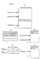
Figure 2 (1) is a conceptual illustration showing the inside of the
instruction ROM 4. Figure 2 (2) is a conceptual illustration showing the
inside of the modifying address registers 7. Figure 2 (3) is a conceptual
illustration showing the inside of the modification target program storage
memory A 8. Figure 2 (4) is a conceptual illustration showing the inside of
the indirect call table 10. Figure 2 (5) is a conceptual illustration of the
modification target program storage memory B 11.
-
The behavior of the program modification device will be described as
follows.
-
Assume that addresses A1 and A2 in the instruction ROM 4 shown in
Figure 2 (1) are the addresses of the modification source program data with
errors, and the program data at addresses B1 and B2 shown in Figure 2 (2)
are executed instead of the program data at these addresses A1 and A2,
respectively.
-
Also assume that the indirect call instruction row in the
instruction
ROM 4 shown in Figure 2 (1), which branches to the address a1 in the
instruction ROM 4, is so modified as to branch to the address b1 in the
modification target
program memory B 11 as shown in Figure 2 (4).
- 1) In order to execute the program data of the addresses B1 and B2
instead of the program data of the addresses A1 and A2, the addresses A1
and B1 as a pair and the addresses A2 and B2 as another pair are written
into the modifying address registers 7 as shown in Figure 2 (2).
Furthermore, the indirect call table 10 shown in Figure 2 (4) is changed
from the address a1 which is before the modification to the address b1
which is after the modification.
- 2) The instruction acquisition unit 3 sequentially acquires
instructions from the instruction ROM 4, and the execution unit 2 executes
the instructions.
- 3) The program monitor unit 5 continuously checks whether or not
the address of program data acquired by the instruction acquisition unit 3
agrees with the address of the modification source program data in the
modifying address registers 7 by referring to the modifying address
registers 7.
- 4) When the instruction acquisition unit 3 tries to acquire program
data from the address A1 in the instruction ROM 4, the program monitor
unit 5 detects agreement between the address 1 and the address of the
modification source program data which is written in the modifying
address registers 7. Then, the program monitor unit 5 makes the acquired
instruction switch unit 6 acquire not the program data at the address A1
but the program data at the address B1, which is stored with the address
A1 in a pair.
- 5) The acquired instruction switch unit 6 switches the instruction
acquisition unit 3 so that the unit 3 acquires instructions not from the
address A1 in the instruction ROM 4 but from the address B1 on the
modification target program storage memory A 8. As a result, the
program data at the address A1 in the instruction ROM 4 are modified into
the program data at the address B1 on the modification target program
storage memory A 8. In the same procedure, the program data at the
address A2 is modified into the program data at the address B2.
- 6) The instruction acquisition unit 3 acquires instructions from the
indirect call instruction row on the instruction ROM 4, and the execution
unit 2 executes the instructions. If it is before the modification of the
program (before the change of the indirect call table 10), the indirect call
table 10 is referred to so as to acquire instructions from the address a1.
-
-
In reality, the indirect call table 10 is changed from the address al to
the address b1, so that after the execution of the indirect call instruction,
instructions are acquired from the address b1. This indicates that the
program data at the address a1 in the instruction ROM 4 have been
modified into the program data on the modification target program storage
memory B 11.
-
In the above-mentioned procedure, inherently non-modifiable errors
in the programs fixed on the instruction ROM or the like or found after the
fabrication of ROM can be modified.
-
Of the modification target program storage memories A 8 and B 11
shown in Figure 1, either one could be used, or they could be physically
one.
-
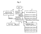
As another conventional device, Figure 3 shows another system which
is basically the same the above-mentioned conventional device. In Figure
3 a built-in ROM 41 corresponds to the instruction ROM 4 shown in Figure
1, and a PC 1 and a decoder 2 correspond to the CPU core unit 1 shown in
Figure 1. The acquired instruction switch unit 6 is a kind of selector.
When the program monitor unit 5 receives the address of a modification
source program, the acquired instruction switch unit 6 receives the
corresponding modification target program data from a modification target
program memory 81 at the same time, and forwards the program data to
the decoder 2.
-
These techniques will not be described any further because these are
disclosed in Japanese Laid-Open Patent Applications No.7-73032,
No.3-186927, No. 3-33926, U.S. Patent No. 5592613, and the like.
(Background Art in terms of the Problems the Invention is going to solve)
-
In the aforementioned structure, however, in order to modify a
program at plural positions, a pair of modifying address registers are
needed for each position. Therefore, as shown in Figure 2 (2), a large
number of registers are required as modifying address registers, which
leads to an increases in hardware scale. (In storing the same amount of
information, an increase in hardware scale is tremendous because registers
demand about 50 times as large as circuit size as memories).
-
When program modification is performed by an indirect call, it is
possible only from the position where the indirect call instruction row is
arranged. Therefore, even when there are only a few steps in a program
which are desired to be modified, it is necessary to store (or write), as a
modified program, the steps from the indirect call instruction row portion
to the modified portion which do not actually need to be modified. This
unnecessarily increases the modification target program in size in the
modification target program storage memories A 8 and B 11.
-
When the program modification device is incorporated into a system,
programs are usually put in the form of ROM chips. When bugs are found
in a ROMed program, the ROM must be modified; however, it takes about
5 weeks to complete modified ROM chips. This may cause to miss the
timing of the introduction of a set device with the ROM chips on the
market. Avoiding this program requires a ROM program modification
function. However, the addition of the function leads to an increase in the
number of registers (modifying address registers) which are highly unlikely
used, thereby boosting the cost, or leads to the consumption of the memory
to accommodate a large program to be modified (generally, flush memory in
a microcomputer such as a system controller), which also boosts the cost.
-
In view of these problems, it has been desired to develop a program
modification device which can use only a small number of modifying
address registers and a minimum number of steps when a program
contains lots of positions to be modified.
-
Besides the error correction of program data, it is often conducted to
upgrade programs. In that case, it would become burdensome to users to
purchase the whole device system where the whole new program is
recorded. There are quite a few user requests for the upgraded or
error-corrected portions only at a low price. Therefore, it would be
advantageous for the manufactures in a field where upgrading occurs at
high speed to design their devices to be capable of adding upgraded
functions.
-
In order to address these needs, it has been desired to achieve a
program modification device capable of addressing not only error correction
but also upgrading easily and at a low cost, or a device which can have
such a program modification device therein.
DISCLOSURE OF THE INVENTION
-
The present invention, which has been contrived in view of the
above-mentioned problems, rewrites the contents of registers sequentially
by the instructions and data contained in the modification target programs
in memory (or in the programs in ROM before being modified). The
details of the present invention are as follows.
-
In the invention of claim 1 (the first aspect), for each of the
modification source program data not executed due to age or the presence
of errors, modified modification target program data to be executed in place
of the modification source program data are stored at predetermined
addresses in memory for modification target program data which is usually
composed of an inexpensive storage element or a storage medium.
Moreover, the addresses of the modification source program data and the
addresses of the corresponding modification target program data are
recorded in pairs basically for each kind of error correction in a modifying
address storage table made of an inexpensive storage element or the like.
-
Under these circumstances, the modifying address register writes
programs for execution to the ROM so as to store the addresses of the
program data for modification which are used to correct program errors
found after the completion of ROM and the addresses of the modification
source program data in pairs before the address unit executes the program
data.
-
When modification instructions concerning (or received due to) the
addresses for program modification stored in the modifying address
register or load modification instructions are detected in a program in the
process of being executed, the execution unit contained in the CPU core
unit reads the addresses of the modification source program data and the
addresses of the modification target program data from the modifying
address storage table in accordance with the contents of the load
modification instructions, and then loads (or stores) the addresses to the
modifying address resister.
-
The program monitor unit refers to the modifying address resister
either directly or indirectly and checks whether or not the address to be
executed next (or a little bit earlier) in the program agrees with the
address of the modification source program in the modifying address
register, prior to the execution of the data at the address.
-
When the program monitor unit detects agreement between the
addresses, the acquired instruction switch unit makes the address of the
modification target program in the modifying address register the address
of the program to be executed next by the CPU core unit. Thus, the
error-containing modification source program data are replaced by
modified program data.
-
Consequently, errors at any positions in a program can be corrected
by the switch of an execution program having a minimum number of steps
to be actually modified with the use of less hardware, which is a usually
expensive modifying address register.
-
Unlike the invention of claim 1, in the invention of claim 2 (another
aspect), the modifying address resister stores only the modification source
addresses in order to minimize the register in size and other reasons.
Detecting a load modifying instruction in a program, the execution unit
contained in the CPU core unit stores only the addresses of the
modification source program data to the modifying address register in
accordance with the load modification instruction.
-
As a result, the acquired instruction switch unit finds the
modification target address corresponding to the modification source
address from the modification source address storage table, thereby
making the modified program data corresponding to the address be
executed.
-
Similar to the invention of claim 2, in the invention of claim 3
(another aspect) only modification source addresses are stored in the
register. Moreover, there is some information to specify the modification
target address on memory instead of this address. To be more specific,
before or after the load modification instruction, the identifier of the load
modification instruction is written on a specific memory so as to specify the
modification target address from the identifier. In the invention of this
claim, the system needs only one such memory, which can downsize the
memory.
-
Furthermore, the modification target program data are stored in
memory in the order in which the programs are executed in such a manner
that before and after the program data could be known. In that case, in
the modifying address register, the addresses of the modification source
program data are stored (or overwritten) in the order in which the
programs are executed.
-
The invention of claim 4 (another aspect) is characterized by
comprising a modification target program storage memory which stores
modification target programs, and in that the load modification
instructions of the modifying address register are contained at the
predetermined positions in a program in the modification target program
storage memory. As a result, in accordance with the execution of a
program in the CPU execution unit, the information on the address of the
program data to be modified in the modifying address register is subjected
to a modification process such as rewriting, prior to the execution of the
program in the address unit. This can reduce the number of load
modification instructions which are the load instructions to the modifying
address register previously embedded in the instruction ROM.
-
The invention of claim 5 (another aspect) is characterized in that a
plurality of modifying address registers are correspondingly provided to the
respective modification types, and that a plurality of load modification
instructions to be loaded to the respective modifying address registers are
contained in a program. As a result, in each modifying address register,
program modification can be done independently in accordance with the
type of modification determined by the contents of modification such as the
modification of the program itself or the modification of data necessary for
program execution.
-
The invention of claim 6 (another aspect) is characterized in that the
load modification instructions to be loaded from the modifying address
storage table to the modifying address registers are included in the heads
of task switch points and of interrupt-service routines.
-
Consequently, modification instructions are arranged at all the heads
of the positions which operate asynchronously. Arranging and combining
modification instructions in the modification target program storage
memory in this manner makes it possible to embed the modification
instructions only at the heads of the task switch points and of
interrupt-service routines in the instruction ROM, thereby minimizing the
number of modification instructions. When additional modification
instructions are required, they can be arranged on the modification target
program storage memory so as to realize program modification at a
necessary number of positions.
-
The invention of claim 7 (another aspect) is characterized in that the
load modification instructions to be loaded from the modifying address
storage table to the modifying address registers are contained at least in
one of the heads of the task switch points, disk sync detection
interrupt-service routines, error correction interrupt-service routines, host
transfer interrupt-service routines, and servo-controlled routines. In the
case of an optical disk controller, program modification can be realized by
arranging a minimum number of modification instructions.
-
It goes without saying that in the invention of each claim, the
identifiers of the load modification instructions stored in the modification
source registers, the modification target registers and the memories are
saved before the occurrence of an interrupt service and then returned to
their original states after the completion of the interrupt service.
BRIEF DESCRIPTION OF THE DRAWINGS
-
Figure 1 shows the structure of a conventional program modification
device.
-
Figures 2 (1) to 2 (5) show the conceptual illustrations of an
instruction ROM, modifying address registers, a modification target
program memory A, an indirect call table, and a modification target
program memory B.
-
Figure 3 shows the structure of another conventional program
modification device.
-
Figure 4 shows the structure of the first embodiment of the program
modification device of the present invention.
-
Figure 5 shows the conceptual illustration of the modifying address
register of the program modification device.
-
Figure 6 shows the conceptual illustration of the modification target
program storage memory.
-
Figure 7 shows the conceptual illustration of the instruction ROM.
-
Figure 8 shows the conceptual illustration of the modifying address
storage table.
-
Figure 9 shows the conceptual illustration in which an external CPU
is accessing in order to write necessary modification data to the modifying
address storage table and the modification target program storage memory.
-
Figure 10 shows the conceptual illustration of the instruction ROM.
-
Figure 11 shows a conceptual flowchart depicting the procedure of the
execution of a program in the third embodiment of the program
modification device of the present invention.
-
Figure 12 shows the conceptual illustration of an execution program
in the third embodiment of the program modification device of the present
invention.
-
Figure 13 shows the conceptual illustration of memory for modified
programs which also serves as a modifying address storage table in the
third embodiment.
-
Figure 14 shows a flowchart depicting the procedure of executing a
program while sequentially correcting errors in the third embodiment.
-
Figures 15 (1) and 15 (2) show the characteristics of the fourth
embodiment of the program modification device of the present invention.
(Explanation of Reference Numbers)
-
- 1
- CPU core unit
- 2
- execution unit, decoder
- 3
- instruction acquisition unit
- 4
- instruction ROM
- 41
- built-in ROM
- 14
- instruction ROM (embodiment)
- 5
- program monitor unit
- 6
- acquired instruction switch unit
- 7
- modifying address registers
- 17
- modifying address register (embodiment)
- 8
- modification target program storage memory A
- 81
- modification target program storage memory
- 18
- modification target program storage memory
- 9
- indirect call instruction row
- 19
- modifying address storage table (embodiment)
- 10
- indirect call table
- 11
- modification target program storage memory B
- 31
- modification instruction 3
- 41, 42, 44, 45
- modification instructions to be loaded to the modification
source program address register for use 1
- 43
- modification instructions to be loaded to the modification target
program address register for use 2
- 61
- disk sync detection interrupt-service routine
- 62
- error correction interrupt-service routine
- 63
- host transfer interrupt-service routine
- 64
- main process routine
- 70
- nonvolatile memory (for modification source address)
- 71
- nonvolatile memory (for modification target program)
- 72
- nonvolatile memory (for modification source address and modification
target program)
- 73
- memory capable of high-speed readout
- 90
- personal computer
- 91
- optical disk drive (DVD)
- 92
- optical disk controller (ODC)
- 93
- system controller
- 94
- memory
- 95
- optical disk
- 96
- hard disk (HD)
- 100
- execution program
- 101
- address section of execution programs
- 102
- data section of execution programs
- 110
- memory for modification programs
- 111
- modification source program data unit
- 112
- next modification preparation data unit
- 113
- return data unit
- 211
- modification source program address register for use 1
- 212
- modification target program address register for use 1
- 221
- modification source program address register for use 2
- 222
- modification target program address register for use 2
PREFERRED EMBODIMENT OF THE INVENTION
-
The present invention will be described as follows based on the
embodiments.
(EMBODIMENT 1)
-
In the present embodiment, the addresses of modification source
program data and the addresses of modification target program data are
stored in pairs in modifying address register so as to achieve rapid
response.
-
The program modification device of the present embodiment will be
described as follows, with reference to the drawings.
-
Figure 4 shows the structure of the program modification device of
the present embodiment. As shown in Figure 4 the device comprises a
CPU core unit 1 including an execution unit 2 and an instruction
acquisition unit 3, a program monitor unit 5 and an acquired instruction
switch unit 6. These components basically have the same actions and
functions as those in the above-described conventional devices, so that
their detailed description will be omitted.
-
The program modification device of the present embodiment further
comprises an instruction ROM 14, a modification target program storage
memory 18, a modifying address register 17 and a modifying address
storage table 19 which stores the modification target addresses to be loaded
to a modification source program address register in the modifying address
register 17 and the modification target addresses to be loaded to a
modification target program address register in the modifying address
register 17.
-
Figure 5 shows the conceptual illustration of the inside of the
modifying address register 17. Figure 6 shows the conceptual illustration
of the inside of the modification target program storage memory 18.
Figure 7 shows the conceptual illustration of the instruction ROM 14.
Figure 8 shows the conceptual illustration of the inside of the modifying
address storage table 19.
-
In Figure 5 the modifying address register 17 contains a modification
source program address register 211 for use 1 and a modification target
program address register 212 for use 1, and further contain a modification
source program address register 221 for use 2 and a modification target
program address register 222 for use 2. In the present embodiment, not
all the contents shown in Figure 2 (2) in the prior art are written at first.
To be more specific, the address of the program data to be executed and
modified first and the corresponding modification target program address
are exclusively written for each type of modifications in the case where
modifications are performed in sequence.
-
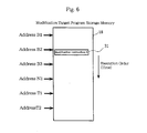
In Figure 6 the modification target program storage memory 18
contains a number 3 modification instruction 31 which loads the contents
of the modifying address storage table 19 to the modifying address register
17.
-
In Figure 7 the instruction ROM 14 contains number 1, 2, 4 and 5
modification instructions 41, 42, 44, and 45 which load the contents of the
modifying address storage table 19 to the modification source program
address register 211 for use 1 and the modification target program address
register 212 for use 1 in the modifying address register 17. The
instruction ROM 14 further includes a modification instruction X 43 which
loads the contents of the modifying address storage table 19 to the
modification source program address register 221 for use 2 and the
modification target program address register 222 for use 2 in the modifying
address register 17.
-
In Figure 8 the modifying address storage table 19 stores all of the
modification source addresses and the modification target addresses in
pairs.
-
The behavior of the program modification device will be described as
follows.
-
Assume that the addresses A1, A2, A3, M1, S1 and S2 in the
instruction ROM 14 shown in Figure 7, which are the addresses of the
modification source programs, are modified so as to execute the
modification target programs at the addresses B1, B2, B3, N1, T1, and T2
shown in Figure 8, respectively.
- (1) As shown in Figure 8, the modification source addresses and the
modification target addresses are written in pairs in the modifying address
storage table 19 so as to execute the programs at the addresses B1, B2, B3,
N1, T1 and T2 instead of the programs at the addresses A1, A2, A3, M1, S1
and S2. At the same time, the programs to be executed after the
modification are written at the corresponding addresses in the modification
target program storage memory 18. Such writing to the modifying
address storage table 19 and to the modification target program storage
memory 18 can be performed through a serial interface or from an external
CPU accessible to these units.
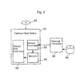
The writing is conceptually shown in Figure 9. In this illustration,
the data in a hard disk 96 are written into a memory 94 through an
external personal computer 90 and then a system controller 93 inside an
optical disk drive 91. The optical disk drive 91 drives an optical disk 95.
The memory 94 which stores modification target programs also utilizes a
part of the memory of the optical disk drive 91. According to the
modification system shown in Figure 9, it becomes possible for the
manufactures and franchised stores to upgrade the programs of games and
optical disk drives of old types already sold and their functions by using
their CPUs upon user requests.
- (2) The instruction ROM 14 has modification instructions embedded
therein when it is fabricated; however, these instructions are embedded
every predetermined number of program steps because modification
positions are not known beforehand. Assume that the modification
instructions to be loaded from the modifying address storage table 19 to a
program address register for use 1 are used as the modification
instructions to modify the programs at the addresses A1, A2, A3, S1 and S2.
Also assume that the modification instructions to be loaded from the
modifying address storage table 19 to a program address register for use 2
are used as the modification instructions to modify the programs at the
address M1.
- (3) When a device such as DVD is used, the instruction acquisition
unit 3 acquires instructions in sequence from the instruction ROM 14, and
the execution unit 2 executes the instructions.
- (4) The program monitor unit 5 keeps monitoring the addresses of the
program data acquired by the instruction acquisition unit 3 and the
addresses of the modification source program data inside the modifying
address registers 17 by referring to the modifying address storage table 19.
- (5) When the number 1 modification instruction 41 in the instruction
ROM 14 shown in Figure 7 is executed, "the address A1 and the address
B1", which is the first pair entered in the modifying address storage table
19, is loaded to the registers 211 and 212 for use 1 in the modifying address
register 17. The modifying address register 17 makes it apparent that no
address has been written, for example, by setting a maximum value
(0xFFFFFFFF for example) as the initial value. Alternatively, a flag can
be provided to indicate that no address has been written.
- (6) When the instruction acquisition unit 3 tries to acquire program
data from the address A1 in the instruction ROM 14 shown in Figure 7, the
program monitor unit 5 makes the acquired instruction switch unit 6
acquire a program from the address B1, which is the pair to the address A1
because the modification source program address in the register 211 is A1.
Consequently, the acquired instruction switch unit 6 acquires an
instruction from the address B1 in the modification target program storage
memory 18 shown in Figure 6 instead of the address A1 in the instruction
ROM 14. This indicates that the program data at the address A1 in the
instruction ROM 14 shown in Figure 4 have been modified into the
program data at the address B1 on the modification target program storage
memory 18 shown in Figure 6.
By the program data at the address B1 on the modification program
storage memory 18, the modification target program is executed, and the
execution of the program in the instruction ROM 14 is returned from a
predetermined position or portion by a jump instruction or the like. After
each modification target program (data) is executed, the program in the
instruction ROM 14 is returned in the same manner hereinafter.
- (7) When the number 2 modification instruction 42 in the instruction
ROM 14 shown in Figure 7 is executed, "the address A2 and the address
B2", which is the second pair entered in the modifying address storage
table 19, is loaded to the registers 211 and 212 for use 1 in place of the pair
"the address A1 and the address B1".
- (8) When the instruction acquisition unit 3 tries to acquire a program
from the address A2 in the instruction ROM 14 shown in Figure 4, the
program monitor unit 5 makes the acquired instruction switch unit 6
acquire a program from the address B2, which is the pair to the address A2
because the modification source program address in the register 211 is A2.
Consequently, the acquired instruction switch unit 6 acquires an
instruction from the address B2 in the modification target program storage
memory 18 shown in Figure 6 instead of the address A2 in the instruction
ROM 14. This indicates that the program data at the address A2 in the
instruction ROM 14 shown in Figure 7 have been modified into the
program data at the address B2 on the modification target program storage
memory 18 shown in Figure 6.
- (9) After the program at the address A2 in the instruction ROM 14 is
modified into the program at the address B2 on the modification program
storage memory 18 shown in Figure 6, the program at the address B2 is
executed to reach the number 3 modification instruction 31 in the
modification target program storage memory 18. Due to the execution of
this modification instruction, "the address A3 and the address B3", which is
the third pair entered in the modifying address storage table 19, is loaded
to the registers 211 and 212 for use 1 in the modifying address register 17.
- (10) When the instruction acquisition unit 3 tries to acquire a
program from the address A3 in the instruction ROM 14 shown in Figure 7,
the program monitor unit 5 makes the acquired instruction switch unit 6
acquire program data from the address B3, which is the pair to the address
A3 because the modification source program address in the register 211 is
A3. Consequently, the acquired instruction switch unit 6 acquires an
instruction not from the address A3 in the instruction ROM 14 but from
the address B3 in the modification target program storage memory 18
shown in Figure 6. This indicates that the program data at the address
A3 in the instruction ROM 14 shown in Figure 7 have been modified into
the program data at the address B3 on the modification target program
storage memory 18 shown in Figure 6.
By thus arranging the information stored in the modifying address
register 17, that is, modification instructions such as the addresses of
modification source programs on the modification target program storage
memory 18, it becomes possible to execute the modification instructions in
the other positions than positions where the modification instructions are
previously embedded in the instruction ROM 14, and to modify the
program. This can increase the number of positions to be modified as
desired.
- (11) When the X modification instruction 43 in the instruction ROM
14 shown in Figure 7 is executed, "the address M1 and the address N1",
which is the fourth pair entered in the modifying address storage table 19,
is loaded to the registers 221 and 222 for use 2 in the modifying address
register 17. In that case, the modification source program address
register 211 for use 1 and the modification target program address register
212 for use 1 are not updated because of the different use.
- (12) When the instruction acquisition unit 3 tries to acquire a
program from the address M1 in the instruction ROM 14 shown in Figure 7,
the program monitor unit 5 makes the acquired instruction switch unit 6
acquire a program from the address N1, which is the pair to the address
M1 because the modification source program address in the modification
source program address register 221 for use 2 in the modifying address
register 17 is M1. Consequently, the acquired instruction switch unit 6
acquires a program to be executed not from the address M1 in the
instruction ROM 14 but from the address N1 in the modification target
program storage memory 18 shown in Figure 6. This indicates that the
program data at the address M1 in the instruction ROM 14 shown in
Figure 7 have been modified into the program data at the address N1 on
the modification target program storage memory 18 shown in Figure 6.
The program modification is performed regardless of the value of the
register for use 1 in the modifying address register 17. For example, in
the case where the resister for use 1 is used for program modification (to
make the program bug-free), and the register for use 2 is used for
debugging (to add a program for debugging such as dumping the status of
memory or register), the modification program for debugging has effects
and advantages of being able to be fabricated independently of the
modification program for modifying bugs.
- (13) The number 4 and 5 modification instructions 44 and 45 in
Figure 7 are arranged at the heads of interrupt-service routines and of the
switch points of tasks (positions to issue system calls for example).
- (14) When the number 4 and 5 modification instructions 44 and 45 in
the instruction ROM 14 shown in Figure 7 are executed, "the address S1
and the address T1" or "the address S2 and the address T2", which are the
fifth or sixth pairs entered in the modifying address storage table 19, is
loaded to the registers 211 and 212 for use 1 instead of the addresses of the
already processed modification portions.
- (15) When the instruction acquisition unit 3 tries to acquire a
program from the address S1 in the instruction ROM 14 shown in Figure 7,
the program monitor unit 5 makes the acquired instruction switch unit 6
acquire a program from the address T1, which is the pair to the address S1
because the modification source program address in the register 211 is S1.
Consequently, the acquired instruction switch unit 6 acquires an
instruction not from the address S1 in the instruction ROM 14 but from the
address T1 in the modification target program storage memory 18 shown in
Figure 6. This indicates that the program data at the address S1 in the
instruction ROM 14 shown in Figure 7 have been modified into the
program data on the modification target program storage memory 18
shown in Figure 6. This holds true with the address S2.
-
-
The arrangement of modification instructions at the heads of
interrupt-service routines and of the switch points of tasks indicate that
modification instructions are arranged in all the heads of the positions
which operate asynchronously. By further arranging load modification
instructions together with inherent correct programs in the modification
target program storage memory 18, it becomes possible to embed
modification instructions only at the heads of interrupt-service routines
and of task switch points, which is the minimum number to be previously
embedded in the instruction ROM 14.
-
When additional modification instructions are needed, they can be
arranged on the modification target program storage memory 18 so as to
perform program modification at a necessary number of positions.
-
The interrupt-service routines and the task switch points include a
disk sync detection interrupt-service routine 61, an error correction
interrupt-service routine 62, a host transfer interrupt-service routine 63
and a main process routine 64 shown in Figure 10 in the case of an optical
disk controller. In these routines 61 to 64, the load modification
instructions 41, 42, 43 and 51 could be embedded, respectively. If
necessary, load modification instructions could be arranged on the
modification target program storage memory 18.
(EMBODIMENT 2)
-
The present embodiment relates to the execution of data modified by
the saving of a program in the process of being executed and
interrupt-service routines when an interrupt occurs, as described last in
the first embodiment.
-
Figure 11 shows a flowchart depicting the procedure in the present
embodiment.
-
In a DVD (optical disk drive), in a series of processes including
displaying digital data like images read from DVD-ROM, there are various
kinds of independent interrupts such as error (codes) correction of the read
digital data, the transfer of corrected data to the host CPU and
synchronous detection. In that case, the program data in process is saved
in every independent process, and modification instructions are previously
stored at the beginning of the program data for an interrupt process.
Consequently, in such a case where the presence of an error in the routine
of an instruction to transfer to the host CPU is found after the fabrication
of ROM has been completed, this routine can be modified exclusively.
-
At the steps a4 and a5 in Figure 11, when there is no modification in
the routine, a program in the address next to the modification instruction
is read and executed at the step a7. On the other hand, when there is a
modification, the modified program is executed at the step a6. The
execution of the modification-free program and the procedure of the
execution of the modified program at the steps a6 and a7 are the same as
those in the first embodiment, so that the description will be omitted.
-
When the process of the interrupt-service routine is finished, the
saved data are returned at the step a8 so as to resume the original process.
-
In the present embodiment, the interrupt is one step. When another
interrupt occurs during the process of the preceding interrupt, the
fundamental process does not change except that the interrupt process
becomes complicated such as data saving becoming two steps.
(EMBODIMENT 3)
-
In the present embodiment, in order to reduce the cost, the expensive
modifying address registers are exclusively used to store the addresses of
modification source program data.
-
The program modification device of the present embodiment will be
described as follows with reference to the drawings by concentrating on the
parts that differ from the first and second embodiments.
-
Figure 12 shows the conceptual illustration of the contents of a
program, which are actually written in machine language, to be executed
by the CPU core unit in the third embodiment. In the illustration, an
execution program 100 includes an address 101 and program data 102
formed in a pair. The asterisks on the addresses 3, 10 and 12 show the
presence of errors in the program data at these addresses.
-
Figure 13 shows the conceptual illustration of a memory 110 for
modification programs which also serves as a modifying address storage
table. As shown in Figure 13 at each address of the memory 110, data for
sequential modifications are stored in the order in which the modification
source programs in execution programs are executed. The data for
sequential modifications comprises a modification source program data
unit 111 which stores modification target program data obtained by
modifying the errors of the modification source program data, and the
termination identifier of the modification target program data; a next
modification preparation data unit 112 which stores the address (number)
of the next modification source program data and instructions to write this
address in the modifying address register; and a return data unit 113
which stores data for a jump to a predetermined address of the execution
data.
-
Figure 14 shows the flowchart depicting the procedure of sequentially
executing execution programs by replacing error-containing program data
with error-corrected program data. The procedure will be described as
follows with reference to Figures 12, 13 and 14.
- 1) Before starting the execution programs, the first modification
source program address (3 in Figure 12) is stored in the modifying address
register 17. Furthermore, i=1 is set at the counter (not shown) in the
acquired instruction switch unit 6. This writing and the first modification
source program address itself could be written in another memory for
initial setting. Alternatively, another instruction could be written from
the beginning under the assumption that there is a modification at the
beginning of the execution programs.
- 2) Programs are executed in descending order by address.
- 3) The program monitor unit 5 continuously checks whether or not
the address of the program data that the execution unit 2 of the CPU core
unit 1 acquires for process agrees with the address in the modifying
address register 17.
- 4) When these addresses agree with each other, the acquired
instruction switch unit 6 invokes the data at the address i (i=1 when it is
the first). Under these circumstances, error-corrected program data are
executed in place of the error-containing program data corresponding to the
modification source program address, and the address of the next
modification source program is overwritten in the modifying address
register 17 (when it is the first, "10" is written as shown in Figure 12).
Thus, the counter value becomes i=i+1 (when it starts at i=1, the value
becomes 2), and a jump takes place to the address of the program to be
executed next in the execution programs (when the modification source
program address is "3", the next address is "4").
- 5) The execution unit 2 executes execution programs in sequence.
Hereinafter, these processes are repeated for each modification source
program data.
-
-
As known from the above-mentioned description, the present
embodiment is useful when execution programs are executed in descending
order by address.
-
As a modified example of the present embodiment, it is possible to
store modification source program addresses and modification target
program address in pairs, and further store the modification target
program data in another memory. This modified example is useful when
execution programs contain branches and loops.
-
As further another modified example, it is possible to write the
identifier of a load modification instruction useful to specify a modification
target address before and after the load modification instruction in a
specified memory, and to make the program monitor unit 5 determine the
modification target address from the identifier.
-
As further another modified example, it is possible to provide a
memory for each branch of a task and to store modification target program
data and instructions involved in these program data sequentially in the
memory.
-
Moreover, modification target program data could be found, based on
the addresses 3, 10 and 12 in the address 101 shown in Figure 12 instead
of "i", and by further referring to the contents of Figure 13.
(EMBODIMENT 4)
-
In the present embodiment, the next modification target programs
are exclusively stored in a memory capable of high-speed readout.
-
Figure 15 (2) shows the structure of the program modification device
of the present embodiment. Figure 15 (1) shows the structure of an
example of the program modification device of the third embodiment.
When comparisons are made with the conventional device shown in Figure
3, the program modification device shown in Figure 15 (1) has a feature
that the expensive register 17 exclusively stores the addresses of the next
modification source programs, and the addresses of the other modification
source programs are stored in an inexpensive nonvolatile memory 70. In
contrast, the program modification device of the present embodiment
shown in Figure 15 (2) has a feature that the modification target program
corresponding to the address of the next modification source program is
exclusively stored in a memory 73 capable of high-speed readout in
addition to the storage of the address of the next modification source
program to the register 17. This feature realizes the further speedups of
program processing, thereby increasing the effects of the present invention
on some kinds of device system.
-
Although the present invention has been described so far based on the
embodiments, the device of the invention is not restricted to the above
description, and further includes the following features.
- 1) Like the conventional device, the device of the present invention
has an indirect call table.
- 2) The register which stores various types of instructions delivers its
performance by dividing it into several portions. In other words, the
register is plural in terms of use, but is physically and mechanically one.
- 3) The register for various load modification instructions can be
replaced by other types of registers.
- 4) The modification of a program can be the upgrading of programs
instead of error correction. Alternatively, various modification
instructions are integrated into the device in expectation of the contents to
be upgraded in a program.
- 5) As mentioned in the fourth embodiment, the memory for
modification target program data has a multi-step structure and the
acquired instruction switch unit is a kind of selector. They may have
structures different from the structures described in the claims of the
present invention or may be subjected to other processes; however, the
actions and effects based on the structures in the claims of the present
invention can be substantially obtained.
-
INDUSTRIAL APPLICABILITY
-
As will be understood from the aforementioned description, the
present invention makes it possible to perform error correction at any
positions in an execution program or to perform modification for upgrading,
with the use of a little hardware (modifying address register).
-
These effects are remarkable when the inventions of claims 5 and 6
are applied to the heads of task switch points of a demodulating process, an
error correcting process, a data transfer process to the host personal
computer in programs such as a servo-controlled process and a data error
correcting process in a DVD drive.
-
In a field where upgrading occurs at high speed, a CPU system
containing programs of old versions can be changed into an upgraded CPU
system only by adding a few memories for modification. Therefore, in
same cases, it is possible to perform modifications of old programs and data
in order to make them operate or display. As a result, while users can
purchase modified programs or data only, the manufactures make it a
selling point when they sell devices in a field where upgrading in programs
occurs at high speed.