EP1111344A1 - Sensor fault detection method and apparatus - Google Patents
Sensor fault detection method and apparatus Download PDFInfo
- Publication number
- EP1111344A1 EP1111344A1 EP00311374A EP00311374A EP1111344A1 EP 1111344 A1 EP1111344 A1 EP 1111344A1 EP 00311374 A EP00311374 A EP 00311374A EP 00311374 A EP00311374 A EP 00311374A EP 1111344 A1 EP1111344 A1 EP 1111344A1
- Authority
- EP
- European Patent Office
- Prior art keywords
- voltage
- window
- common mode
- circuit
- bridge
- Prior art date
- Legal status (The legal status is an assumption and is not a legal conclusion. Google has not performed a legal analysis and makes no representation as to the accuracy of the status listed.)
- Granted
Links
- 238000001514 detection method Methods 0.000 title claims abstract description 26
- 238000000034 method Methods 0.000 claims description 18
- 239000003990 capacitor Substances 0.000 claims description 9
- 238000012544 monitoring process Methods 0.000 claims description 3
- 229920005994 diacetyl cellulose Polymers 0.000 description 12
- 230000008859 change Effects 0.000 description 6
- 230000003750 conditioning effect Effects 0.000 description 6
- 230000035945 sensitivity Effects 0.000 description 3
- 230000001133 acceleration Effects 0.000 description 2
- 239000000446 fuel Substances 0.000 description 2
- 230000006870 function Effects 0.000 description 2
- 238000002347 injection Methods 0.000 description 2
- 239000007924 injection Substances 0.000 description 2
- 230000007257 malfunction Effects 0.000 description 2
- 230000004048 modification Effects 0.000 description 2
- 238000012986 modification Methods 0.000 description 2
- 230000004044 response Effects 0.000 description 2
- 238000009966 trimming Methods 0.000 description 2
- 101100204393 Arabidopsis thaliana SUMO2 gene Proteins 0.000 description 1
- 101150112492 SUM-1 gene Proteins 0.000 description 1
- 101150096255 SUMO1 gene Proteins 0.000 description 1
- 101100311460 Schizosaccharomyces pombe (strain 972 / ATCC 24843) sum2 gene Proteins 0.000 description 1
- 238000013459 approach Methods 0.000 description 1
- 230000008569 process Effects 0.000 description 1
- 238000012216 screening Methods 0.000 description 1
- 229910052710 silicon Inorganic materials 0.000 description 1
- 239000010703 silicon Substances 0.000 description 1
- 239000000758 substrate Substances 0.000 description 1
Images





Classifications
-
- G—PHYSICS
- G01—MEASURING; TESTING
- G01D—MEASURING NOT SPECIALLY ADAPTED FOR A SPECIFIC VARIABLE; ARRANGEMENTS FOR MEASURING TWO OR MORE VARIABLES NOT COVERED IN A SINGLE OTHER SUBCLASS; TARIFF METERING APPARATUS; MEASURING OR TESTING NOT OTHERWISE PROVIDED FOR
- G01D18/00—Testing or calibrating apparatus or arrangements provided for in groups G01D1/00 - G01D15/00
-
- G—PHYSICS
- G01—MEASURING; TESTING
- G01D—MEASURING NOT SPECIALLY ADAPTED FOR A SPECIFIC VARIABLE; ARRANGEMENTS FOR MEASURING TWO OR MORE VARIABLES NOT COVERED IN A SINGLE OTHER SUBCLASS; TARIFF METERING APPARATUS; MEASURING OR TESTING NOT OTHERWISE PROVIDED FOR
- G01D3/00—Indicating or recording apparatus with provision for the special purposes referred to in the subgroups
- G01D3/02—Indicating or recording apparatus with provision for the special purposes referred to in the subgroups with provision for altering or correcting the law of variation
- G01D3/022—Indicating or recording apparatus with provision for the special purposes referred to in the subgroups with provision for altering or correcting the law of variation having an ideal characteristic, map or correction data stored in a digital memory
-
- G—PHYSICS
- G01—MEASURING; TESTING
- G01D—MEASURING NOT SPECIALLY ADAPTED FOR A SPECIFIC VARIABLE; ARRANGEMENTS FOR MEASURING TWO OR MORE VARIABLES NOT COVERED IN A SINGLE OTHER SUBCLASS; TARIFF METERING APPARATUS; MEASURING OR TESTING NOT OTHERWISE PROVIDED FOR
- G01D3/00—Indicating or recording apparatus with provision for the special purposes referred to in the subgroups
- G01D3/08—Indicating or recording apparatus with provision for the special purposes referred to in the subgroups with provision for safeguarding the apparatus, e.g. against abnormal operation, against breakdown
Definitions
- This invention relates generally to condition responsive sensors having a full bridge circuit such as a bridge circuit comprising piezoresistive elements and more particularly to apparatus and methods for providing fault detection which enables detection of errors in either the offset or sensitivity of a sensor that can be smaller than a full scale output signal.
- Bridge circuit sensors are widely used to sense a change in a certain condition, such as a change in pressure or a change in acceleration.
- a common bridge circuit sensor comprises piezoresistive elements mounted on a substrate, such as silicon, so that changes in the sensed condition causes a change in stress induced in the several piezoresistive elements to provide an output of the bridge which is a function of the change in the sensed condition.
- Typical uses include acceleration sensors for use in automotive braking systems and pressure sensors for use in automotive fuel injection systems, by way of example.
- An object of the present invention is the provision of a method and circuit for detecting faults in a bridge circuit sensor simpler and more cost effective than the above noted prior art.
- Another object of the invention is the provision of an in-range fault protection system for providing an alarm whenever a fault occurs in a full bridge sensor.
- Yet another object of the invention is the provision of an in-range fault protection system for a full wheatstone piezoresistive bridge type sensor suitable for fabricating in the form of an integrated circuit which is reliable yet low in cost.
- Yet another object of the invention is the provision of such a system which can be used for other full bridge arrangements, such as a bridge containing capacitive elements.
- the common mode voltage of the full bridge outputs is defined as the voltage equal to a linear combination of the bridge output voltages which is insensitive to stimulus applied to the full bridge and is within the voltage range between the two bridge outputs. Circuit parameters to obtain the common mode voltage and fault window may be appropriately adjusted and stored in nonvolatile memory.
- the circuit to yield the common mode voltage signal may be adjustable.
- the circuit to yield the common mode voltage signal comprises a potentiometer resistor string.
- the circuit to yield the common mode voltage signal comprises at least one adjustable capacitor.
- the circuit to yield the common mode voltage signal may comprise at least one capacitive Digital-to-Analogue-Converter.
- the voltage window is defined by a circuit for adding and subtracting a window width voltage from a window centering voltage where the window centering voltage and window width voltages are proportional to the bridge supply voltage. More preferably, the fault detection apparatus further comprises a circuit for adjusting the window centering voltage in a compensating manner with temperature. The fault detection apparatus may further comprise a circuit for adjusting the window width voltage in a compensating manner with temperature. Preferably, the window width voltage is proportional to the full scale output signal.
- the common mode voltage signal may be an analog signal and the fault detecting apparatus may further comprise a circuit for digitising the analog signal and window parameters and performing calculations in the digital domain on digitised values of the common mode voltage signal and window parameters to determine a fault condition.
- the common mode voltage signal may be derived from a first analog signal, from a first output node of the full wheatstone bridge, and from a second analog signal, from a second output node of the full wheatstone bridge, and the fault detection apparatus may further comprise a circuit for digitising the first analog signal, a circuit for digitising the second analog signal, a circuit for digistising parameters of the voltage window and a circuit for performing calculations in the digital domain on digitised values of the first analog signal and the second analog signal to form the common mode voltage signal and on the common mode voltage signal and digitised values of the window parameters to determine a fault condition.
- the full wheatstone bridge comprises piezoresistive elements.
- a method for monitoring faults of a full wheatstone bridge sensor element and connections thereto, the sensor elements having bridge outputs comprising the steps of:
- the fault window is defined by a voltage range defined by a window centering voltage and a window width voltage which are both proportional to the bridge supply voltage.
- the window centering voltage is equal to the common mode voltage at the time of sensor calibration.
- the fault window is defined between the window centering voltage minus the window width voltage to the window centering voltage plus the window width voltage.
- the window width voltage is proportional to the full scale output of the full wheatstone bridge.
- the common mode voltage is fixed to equal the average of the bridge output voltages.
- the bridge sensor element is supplied with a voltage source.
- the bridge sensor element is supplied with a voltage source through a series resistor.
- the bridge sensor element may be supplied with a current source.
- a piezoresistive sensor conditioner application specific, integrated circuit (ASIC) 10 is shown along with a piezoresistive sensor element 12 made in accordance with a preferred embodiment of the invention.
- ASIC 10 will convert small changes in the off-chip piezoresistors of sensor element 12 to large changes in the ASIC supply-ratiometric output voltage.
- piezoresistors R1-R4 are arranged in a full wheatstone bridge, in externally connected sensing element 12. The value of resistors R1-R4 vary in response to the application of a mechanical stimulus such as pressure used in various applications including automotive under-hood applications such as fuel injection systems.
- ASIC 10 has nodes BRG, INP, INM, and RTN for connection to nodes of sensor element 12 in turn connected to resistors R1-R4 of sensor element 12 as well as nodes PWR, OUT, and RTN for external connection of power and the sensor output.
- common mode voltage, V CM is obtained using a circuit portion 13 connected between the bridge voltage output connections INP, INM.
- voltage V CM is equal to A*V INP +(1-A)*V INM .
- circuit portion 13 comprises a first DAC made up of resistors R11, R12 and R13.
- a fault windowing centering voltage, C*V BRG is obtained using a circuit portion 14 in the form of a second DAC made up of resistors R8, R9 and R10 and a fault parameter window width parameter, W*V BRG , is obtained using a third circuit portion 15 in the form of a third DAC made up of resistors R5, R6 and R7.
- the values of A, C and W are stored in nonvolatile memory 16.
- the output of circuit portions 13, 14 and 15 are connected to window comparator 18, to be discussed below, in order to obtain an indication of the status of a fault condition.
- C*V BRG Fault window centering voltage, proportional to the bridge supply voltage V BRG . is adjusted to be nearly equal to the common mode voltage V CM following common mode voltage trimming.
- Fault window width parameter W*V BRG is adjusted to equal a known fraction of the bridge supply voltage.
- the fault window width parameter can be made equal to a known fraction of the full scale output.
- the window width parameter, W is typically adjusted to be as small as possible to maximize fault detectivity.
- the lower limit of the window width parameter is selected to be sufficiently larger than the expected variations in common mode voltage not compensated for during sensor calibration as well as ASIC influences such as calibration error and drift.
- Calibration adjustments requiring thermal compensation involve repeating the calibration process at multiple temperatures to set linear and higher order thermal coefficients of compensation. All adjustable parameters are stored in nonvolatile memory 16. Sensors requiring thermal compensation may derive a temperature signal either from a conventional temperature reference on the ASIC 10 as indicated in Fig. 2a, to be discussed, (e.g., a signal related to a bandgap reference voltage) or by a signal related to the sense element temperature.
- One method to obtain a signal related to the sensor element temperature is to power the sensor element as shown in either Figs. 3a or 3b and use the temperature variation in V BRG , due to the sensor bridge resistance temperature dependence, as the temperature signal.
- a series resistance, R SERIES is provided having significantly lower thermal variation than the full bridge resistance would cause the bridge voltage V BRG to vary over temperature mainly due to the resistance change in the full bridge resistance.
- a current source, I SOURCE is provided having significantly lower thermal variation than the full bridge resistance would cause the bridge voltage, V BRG to vary over temperature mainly due to the full bridge resistance thermal variation.
- the bridge powering techniques shown in figures 3a and 3b reduce the sensor element 12 signal by the fraction of V BRG /V PWR .
- Embodiments not deriving the temperature signal from the sensor element may employ the bridge powering technique shown in figure 3 to maximize sensor signal thereby reducing required ASIC gain.
- the common mode voltage of the two bridge halves is obtained at circuit portion 13 comprising an adjustable resistor divider tap or first potentiometric DAC output which is serially connected between the bridge output nodes.
- Circuit portion 14 comprising the second DAC connected between the bridge voltage V BRG and analog ground V RTN , is adjusted to center the fault window and satisfy the relation V C ⁇ V CM .
- Circuit portion 15 comprising the third DAC, connected between the bridge voltage and analog ground, is set to yield half the fault window width.
- the parameter W*V BRG is then added to C*V BRG at a first summing circuit SUM1 and in turn inputted to the positive input of the first comparator Q1 and subtracted from C*V BRG at a second summing circuit SUM2 and in turn inputted to the negative input of the second comparator Q2.
- the outputs of the comparators Q1and Q2 are connected to the inputs of a digital logic OR gate Q3 so that if the common mode voltage falls outside the window bounded by (C - W)*V BRG to (C + W)*V BRG a fault is indicated by a logic "1" output of the OR gate Q3.
- the output of the OR gate Q3 reflects the status of the fault condition so that the user is alerted to a malfunction of the sensor element or its connectivity to the ASIC.
- the above embodiment may be further simplified by eliminating certain ASIC adjustments to the common mode fault parameters by carefully controlling or screening bridge parameters which influence the stimulus, time and temperature variability of the bridge common mode voltage.
- the resistive DAC of circuit portion 13 used to yield the common mode voltage may be replaced by a pair of equal valued resistors (not shown) between the full bridge outputs if the stimulus sensitivities of the two half bridges are matched sufficiently well.
- circuit portion 13 can comprise first and second capacitive DACs C11, C12 coupled to a comparator Q4 to provide common mode voltage V CM .
- Memory 16 has ports n - A0, A1, A2,...An; m - C0, C1, C2...Cm; p - W0, W1, W2,...Wp interconnected with temperature conditioning circuit 20. Thermal compensation for the window centering voltage may be eliminated by careful control of sense element parameters which affect the common mode voltage over temperature.
- the window width voltage may be inversely proportional to ASIC gain.
- the thermal compensation coefficients for the window width parameter may be functionally related to the sensor's stimulus gain thermal compensation coefficients, thereby providing a window setting given by a known fraction of full scale output over a defined temperature range.
- digitized analog signals related to the full bridge output and supply voltages can be employed. The digitized data are then evaluated to determine the presence of a fault condition caused by changes in the common mode voltage of the full bridge.
- conditioning circuit 22 and analog to digital converter 24, connected between voltage V BRG and common are connected to voltage V BRG and provide a digitized signal at X which is inputted to microcontroller 34.
- Conditioning circuit 26 and analog to digital converter 28, connected between voltage V BRG and common are connected to voltage V INP and provide a digitized signal at Y which is inputted to microcontroller 34.
- conditioning circuit 30 and analog to digital converter 32 connected between voltage V BRG and common, are connected to voltage V INM and provide a digitized signal at Z which is inputted to microcontroller 34.
- capacitive dividers and capacitive DACs may be used to generate the necessary signals related to the full bridge voltages.
- One method to provide generation of the V CM signal using a pair of capacitive DACs comprises hardware and clocking as follows; simultaneously close a pair of switches S1 and S2, while switches S3 and S4 are open, with a clock signal ⁇ 1 to store the bridge output voltages V INP and V INM on adjustable capacitors C11 and C12, respectively.
- clock phase ⁇ 1 opens switches S1 and S2 between the bridge and capacitors and a brief period later clock signal ⁇ 2 simultaneously closes a pair of switches, S3 and S4 to store V CM onto a sample and hold circuit given by a capacitor C13 and an amplifier Q4 in a buffer feedback configuration
- the value of capacitor C13 with respect to adjustable capacitors C11 and C12 influences circuit response time.
- the adjustable capacitors C11 and C12 should be adjusted to yield V CM which is insensitive to stimulus applied to the bridge. If desired, only one of C11 or C12 needs to be made adjustable to accommodate the required V CM trimming. Also, it is obvious and within the purview of the invention to employ a non-unity gain to the amplifier Q4.
Landscapes
- Physics & Mathematics (AREA)
- General Physics & Mathematics (AREA)
- Engineering & Computer Science (AREA)
- Technology Law (AREA)
- Measuring Instrument Details And Bridges, And Automatic Balancing Devices (AREA)
- Arrangements For Transmission Of Measured Signals (AREA)
- Transmission And Conversion Of Sensor Element Output (AREA)
- Measuring Fluid Pressure (AREA)
- Indication And Recording Devices For Special Purposes And Tariff Metering Devices (AREA)
Abstract
Description
- This invention relates generally to condition responsive sensors having a full bridge circuit such as a bridge circuit comprising piezoresistive elements and more particularly to apparatus and methods for providing fault detection which enables detection of errors in either the offset or sensitivity of a sensor that can be smaller than a full scale output signal.
- Bridge circuit sensors are widely used to sense a change in a certain condition, such as a change in pressure or a change in acceleration. A common bridge circuit sensor comprises piezoresistive elements mounted on a substrate, such as silicon, so that changes in the sensed condition causes a change in stress induced in the several piezoresistive elements to provide an output of the bridge which is a function of the change in the sensed condition. Typical uses include acceleration sensors for use in automotive braking systems and pressure sensors for use in automotive fuel injection systems, by way of example. There is a continuing need, in many applications, to minimize costs associated with the sensors while at the same time providing detectivity of sensor flaws which can result in an erroneous in-range sensor output. It is known to use redundant sensors to add to the reliability of a system; however, this adds to the cost of the system. It is desired to provide a single sensor system in which the user is alerted in the event of a malfunction of sensor operation.
- In PCT application, International publication number WO99/01777, dated 14 January 1999, a circuit is disclosed for monitoring the function of a full wheatstone piezoresistive sensor bridge circuit. If the compared signals deviate by more than an acceptable amount the output of a window comparator provides an alarm signal. The disclosed circuit monitors to some extent the bridge resistors as well as the connectivity to an ASIC. However, the cited prior art is complex and is relatively expensive due to its implementation size. The approach in the cited prior art requires two separate conditioning circuits which must be precisely adjusted and stable over time and temperature.
- An object of the present invention is the provision of a method and circuit for detecting faults in a bridge circuit sensor simpler and more cost effective than the above noted prior art. Another object of the invention is the provision of an in-range fault protection system for providing an alarm whenever a fault occurs in a full bridge sensor. Yet another object of the invention is the provision of an in-range fault protection system for a full wheatstone piezoresistive bridge type sensor suitable for fabricating in the form of an integrated circuit which is reliable yet low in cost. Yet another object of the invention is the provision of such a system which can be used for other full bridge arrangements, such as a bridge containing capacitive elements.
- Briefly described, a fault detection system made in accordance with one aspect of the invention comprises circuitry connected to the outputs of an energized full wheatstone bridge to provide a means to generate a common mode voltage of the bridge outputs during sensor calibration which is then compared to a voltage window to determine a fault status during normal operation. The common mode voltage of the full bridge outputs is defined as the voltage equal to a linear combination of the bridge output voltages which is insensitive to stimulus applied to the full bridge and is within the voltage range between the two bridge outputs. Circuit parameters to obtain the common mode voltage and fault window may be appropriately adjusted and stored in nonvolatile memory.
- According to the invention there is provided fault detection apparatus for a full wheatstone bridge comprising a circuit connected between output nodes of the full wheatstone bridge to obtain a common mode voltage signal insensitive to stimulus, a circuit for providing a predetermined voltage window and a circuit for comparing the common mode voltage to a voltage window to determine a sensor fault condition.
- The circuit to yield the common mode voltage signal may be adjustable. Preferably, the circuit to yield the common mode voltage signal comprises a potentiometer resistor string. Alternatively, the circuit to yield the common mode voltage signal comprises at least one adjustable capacitor. The circuit to yield the common mode voltage signal may comprise at least one capacitive Digital-to-Analogue-Converter.
- Preferably, the voltage window is defined by a circuit for adding and subtracting a window width voltage from a window centering voltage where the window centering voltage and window width voltages are proportional to the bridge supply voltage. More preferably, the fault detection apparatus further comprises a circuit for adjusting the window centering voltage in a compensating manner with temperature. The fault detection apparatus may further comprise a circuit for adjusting the window width voltage in a compensating manner with temperature. Preferably, the window width voltage is proportional to the full scale output signal.
- The common mode voltage signal may be an analog signal and the fault detecting apparatus may further comprise a circuit for digitising the analog signal and window parameters and performing calculations in the digital domain on digitised values of the common mode voltage signal and window parameters to determine a fault condition.
- The common mode voltage signal may be derived from a first analog signal, from a first output node of the full wheatstone bridge, and from a second analog signal, from a second output node of the full wheatstone bridge, and the fault detection apparatus may further comprise a circuit for digitising the first analog signal, a circuit for digitising the second analog signal, a circuit for digistising parameters of the voltage window and a circuit for performing calculations in the digital domain on digitised values of the first analog signal and the second analog signal to form the common mode voltage signal and on the common mode voltage signal and digitised values of the window parameters to determine a fault condition.
- Preferably, the full wheatstone bridge comprises piezoresistive elements. Also according to the invention there is provided a method for monitoring faults of a full wheatstone bridge sensor element and connections thereto, the sensor elements having bridge outputs, comprising the steps of:
- energising the bridge sensor element with a power source,
- adjusting a circuit between the outputs of the full wheatstone bridge sensor element to yield a common mode voltage signal, which is equal to a linear combination of the bridge output voltages and is insensitive to stimulus during sensor calibration,
- storing the adjusted circuit parameters in memory for setting the common mode voltage,
- comparing the common mode voltage to a fault window; and
- setting a fault indication whenever the common mode voltage exceeds the fault window.
-
- Preferably, the fault window is defined by a voltage range defined by a window centering voltage and a window width voltage which are both proportional to the bridge supply voltage. Preferably, the window centering voltage is equal to the common mode voltage at the time of sensor calibration. Preferably, the fault window is defined between the window centering voltage minus the window width voltage to the window centering voltage plus the window width voltage.
- Preferably, the window width voltage is proportional to the full scale output of the full wheatstone bridge.
- Preferably, the common mode voltage is fixed to equal the average of the bridge output voltages.
- Preferably, the bridge sensor element is supplied with a voltage source. Preferably, the bridge sensor element is supplied with a voltage source through a series resistor. Alternatively, the bridge sensor element may be supplied with a current source.
- Other objects, advantages and details of the sensor of the invention and method for providing in-range fault detection appear in the following detailed description of preferred embodiments of the invention, the detailed description referring to the following drawings in which:
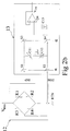
- Fig. 1 is a schematic of a full wheatstone bridge sensor element and an ASIC embodying a circuit made in accordance with the invention;
- Fig. 2 is a schematic of the common mode fault detection circuit portion of the Fig. 1 ASIC showing circuit portions for providing common mode voltage, window centering voltage and window width voltage, and a window comparator circuit;
- Fig. 2a is a schematic of a modification of the Fig. 2 structure which includes a temperature compensation circuit for the common mode voltage, window centering voltage and window width voltage;
- Fig. 2b is a schematic of the common mode voltage circuit portion of the common mode fault detection circuit portion of Fig. 2 showing an alternate embodiment of the invention using capacitive DACs for obtaining the common mode voltage;
- Fig. 2c is a schematic similar to Fig. 2a of a modified embodiment employing analog to digital converters to perform calculations in the digital domain;
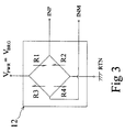
- Fig. 3 is a schematic of a portion of the Fig. 1 ASIC showing the full bridge sensor element power source as a voltage source;
- Fig. 3a is a schematic similar to Fig. 3 showing the full bridge sensor element power source as a voltage source and a series resistor; and
- Fig. 3b is a schematic similar to Fig. 3 showing the full bridge sensor element power source as a current source.
-
- With reference to Fig. 1, a piezoresistive sensor conditioner application specific, integrated circuit (ASIC) 10 is shown along with a
piezoresistive sensor element 12 made in accordance with a preferred embodiment of the invention.ASIC 10 will convert small changes in the off-chip piezoresistors ofsensor element 12 to large changes in the ASIC supply-ratiometric output voltage. Four piezoresistors R1-R4 are arranged in a full wheatstone bridge, in externally connectedsensing element 12. The value of resistors R1-R4 vary in response to the application of a mechanical stimulus such as pressure used in various applications including automotive under-hood applications such as fuel injection systems.ASIC 10 has nodes BRG, INP, INM, and RTN for connection to nodes ofsensor element 12 in turn connected to resistors R1-R4 ofsensor element 12 as well as nodes PWR, OUT, and RTN for external connection of power and the sensor output. - In accordance with the preferred embodiment of the invention, common mode voltage, VCM, is obtained using a
circuit portion 13 connected between the bridge voltage output connections INP, INM. As will be explained in greater detail below, voltage VCM is equal to A*VINP+(1-A)*VINM. In the Fig. 2 embodiment,circuit portion 13 comprises a first DAC made up of resistors R11, R12 and R13. A fault windowing centering voltage, C*VBRG, is obtained using acircuit portion 14 in the form of a second DAC made up of resistors R8, R9 and R10 and a fault parameter window width parameter, W*VBRG, is obtained using athird circuit portion 15 in the form of a third DAC made up of resistors R5, R6 and R7. The values of A, C and W are stored innonvolatile memory 16. The output ofcircuit portions window comparator 18, to be discussed below, in order to obtain an indication of the status of a fault condition. - The fault detection system is calibrated by first adjusting the common mode voltage, VCM to be insensitive to applied stimulus to the full bridge equal to a linear combination of the full bridge output voltages VINP, VINM bounded by the full bridge output voltages (i.e., VCM = {A VINP +(1-A) VINM}, where 0 < A < 1 and VCM ≠ f(stimulus)). Perfect matching of the stimulus sensitivities of the two half bridges results in the common mode voltage being equal to the average of the two half bridge outputs (i.e., VCM = (VINP + VINM)/2; A = 0.50).
- Fault window centering voltage, C*VBRG, proportional to the bridge supply voltage VBRG. is adjusted to be nearly equal to the common mode voltage VCM following common mode voltage trimming.
- Fault window width parameter W*VBRG is adjusted to equal a known fraction of the bridge supply voltage. Alternatively, if desired, the fault window width parameter can be made equal to a known fraction of the full scale output. The window width parameter, W is typically adjusted to be as small as possible to maximize fault detectivity. In order to avoid false fault reporting over time, temperature, and the like, the lower limit of the window width parameter is selected to be sufficiently larger than the expected variations in common mode voltage not compensated for during sensor calibration as well as ASIC influences such as calibration error and drift.
- Calibration adjustments requiring thermal compensation involve repeating the calibration process at multiple temperatures to set linear and higher order thermal coefficients of compensation. All adjustable parameters are stored in
nonvolatile memory 16. Sensors requiring thermal compensation may derive a temperature signal either from a conventional temperature reference on theASIC 10 as indicated in Fig. 2a, to be discussed, (e.g., a signal related to a bandgap reference voltage) or by a signal related to the sense element temperature. One method to obtain a signal related to the sensor element temperature is to power the sensor element as shown in either Figs. 3a or 3b and use the temperature variation in VBRG, due to the sensor bridge resistance temperature dependence, as the temperature signal. As shown in figure 3a, a series resistance, RSERIES is provided having significantly lower thermal variation than the full bridge resistance would cause the bridge voltage VBRG to vary over temperature mainly due to the resistance change in the full bridge resistance. Similarly, as shown in figure 3b, a current source, ISOURCE is provided having significantly lower thermal variation than the full bridge resistance would cause the bridge voltage, VBRG to vary over temperature mainly due to the full bridge resistance thermal variation. However, the bridge powering techniques shown in figures 3a and 3b reduce thesensor element 12 signal by the fraction of VBRG/VPWR. Embodiments not deriving the temperature signal from the sensor element may employ the bridge powering technique shown in figure 3 to maximize sensor signal thereby reducing required ASIC gain. - As noted above, during operation of a calibrated fault detection system made in accordance with a preferred embodiment of the invention, the common mode voltage of the two bridge halves is obtained at
circuit portion 13 comprising an adjustable resistor divider tap or first potentiometric DAC output which is serially connected between the bridge output nodes. The setting, A of the first DAC having an output VCM = {A*VINP + (1-A)* VINM} is selected such that the common mode voltage is insensitive to applied stimulus to the full bridge.Circuit portion 14 comprising the second DAC connected between the bridge voltage VBRG and analog ground VRTN, is adjusted to center the fault window and satisfy the relation VC ~ VCM. Circuit portion 15 comprising the third DAC, connected between the bridge voltage and analog ground, is set to yield half the fault window width. The parameter W*VBRG is then added to C*VBRG at a first summing circuit SUM1 and in turn inputted to the positive input of the first comparator Q1 and subtracted from C*VBRG at a second summing circuit SUM2 and in turn inputted to the negative input of the second comparator Q2. The outputs of the comparators Q1and Q2 are connected to the inputs of a digital logic OR gate Q3 so that if the common mode voltage falls outside the window bounded by (C - W)*VBRG to (C + W)*VBRG a fault is indicated by a logic "1" output of the OR gate Q3. The output of the OR gate Q3 reflects the status of the fault condition so that the user is alerted to a malfunction of the sensor element or its connectivity to the ASIC. - The above embodiment may be further simplified by eliminating certain ASIC adjustments to the common mode fault parameters by carefully controlling or screening bridge parameters which influence the stimulus, time and temperature variability of the bridge common mode voltage. For example, the resistive DAC of
circuit portion 13 used to yield the common mode voltage may be replaced by a pair of equal valued resistors (not shown) between the full bridge outputs if the stimulus sensitivities of the two half bridges are matched sufficiently well. - Alternatively, as shown in Fig. 2b,
circuit portion 13 can comprise first and second capacitive DACs C11, C12 coupled to a comparator Q4 to provide common mode voltage VCM. - With reference to Fig. 2a, a modified embodiment includes thermal compensation provided by
temperature conditioning circuit 20 in which A is equal to A0+1*(T-T0)/T0+A2*[(T-T0)/T0]^2 +...An* [(T-T0/T0]^n; C=C0+C1*(T-T0)/T0+C2*[T-T0)/T0]^2+...(m[T-T0)/T0]^m; and W=W0+W1*(T-T0)/T0+W2*[T-T0/T0)T0]^ 2+...+Wp*[(T-T0)/T0]^p.Memory 16 has ports n - A0, A1, A2,...An; m - C0, C1, C2...Cm; p - W0, W1, W2,...Wp interconnected withtemperature conditioning circuit 20. Thermal compensation for the window centering voltage may be eliminated by careful control of sense element parameters which affect the common mode voltage over temperature. - Although a fraction of the bridge supply voltage has been used to provide the centering voltage and the windowing values, as noted above, it is within the purview of the invention to derive the window width values from the full scale span. Thus, the window width voltage may be inversely proportional to ASIC gain. During sensor calibration, the thermal compensation coefficients for the window width parameter may be functionally related to the sensor's stimulus gain thermal compensation coefficients, thereby providing a window setting given by a known fraction of full scale output over a defined temperature range.
- In another modified embodiment, digitized analog signals related to the full bridge output and supply voltages can be employed. The digitized data are then evaluated to determine the presence of a fault condition caused by changes in the common mode voltage of the full bridge. With reference to Fig. 2c,
conditioning circuit 22 and analog todigital converter 24, connected between voltage VBRG and common, are connected to voltage VBRG and provide a digitized signal at X which is inputted tomicrocontroller 34.Conditioning circuit 26 and analog todigital converter 28, connected between voltage VBRG and common, are connected to voltage VINP and provide a digitized signal at Y which is inputted tomicrocontroller 34. Similarly,conditioning circuit 30 and analog todigital converter 32, connected between voltage VBRG and common, are connected to voltage VINM and provide a digitized signal at Z which is inputted tomicrocontroller 34. The microcontroller performs calculations based on the inputs from X, Y and Z along with values from memory 16: n - A0, A1, A2,...An; m - C0, C1, C2,...Cm; p - W0, W1, W2...Wp according to the following: - It is within the scope of the invention, as shown in figure 2b that capacitive dividers and capacitive DACs may be used to generate the necessary signals related to the full bridge voltages. One method to provide generation of the VCM signal using a pair of capacitive DACs comprises hardware and clocking as follows; simultaneously close a pair of switches S1 and S2, while switches S3 and S4 are open, with a clock signal 1 to store the bridge output voltages VINP and VINM on adjustable capacitors C11 and C12, respectively. Following the settling of the voltages on adjustable capacitors C11 and C12, clock phase 1 opens switches S1 and S2 between the bridge and capacitors and a brief period later clock signal 2 simultaneously closes a pair of switches, S3 and S4 to store VCM onto a sample and hold circuit given by a capacitor C13 and an amplifier Q4 in a buffer feedback configuration The value of capacitor C13 with respect to adjustable capacitors C11 and C12 influences circuit response time. The adjustable capacitors C11 and C12 should be adjusted to yield VCM which is insensitive to stimulus applied to the bridge. If desired, only one of C11 or C12 needs to be made adjustable to accommodate the required VCM trimming. Also, it is obvious and within the purview of the invention to employ a non-unity gain to the amplifier Q4.
- It should be understood that although a particular embodiment of the invention has been described by way of illustrating the invention, the invention includes all modifications and equivalents of the disclosed embodiment falling within the scope of the appended claims.
Claims (21)
- Fault detection apparatus for a full wheatstone bridge comprising a circuit connected between output nodes of the full wheatstone bridge to obtain a common mode voltage signal insensitive to stimulus, a circuit for providing a predetermined voltage window and a circuit for comparing the common mode voltage to a voltage window to determine a sensor fault condition.
- Fault detection apparatus according to claim 1, in which the circuit to yield the common mode voltage signal is adjustable.
- Fault detection apparatus according to claim 2, in which the circuit to yield the common mode voltage signal comprises a potentiometer resistor string.
- Fault detection apparatus according to claim 2, in which the circuit to yield the common mode voltage signal comprises at least one adjustable capacitor.
- Fault detection apparatus according to claim 4, in which the circuit to yield the common mode voltage signal comprises at least one capacitive Digital-to-Analogue - Converter.
- Fault detection apparatus according to any preceding claim, in which the voltage window is defined by a circuit for adding and subtracting a window width voltage from a window centering voltage where the window centering voltage and window width voltages are proportional to the bridge supply voltage.
- Fault detection apparatus according to claim 6, further comprising a circuit for adjusting the window centering voltage in a compensating manner with temperature.
- Fault detection apparatus according to claim 6 or claim 7, further comprising a circuit for adjusting the window width voltage in a compensating manner with temperature.
- Fault detection apparatus according to any of claims 5 to 8, in which the window width voltage is proportional to the full scale output signal.
- Fault detection apparatus according to any preceding claim, in which the common mode voltage signal is an analog signal and further comprising a circuit for digitising the analog signal and window parameters and performing calculations in the digital domain on digitised values of the common mode voltage signal and window parameters to determine a fault condition.
- Fault detection apparatus according to any of claims 1 to 9, in which the common mode voltage signal is derived from a first analog signal, from a first output node of the full wheatstone bridge, and from a second analog signal, from a second output node of the full wheatstone bridge, and further comprising a circuit for digitising the first analog signal, a circuit for digitising the second analog signal, a circuit for digitising parameters of the voltage window and a circuit for performing calculations in the digital domain on digitised values of the first analog signal and the second analog signal to form the common mode voltage signal and on the common mode voltage signal and digitised values of the window parameters to determine a fault condition.
- Fault detection apparatus according to any preceding claim, in which the full wheatstone bridge comprises piezoresistive elements.
- A method for monitoring faults of a full wheatstone bridge sensor element and connections thereto, the sensor elements having bridge outputs, comprising the steps of:energising the bridge sensor element with a power source,adjusting a circuit between the outputs of the full wheatstone bridge sensor element to yield a common mode voltage signal, which is equal to a linear combination of the bridge output voltages and is insensitive to stimulus during sensor calibration,storing the adjusted circuit parameters in memory for setting the common mode voltage,comparing the common mode voltage to a fault window; andsetting a fault indication whenever the common mode voltage exceeds the fault window.
- A method according to claim 13, in which the fault window is defined by a voltage range defined by a window centering voltage and a window width voltage which are both proportional to the bridge supply voltage.
- A method according to claim 14, in which the window centering voltage is equal to the common mode voltage at the time of sensor calibration.
- A method according to claim 14 or claim 15, in which the fault window is defined between the window centering voltage minus the window width voltage to the window centering voltage plus the window width voltage.
- A method according to any of claims 14 to 16, in which the window width voltage is proportional to the full scale output of the full wheatstone bridge.
- A method according to any of claims 13 to 17, in which the common mode voltage is fixed to equal the average of the bridge output voltages.
- A method according to any of claims 13 to 18, in which the bridge sensor element is supplied with a voltage source.
- A method according to claim 19, in which the bridge sensor element is supplied with a voltage source through a series resistor.
- A method according to any of claims 13 to 18, in which the bridge sensor element is supplied with a current source.
Applications Claiming Priority (2)
| Application Number | Priority Date | Filing Date | Title |
|---|---|---|---|
| US468260 | 1999-12-20 | ||
| US09/468,260 US6433554B1 (en) | 1999-12-20 | 1999-12-20 | Method and apparatus for in-range fault detection of condition responsive sensor |
Publications (2)
| Publication Number | Publication Date |
|---|---|
| EP1111344A1 true EP1111344A1 (en) | 2001-06-27 |
| EP1111344B1 EP1111344B1 (en) | 2011-06-15 |
Family
ID=23859095
Family Applications (1)
| Application Number | Title | Priority Date | Filing Date |
|---|---|---|---|
| EP00311374A Expired - Lifetime EP1111344B1 (en) | 1999-12-20 | 2000-12-19 | Sensor fault detection method and apparatus |
Country Status (3)
| Country | Link |
|---|---|
| US (1) | US6433554B1 (en) |
| EP (1) | EP1111344B1 (en) |
| JP (1) | JP2001208625A (en) |
Cited By (8)
| Publication number | Priority date | Publication date | Assignee | Title |
|---|---|---|---|---|
| FR2837570A1 (en) * | 2002-03-01 | 2003-09-26 | Denso Corp | SENSOR OUTPUT PROCESSING DEVICE HAVING SELF-DIAGNOSTIC FUNCTION |
| FR2860586A1 (en) * | 2003-10-01 | 2005-04-08 | Bosch Gmbh Robert | METHOD AND CIRCUIT ARRANGEMENT FOR CORRECTING THE SHIFT OF A MEASURING BRIDGE |
| EP1548417A1 (en) | 2003-12-22 | 2005-06-29 | Texas Instruments Incorporated | Sensor system for and method of measuring variable physical quantities |
| EP1744140A3 (en) * | 2005-06-17 | 2007-01-24 | Eaton Corporation | An improved apparatus for correcting electrical signals |
| CN101806602B (en) * | 2009-12-23 | 2011-08-10 | 哈尔滨工业大学 | Piezoresistive sensor circuit capable of automatically correcting zero-bias |
| EP2511713A1 (en) | 2011-04-11 | 2012-10-17 | Melexis Technologies NV | Diagnosing a bridge sensor |
| GB2523890A (en) * | 2014-01-17 | 2015-09-09 | Hamilton Sundstrand Corp | Strain gauge pressure sensor circuit with sensor disconnect detection |
| DE102014114920B4 (en) * | 2013-10-17 | 2019-06-13 | Infineon Technologies Ag | Apparatus and method for detecting an error in a measurement of a size |
Families Citing this family (23)
| Publication number | Priority date | Publication date | Assignee | Title |
|---|---|---|---|---|
| US6646446B2 (en) * | 2000-09-20 | 2003-11-11 | Texas Instruments Incorporated | Method and apparatus for fault detection in a resistive bridge sensor |
| JP2003214967A (en) * | 2002-01-22 | 2003-07-30 | Hitachi Unisia Automotive Ltd | Bridge circuit type detector |
| US6765391B2 (en) * | 2002-10-22 | 2004-07-20 | Texas Instruments Incorporated | Low cost asic architecture for safety critical applications monitoring an applied stimulus |
| RU2247325C2 (en) * | 2003-01-08 | 2005-02-27 | Общество с ограниченной ответственностью "Научно- производственное предприятие "Резонанс" | Method of temperature correction of transfer function of physical quantity detector |
| JP2004320553A (en) * | 2003-04-17 | 2004-11-11 | Asahi Kasei Microsystems Kk | Compensating circuit |
| US8975898B2 (en) * | 2003-10-02 | 2015-03-10 | Kulite Semiconductor Products, Inc. | Shunt calibration for electronic pressure switches |
| US7073389B2 (en) * | 2003-10-02 | 2006-07-11 | Kulite Semiconductor Products, Inc. | Shunt calibration for electronic pressure switches |
| US7577539B2 (en) * | 2006-01-12 | 2009-08-18 | Zmd America Inc. | Sensor interface and sensor calibration technique |
| CA2639989C (en) * | 2007-09-27 | 2013-11-12 | Guildline Instruments Limited | High current precision resistance measurement system |
| US9069022B2 (en) | 2007-09-27 | 2015-06-30 | Guildline Instruments Limited | High current precision resistance measurement system |
| US7960979B1 (en) * | 2008-03-28 | 2011-06-14 | Honda Motor Co., Ltd. | Universal resistance testing device for electrical components |
| WO2013157264A1 (en) * | 2012-04-20 | 2013-10-24 | パナソニック株式会社 | Inertial force sensor |
| US9429479B2 (en) * | 2012-07-18 | 2016-08-30 | Millar Instruments | Methods, devices, and systems which determine a parameter value of an object or an environment from a voltage reading associated with a common mode signal of a balanced circuit |
| JP5900536B2 (en) | 2013-09-30 | 2016-04-06 | 株式会社デンソー | Sensor signal detection device |
| US10126347B2 (en) * | 2016-12-29 | 2018-11-13 | Infineon Technologies Ag | Passive bridge circuit with oxide windows as leakage sink |
| JP7295775B2 (en) * | 2019-10-09 | 2023-06-21 | ルネサスエレクトロニクス株式会社 | semiconductor equipment |
| US11965790B2 (en) * | 2020-07-03 | 2024-04-23 | Honeywell International Inc. | Sensor diagnostic method and system for pressure transmitter |
| CN112067948B (en) * | 2020-10-14 | 2022-03-11 | 长沙理工大学 | A fault line selection method and system for single-phase ground fault in distribution network |
| US11906610B2 (en) | 2021-03-10 | 2024-02-20 | Honeywell International Inc. | Offset calibration and diagnostics for resistance-based bridge circuits |
| CN113219296B (en) * | 2021-03-22 | 2022-07-01 | 昆明理工大学 | Transmission line traveling wave fault data segment self-adaptive intercepting method |
| US12352825B2 (en) | 2022-06-09 | 2025-07-08 | Hamilton Sundstrand Corporation | Common mode voltage feed fault protection |
| US12519412B2 (en) | 2022-06-09 | 2026-01-06 | Hamilton Sundstrand Corporation | Common mode current feed fault protection |
| US11881708B2 (en) * | 2022-06-09 | 2024-01-23 | Hamilton Sundstrand Corporation | Common mode voltage feed fault protection |
Citations (3)
| Publication number | Priority date | Publication date | Assignee | Title |
|---|---|---|---|---|
| DE2057699A1 (en) * | 1970-11-17 | 1972-05-18 | Askania Gmbh | Device for regulation or control of physical-technical quantities in heating, ventilation and air conditioning technology |
| WO1999001777A1 (en) * | 1997-07-03 | 1999-01-14 | Robert Bosch Gmbh | Method and circuit for monitoring the functioning of a sensor bridge |
| DE19806753A1 (en) * | 1998-02-18 | 1999-09-02 | Telefunken Microelectron | Error indicator for sensor comprising Wheatstonebridge |
Family Cites Families (13)
| Publication number | Priority date | Publication date | Assignee | Title |
|---|---|---|---|---|
| US3611130A (en) * | 1970-03-17 | 1971-10-05 | Commerce Usa | Power measuring and leveling system using a self-balancing bridge |
| JPS61213723A (en) * | 1985-03-20 | 1986-09-22 | Nec Corp | Circuit for detecting physical quantity |
| JPS62168030A (en) * | 1986-01-21 | 1987-07-24 | Yamatake Honeywell Co Ltd | Temperature compensating circuit for semiconductor pressure sensor |
| US5055269A (en) * | 1989-03-06 | 1991-10-08 | Bacharach, Inc | Temperature limited catalytic gas detector apparatus |
| JP2520120Y2 (en) * | 1991-07-31 | 1996-12-11 | アンリツ株式会社 | Strain / temperature sensor abnormality detection device |
| US5185607A (en) * | 1992-01-31 | 1993-02-09 | Motorola, Inc. | Method and apparatus for testing an analog to digital converter |
| EP0592205B1 (en) * | 1992-10-07 | 1998-01-07 | Nec Corporation | Semiconductor sensor with fault detecting circuit |
| JPH06167405A (en) * | 1992-11-27 | 1994-06-14 | Omron Corp | Pressure sensor |
| JP2898500B2 (en) * | 1993-01-29 | 1999-06-02 | 株式会社山武 | Pressure sensor with temperature characteristic correction |
| JPH08201202A (en) * | 1995-01-31 | 1996-08-09 | Kyowa Electron Instr Co Ltd | Bridge balance adjustment circuit for strain gauge type transducer |
| JPH08247881A (en) * | 1995-03-10 | 1996-09-27 | Hitachi Ltd | Differential pressure / pressure transmitter with sensor diagnostic function |
| US6118278A (en) * | 1998-08-18 | 2000-09-12 | Hewlett-Packard Company | Short circuit detection in particular for a measuring bridge |
| DE19852502A1 (en) * | 1998-11-13 | 2000-05-18 | Philips Corp Intellectual Pty | Method for the offset calibration of a magnetoresistive angle sensor |
-
1999
- 1999-12-20 US US09/468,260 patent/US6433554B1/en not_active Expired - Lifetime
-
2000
- 2000-12-19 EP EP00311374A patent/EP1111344B1/en not_active Expired - Lifetime
- 2000-12-19 JP JP2000385537A patent/JP2001208625A/en active Pending
Patent Citations (3)
| Publication number | Priority date | Publication date | Assignee | Title |
|---|---|---|---|---|
| DE2057699A1 (en) * | 1970-11-17 | 1972-05-18 | Askania Gmbh | Device for regulation or control of physical-technical quantities in heating, ventilation and air conditioning technology |
| WO1999001777A1 (en) * | 1997-07-03 | 1999-01-14 | Robert Bosch Gmbh | Method and circuit for monitoring the functioning of a sensor bridge |
| DE19806753A1 (en) * | 1998-02-18 | 1999-09-02 | Telefunken Microelectron | Error indicator for sensor comprising Wheatstonebridge |
Cited By (16)
| Publication number | Priority date | Publication date | Assignee | Title |
|---|---|---|---|---|
| FR2837570A1 (en) * | 2002-03-01 | 2003-09-26 | Denso Corp | SENSOR OUTPUT PROCESSING DEVICE HAVING SELF-DIAGNOSTIC FUNCTION |
| FR2860586A1 (en) * | 2003-10-01 | 2005-04-08 | Bosch Gmbh Robert | METHOD AND CIRCUIT ARRANGEMENT FOR CORRECTING THE SHIFT OF A MEASURING BRIDGE |
| US7075448B2 (en) | 2003-10-01 | 2006-07-11 | Robert Bosch GmbH | Method and circuit arrangement for offset correction of a measurement bridge |
| EP1548417A1 (en) | 2003-12-22 | 2005-06-29 | Texas Instruments Incorporated | Sensor system for and method of measuring variable physical quantities |
| US7031863B2 (en) | 2003-12-22 | 2006-04-18 | Texas Instruments Incorporated | Variable condition responsive sense system and method |
| EP1744140A3 (en) * | 2005-06-17 | 2007-01-24 | Eaton Corporation | An improved apparatus for correcting electrical signals |
| CN101806602B (en) * | 2009-12-23 | 2011-08-10 | 哈尔滨工业大学 | Piezoresistive sensor circuit capable of automatically correcting zero-bias |
| US9977064B2 (en) | 2011-04-11 | 2018-05-22 | Melexis Technologies Sa | Sensor readout with redundancy-checking |
| US9535103B2 (en) | 2011-04-11 | 2017-01-03 | Melexis Technologies N.V. | Sensor readout with redundancy-checking |
| US9766280B2 (en) | 2011-04-11 | 2017-09-19 | Melexis Technologies N.V. | Sensor readout with redundancy-checking |
| EP2511713A1 (en) | 2011-04-11 | 2012-10-17 | Melexis Technologies NV | Diagnosing a bridge sensor |
| US10067173B2 (en) | 2011-04-11 | 2018-09-04 | Melexis Technologies Sa | Method for sensor readout with redundancy-checking |
| DE102014114920B4 (en) * | 2013-10-17 | 2019-06-13 | Infineon Technologies Ag | Apparatus and method for detecting an error in a measurement of a size |
| GB2523890A (en) * | 2014-01-17 | 2015-09-09 | Hamilton Sundstrand Corp | Strain gauge pressure sensor circuit with sensor disconnect detection |
| US9322732B2 (en) | 2014-01-17 | 2016-04-26 | Hamilton Sundstrand Corporation | Strain gauge pressure sensor circuit with sensor disconnect detection |
| GB2523890B (en) * | 2014-01-17 | 2018-06-06 | Hamilton Sundstrand Corp | Strain gauge pressure sensor circuit with sensor disconnect detection |
Also Published As
| Publication number | Publication date |
|---|---|
| US6433554B1 (en) | 2002-08-13 |
| JP2001208625A (en) | 2001-08-03 |
| EP1111344B1 (en) | 2011-06-15 |
Similar Documents
| Publication | Publication Date | Title |
|---|---|---|
| EP1111344B1 (en) | Sensor fault detection method and apparatus | |
| US6518880B2 (en) | Physical-quantity detection sensor | |
| EP0909378B1 (en) | A system and method for high accuracy calibration of a sensor for offset and sensitivity variation with temperature | |
| JP2954406B2 (en) | Apparatus and method for temperature compensation of catheter tip pressure transducer | |
| US4974679A (en) | Load cell | |
| US6401541B1 (en) | Multiple pressure sensing system | |
| CN1122631A (en) | Strain gauge sensor with full temperature signal | |
| EP1106981A2 (en) | Capacitive transducer | |
| US10088497B2 (en) | Acceleration sensor | |
| JP2002174559A (en) | Physical quantity detector | |
| US20050073325A1 (en) | Method and circuit arrangement for offset correction of a measurement bridge | |
| US6107861A (en) | Circuit for self compensation of silicon strain gauge pressure transmitters | |
| Šaponjić et al. | Correction of a piezoresistive pressure sensor using a microcontroller | |
| US20120105054A1 (en) | Dc responsive transducer with on-board user actuated auto-zero | |
| JP2001147167A (en) | Sensor device | |
| US6549138B2 (en) | Method and apparatus for providing detection of excessive negative offset of a sensor | |
| US5798692A (en) | Digital compensation circuit for calibration of sensors | |
| JP2019203854A (en) | Position detector | |
| JP2000146620A (en) | Sensor device | |
| EP3598148B1 (en) | Half-bridge differential sensor | |
| US12411049B2 (en) | Temperature coefficient of offset compensation for resistance bridge | |
| US11747379B2 (en) | Active measurement correction of resistive sensors | |
| Ferrari et al. | Oscillator-based signal conditioning for resistive sensors | |
| JPH07198412A (en) | Automotive temperature compensation resistor bridge amplifier | |
| JP2001201413A (en) | Pressure sensor |
Legal Events
| Date | Code | Title | Description |
|---|---|---|---|
| PUAI | Public reference made under article 153(3) epc to a published international application that has entered the european phase |
Free format text: ORIGINAL CODE: 0009012 |
|
| AK | Designated contracting states |
Kind code of ref document: A1 Designated state(s): DE FR GB IT NL |
|
| AX | Request for extension of the european patent |
Free format text: AL;LT;LV;MK;RO;SI |
|
| 17P | Request for examination filed |
Effective date: 20010927 |
|
| 17Q | First examination report despatched |
Effective date: 20020118 |
|
| AKX | Designation fees paid |
Free format text: DE FR GB IT NL |
|
| RAP1 | Party data changed (applicant data changed or rights of an application transferred) |
Owner name: SENSATA TECHNOLOGIES, INC. |
|
| GRAP | Despatch of communication of intention to grant a patent |
Free format text: ORIGINAL CODE: EPIDOSNIGR1 |
|
| GRAS | Grant fee paid |
Free format text: ORIGINAL CODE: EPIDOSNIGR3 |
|
| GRAA | (expected) grant |
Free format text: ORIGINAL CODE: 0009210 |
|
| AK | Designated contracting states |
Kind code of ref document: B1 Designated state(s): DE FR GB IT NL |
|
| REG | Reference to a national code |
Ref country code: GB Ref legal event code: FG4D |
|
| REG | Reference to a national code |
Ref country code: DE Ref legal event code: R096 Ref document number: 60046067 Country of ref document: DE Effective date: 20110721 |
|
| REG | Reference to a national code |
Ref country code: NL Ref legal event code: VDEP Effective date: 20110615 |
|
| PG25 | Lapsed in a contracting state [announced via postgrant information from national office to epo] |
Ref country code: NL Free format text: LAPSE BECAUSE OF FAILURE TO SUBMIT A TRANSLATION OF THE DESCRIPTION OR TO PAY THE FEE WITHIN THE PRESCRIBED TIME-LIMIT Effective date: 20110615 |
|
| PGFP | Annual fee paid to national office [announced via postgrant information from national office to epo] |
Ref country code: FR Payment date: 20111205 Year of fee payment: 12 |
|
| PLBE | No opposition filed within time limit |
Free format text: ORIGINAL CODE: 0009261 |
|
| STAA | Information on the status of an ep patent application or granted ep patent |
Free format text: STATUS: NO OPPOSITION FILED WITHIN TIME LIMIT |
|
| 26N | No opposition filed |
Effective date: 20120316 |
|
| PG25 | Lapsed in a contracting state [announced via postgrant information from national office to epo] |
Ref country code: IT Free format text: LAPSE BECAUSE OF FAILURE TO SUBMIT A TRANSLATION OF THE DESCRIPTION OR TO PAY THE FEE WITHIN THE PRESCRIBED TIME-LIMIT Effective date: 20110615 |
|
| REG | Reference to a national code |
Ref country code: DE Ref legal event code: R097 Ref document number: 60046067 Country of ref document: DE Effective date: 20120316 |
|
| REG | Reference to a national code |
Ref country code: FR Ref legal event code: ST Effective date: 20130830 |
|
| PG25 | Lapsed in a contracting state [announced via postgrant information from national office to epo] |
Ref country code: FR Free format text: LAPSE BECAUSE OF NON-PAYMENT OF DUE FEES Effective date: 20130102 |
|
| PGFP | Annual fee paid to national office [announced via postgrant information from national office to epo] |
Ref country code: GB Payment date: 20131126 Year of fee payment: 14 |
|
| PGFP | Annual fee paid to national office [announced via postgrant information from national office to epo] |
Ref country code: DE Payment date: 20131230 Year of fee payment: 14 |
|
| REG | Reference to a national code |
Ref country code: DE Ref legal event code: R119 Ref document number: 60046067 Country of ref document: DE |
|
| GBPC | Gb: european patent ceased through non-payment of renewal fee |
Effective date: 20141219 |
|
| PG25 | Lapsed in a contracting state [announced via postgrant information from national office to epo] |
Ref country code: DE Free format text: LAPSE BECAUSE OF NON-PAYMENT OF DUE FEES Effective date: 20150701 Ref country code: GB Free format text: LAPSE BECAUSE OF NON-PAYMENT OF DUE FEES Effective date: 20141219 |