EP1109196A1 - Diamond-like coated components in an ion implanter for reducing x-ray emissions - Google Patents
Diamond-like coated components in an ion implanter for reducing x-ray emissions Download PDFInfo
- Publication number
- EP1109196A1 EP1109196A1 EP00310618A EP00310618A EP1109196A1 EP 1109196 A1 EP1109196 A1 EP 1109196A1 EP 00310618 A EP00310618 A EP 00310618A EP 00310618 A EP00310618 A EP 00310618A EP 1109196 A1 EP1109196 A1 EP 1109196A1
- Authority
- EP
- European Patent Office
- Prior art keywords
- coating
- electrode
- component
- diamond
- base structure
- Prior art date
- Legal status (The legal status is an assumption and is not a legal conclusion. Google has not performed a legal analysis and makes no representation as to the accuracy of the status listed.)
- Withdrawn
Links
- 238000004846 x-ray emission Methods 0.000 title claims description 8
- 238000000576 coating method Methods 0.000 claims abstract description 35
- 239000011248 coating agent Substances 0.000 claims abstract description 30
- 238000010884 ion-beam technique Methods 0.000 claims abstract description 24
- 238000000034 method Methods 0.000 claims abstract description 21
- 229910003460 diamond Inorganic materials 0.000 claims abstract description 20
- 239000010432 diamond Substances 0.000 claims abstract description 20
- 239000000463 material Substances 0.000 claims abstract description 14
- 229910052782 aluminium Inorganic materials 0.000 claims abstract description 13
- XAGFODPZIPBFFR-UHFFFAOYSA-N aluminium Chemical compound [Al] XAGFODPZIPBFFR-UHFFFAOYSA-N 0.000 claims abstract description 13
- 230000008569 process Effects 0.000 claims abstract description 11
- 238000005229 chemical vapour deposition Methods 0.000 claims abstract description 9
- 230000003116 impacting effect Effects 0.000 claims abstract description 8
- 239000003575 carbonaceous material Substances 0.000 claims abstract description 5
- 150000002500 ions Chemical class 0.000 description 35
- 238000004458 analytical method Methods 0.000 description 6
- 239000002245 particle Substances 0.000 description 5
- 230000005855 radiation Effects 0.000 description 5
- 230000005461 Bremsstrahlung Effects 0.000 description 4
- RYGMFSIKBFXOCR-UHFFFAOYSA-N Copper Chemical compound [Cu] RYGMFSIKBFXOCR-UHFFFAOYSA-N 0.000 description 4
- 229910052802 copper Inorganic materials 0.000 description 4
- 239000010949 copper Substances 0.000 description 4
- 235000012431 wafers Nutrition 0.000 description 4
- 230000001133 acceleration Effects 0.000 description 3
- OKTJSMMVPCPJKN-UHFFFAOYSA-N Carbon Chemical compound [C] OKTJSMMVPCPJKN-UHFFFAOYSA-N 0.000 description 2
- 229910052799 carbon Inorganic materials 0.000 description 2
- 238000011109 contamination Methods 0.000 description 2
- 238000001816 cooling Methods 0.000 description 2
- 230000008878 coupling Effects 0.000 description 2
- 238000010168 coupling process Methods 0.000 description 2
- 238000005859 coupling reaction Methods 0.000 description 2
- 238000005530 etching Methods 0.000 description 2
- 239000007789 gas Substances 0.000 description 2
- 239000007943 implant Substances 0.000 description 2
- 238000005468 ion implantation Methods 0.000 description 2
- 230000033001 locomotion Effects 0.000 description 2
- 238000004519 manufacturing process Methods 0.000 description 2
- ZOXJGFHDIHLPTG-UHFFFAOYSA-N Boron Chemical compound [B] ZOXJGFHDIHLPTG-UHFFFAOYSA-N 0.000 description 1
- WHXSMMKQMYFTQS-UHFFFAOYSA-N Lithium Chemical compound [Li] WHXSMMKQMYFTQS-UHFFFAOYSA-N 0.000 description 1
- 229910052790 beryllium Inorganic materials 0.000 description 1
- ATBAMAFKBVZNFJ-UHFFFAOYSA-N beryllium atom Chemical compound [Be] ATBAMAFKBVZNFJ-UHFFFAOYSA-N 0.000 description 1
- 230000005540 biological transmission Effects 0.000 description 1
- 229910052796 boron Inorganic materials 0.000 description 1
- 239000000919 ceramic Substances 0.000 description 1
- 238000004140 cleaning Methods 0.000 description 1
- 230000003750 conditioning effect Effects 0.000 description 1
- 238000010586 diagram Methods 0.000 description 1
- 230000000694 effects Effects 0.000 description 1
- 230000005684 electric field Effects 0.000 description 1
- 230000005670 electromagnetic radiation Effects 0.000 description 1
- 238000005516 engineering process Methods 0.000 description 1
- 238000002513 implantation Methods 0.000 description 1
- 239000012535 impurity Substances 0.000 description 1
- 230000005865 ionizing radiation Effects 0.000 description 1
- 238000011031 large-scale manufacturing process Methods 0.000 description 1
- 229910052744 lithium Inorganic materials 0.000 description 1
- 230000007246 mechanism Effects 0.000 description 1
- 229910052751 metal Inorganic materials 0.000 description 1
- 239000002184 metal Substances 0.000 description 1
- 230000004048 modification Effects 0.000 description 1
- 238000012986 modification Methods 0.000 description 1
- NJPPVKZQTLUDBO-UHFFFAOYSA-N novaluron Chemical compound C1=C(Cl)C(OC(F)(F)C(OC(F)(F)F)F)=CC=C1NC(=O)NC(=O)C1=C(F)C=CC=C1F NJPPVKZQTLUDBO-UHFFFAOYSA-N 0.000 description 1
- 230000008707 rearrangement Effects 0.000 description 1
- 230000009467 reduction Effects 0.000 description 1
- 239000004065 semiconductor Substances 0.000 description 1
- 125000006850 spacer group Chemical group 0.000 description 1
- 238000001228 spectrum Methods 0.000 description 1
- 238000006467 substitution reaction Methods 0.000 description 1
- 239000000758 substrate Substances 0.000 description 1
- 239000013077 target material Substances 0.000 description 1
Images
Classifications
-
- H—ELECTRICITY
- H01—ELECTRIC ELEMENTS
- H01J—ELECTRIC DISCHARGE TUBES OR DISCHARGE LAMPS
- H01J37/00—Discharge tubes with provision for introducing objects or material to be exposed to the discharge, e.g. for the purpose of examination or processing thereof
-
- H—ELECTRICITY
- H01—ELECTRIC ELEMENTS
- H01J—ELECTRIC DISCHARGE TUBES OR DISCHARGE LAMPS
- H01J37/00—Discharge tubes with provision for introducing objects or material to be exposed to the discharge, e.g. for the purpose of examination or processing thereof
- H01J37/30—Electron-beam or ion-beam tubes for localised treatment of objects
- H01J37/317—Electron-beam or ion-beam tubes for localised treatment of objects for changing properties of the objects or for applying thin layers thereon, e.g. for ion implantation
- H01J37/3171—Electron-beam or ion-beam tubes for localised treatment of objects for changing properties of the objects or for applying thin layers thereon, e.g. for ion implantation for ion implantation
-
- H—ELECTRICITY
- H01—ELECTRIC ELEMENTS
- H01J—ELECTRIC DISCHARGE TUBES OR DISCHARGE LAMPS
- H01J37/00—Discharge tubes with provision for introducing objects or material to be exposed to the discharge, e.g. for the purpose of examination or processing thereof
- H01J37/02—Details
- H01J37/04—Arrangements of electrodes and associated parts for generating or controlling the discharge, e.g. electron-optical arrangement or ion-optical arrangement
- H01J37/09—Diaphragms; Shields associated with electron or ion-optical arrangements; Compensation of disturbing fields
-
- H—ELECTRICITY
- H01—ELECTRIC ELEMENTS
- H01J—ELECTRIC DISCHARGE TUBES OR DISCHARGE LAMPS
- H01J2237/00—Discharge tubes exposing object to beam, e.g. for analysis treatment, etching, imaging
- H01J2237/02—Details
- H01J2237/0203—Protection arrangements
- H01J2237/0213—Avoiding deleterious effects due to interactions between particles and tube elements
Definitions
- the present invention relates generally to ion implantation systems and more particularly to the use of diamond or diamond-like coated components in an ion implanter for reducing x-ray emissions.
- High-energy ion implanters are used for deep implants into a substrate. Such deep implants are required to create, for example, retrograde wells. Eaton GSD/HE and GSD/VHE ion implanters are examples of such high-energy implanters. These implanters can provide ion beams at energy levels up to 5 MeV (million electron volts).
- U.S. Patent No. 4,667,111 assigned to the assignee of the present invention, Eaton Corporation, describes such a high-energy ion implanter.
- Ion implanters especially high-energy ion implanters, emit unintended ionizing radiation in the form of x-rays if accelerated stray electrons strike atoms of gases and/or implanter structure.
- Such electron generated x-rays can occur any place in the beamline where fast electrons collide with either atoms within the residual gas or those that form structural components of the beamline.
- Electrodes that accelerate (and decelerate) ions within an ion beam in an ion implanter, by means of electrical fields that affect the progress of the ions, are one specific example of ion implanter components that can cause x-ray emission.
- the ion beam accelerates as it passes through a radio frequency (RF) linear accelerator (linac).
- RF radio frequency
- the ion beam progresses through the RF linac by passing through a series of acceleration stages (resonator modules) in which accelerating fields are produced by synchronizing the frequency of the RF voltage to the ion beam velocity.
- Beam transmission through RF acceleration electrodes is usually inefficient, resulting in many secondary electrons produced by beam collisions along the structure. Such electrons can be high radiation producers.
- Bremsstrahlung is the process of producing electromagnetic radiation (e.g. , x-rays) when a fast charged particle such as an electron is deflected by another charged particle or component such as an electrode. During the Bremsstrahlung process, an electron can give up any amount of energy ranging from near zero to its maximum kinetic energy. The resulting radiation has a continuous spectrum that extends into the x-ray range. In high-energy ion implanters, a commonly occurring form of such radiation is the acceleration of secondary electrons that impact and are deflected by the linac resonator electrodes.
- the area around a linac must be lined with lead or other x-ray absorptive material.
- the preferred method is to attach it permanently to the appropriate implanter structure.
- shielding material For the most efficient utilization of shielding material, it should be located as close as possible to the origin of the radiation. Although such a shielding process is effective in preventing x-rays from escaping the implanter enclosure, such shielding adds weight and expense to the implanter.
- U.S. Patent No. 5,952,060 uses diamond-like coatings for the process chamber walls or components therein to resist etching.
- U.S. Patent No. 5,916,370 discloses the use of diamond-like coatings on a wafer pedestal to resist etching because such a coating is inert to most etchants.
- such coatings have heretofore not been applied to an RF linac electrode, or other implanter structural component, to reduce x-ray generation.
- the component comprises an electrode in an ion implanter radio frequency (RF) linear accelerator (linac) that is coated with a material coating having as lesser atomic mass that that of the underlying electrode, such that electrons impacting the coating produce less x-rays than electrons impacting the electrode.
- RF radio frequency
- the electrode may be made of aluminum, and the coating may be made of a carbon-based material, such as a synthetic diamond or a diamond-like coating (DLC) material.
- the coating has a thickness of approximately two to ten (2-10) microns ( ⁇ m), and is applied by a chemical vapor deposition (CVD) process.
- FIG. 1 A cross sectional plan view of a high-energy ion implanter 10 is shown in Figure 1.
- the invention is described herein as being incorporated into an accelerating electrode in the RF linac portion of a high-energy ion implanter, it is understood that the invention may be incorporated into ion implanter components other than electrodes, and in ion implanter types other than high-energy.
- the invention is useful in any application wherein a reduction in x-ray emissions is desired, which would otherwise be generated by stray high-energy electrons striking structural components of the implanter.
- the implanter 10 comprises five sections or subsystems: an injector 12 including an ion source 14 for producing an ion beam 15 and a mass analysis magnet 16 for mass analyzing the ion beam; a radio frequency (RF) linear accelerator (linac) 18 including a plurality of resonator modules 20a-20n for accelerating the ion beam to a higher energy; a final energy magnet (FEM) 22 for performing final mass analysis of the accelerated ion beam; a resolver housing 23 for final resolution and conditioning of the ion beam; and an end station 24 which contains a rotating disc 26 carrying wafers W to be implanted by the ion beam.
- RF radio frequency
- linac radio frequency linear accelerator
- FEM final energy magnet
- variable aperture 30 Positioned after the mass analysis magnet 16 at the entrance to the linac 18 is a variable aperture 30 for controlling the amount of beam current passing into the linac. Immediately downstream of the aperture 30 is a first flag Faraday 31 for measuring the beam current out of the aperture 30 and into the linac 18. A second flag Faraday 35 is located in the resolver housing 23 for measuring the current of the ion beam prior to implanting into the wafer W.
- the mass analysis magnet 16 functions to pass to the RF linac 18 only the ions generated by the ion source 14 having an appropriate charge-to-mass ratio.
- the mass analysis magnet is required because the ion source 14, in addition to generating ions of appropriate charge-to-mass ratio, also generates ions of greater or lesser charge-to-mass ratio than that desired. Ions having inappropriate charge-to-mass ratios are not suitable for implantation into the wafer.
- the ion beam that passes through the mass analysis magnet 16 is typically comprised of a single isotope and enters the RF linac 18 which imparts additional energy to the ion beam passing therethrough.
- the RF linac produces particle accelerating fields which vary periodically with time, the phase of which may be adjusted to accommodate different atomic number particles as well as particles having different speeds.
- Each of the plurality of resonator modules 20 in the RF linac 18 functions to further accelerate ions beyond the energies they achieve from a previous module.
- FIG. 2 shows a known type of resonator module 20, comprising an inductor 62 formed by a coiled hollow copper tube.
- the high-voltage end of the coiled tube terminates in a first coil stem 64 and the low-voltage end of the coiled tube terminates in a second coil stem 66.
- a spacer 67 snaps into place over the individual coil loops of the inductor 62 to maintain the distance between coil loops (and hence the inductance of the coil), and to provide mechanical stability for the inductor.
- the coil resides in a cylindrical housing 68, in this case made of aluminum, which is electrically grounded during operation.
- Handles 69 are provided for removing and installing the resonator 60 from and into the system 10.
- An RF input coupling (not visible in Figure 2) is provided to input an RF signal into the low-voltage end of the inductor 62.
- a cylindrical high-voltage accelerating electrode or drift tube 72 is attached to the high-voltage end of the inductor, at end 70 of the first coil stem 64.
- the drift tube 72 is fabricated of aluminum, and forms a passage 74 through which may pass an ion beam to be accelerated.
- the resonator 60 is designed to resonate at the frequency of 13.56 megahertz (MHz). At resonance, a voltage greater than 20,000 volts (20 KV), and typically on the order of 80,000 volts (80 KV), is generated by the resonator at the accelerator electrode 72. As such, a ceramic insulating cone 80 extends from the grounded resonator housing toward the electrode to prevent arcing of between the housing and the electrode 72 or the high-voltage coil stem 64. An annular metal flange 82 is attached to the electrically grounded housing by fasteners 84 to secure the position of the insulating cone 80.
- the mechanism for tuning the resonator 60 is provided by a metallic split ring clamp 88 located on the high-voltage stem 64 of the resonator coil, and a plunger 90 which is adapted to move in and out of the coil along its central longitudinal axis 92.
- a servomotor 94 functions to bidirectionally move the plunger along axis 92.
- a pulley 96 on the servomotor shaft is connected to a pulley 98 on the plunger shaft 100 via belt 102. Threads on the inside of the plunger shaft pulley 98 mate with threads on the outside of the plunger shaft 100 to convert rotational motion of the pulley 98 to linear movement of the shaft 100 along axis 92.
- the low-voltage, high-current coil stem 66 and the plunger shaft 100 pass through a generally circular shaped aluminum end plate 104 which closes one end of the aluminum cylindrical housing 68. Because of the high current that passes through the coil at this end, heat is generated during operation of the resonator. As such, water-cooling means 106 are provided in the present invention for cooling the end plate 104, the plunger 90, and the coil 62.
- Figures 3 through 5 shows the accelerating electrode 72 in greater detail.
- x-ray emissions that would otherwise result from stray electrons striking the accelerating electrode 72, are minimized by coating the electrode with a synthetic diamond or diamond-like material.
- the type of electrode shown is merely one type of electrode used on resonator modules in RF linacs, and is merely shown as one example.
- the synthetic diamond or diamond-like material may be used to coat other portions of an ion implanter exposed to the ion beam.
- the aluminum electrode 72 includes an RF coupling bore 108 for receiving high voltage end 70 of the first copper coil stem 64.
- the bore 108 comprises a inner bore 108A for receiving and seating coil stem end 70 and an outer bore 108B for receiving and seating an RF connector at ledge 110.
- the RF connector insures good electrical contact between the copper coil stem end 70 and the aluminum electrode 72.
- a setscrew 112 screwed into threaded bore 113 secures the copper coil stem end 70 within bore 108A.
- a synthetic diamond or diamond-like coating (DLC) 114 is applied to the exposed exterior surface of the aluminum electrode 72 (but not the RF bore 108 or setscrew bore 113, which remain masked during the coating process).
- the diamond film has a thickness in the range of 2-10 microns ( ⁇ m).
- the diamond or DLC is applied by known processes including chemical vapor deposition (CVD). The surface of the electrode may be roughened prior to the CVD process to facilitate adherence of the diamond or DLC to the electrode.
- the diamond or DLC has a high thermal conductivity, and is very stable chemically. As such, little or no diamond material is sputtered from the electrode 72 during operation of the linac 18 that would otherwise be transported along with the ion beam 15. Thus, contamination problems that originate with the electrode are minimized.
- other components in the ion implanter beamline that are exposed to vacuum conditions may be coated to minimize production of x-rays during implanter operation.
- other electrodes that accelerate (or decelerate) the ion beam, or beamline or process chamber walls may be coated with the diamond or DLC. All that is necessary is that there be an underlying base structure which is capable of being coated with a diamond or DLC layer.
- the DLC which is an amorphous (hydrogenated) carbon material comprising a random covalent network of graphitic-type structures, resemble the properties of diamond.
- the carbon component of the diamond or DLC helps minimize the production of x-rays, due to the dependence of the Bremsstrahlung radiation-generating process on the atomic mass of the target material.
- the carbon-based diamond or DLC having less atomic mass than the underlying aluminum electrode, produces less radiation as a target than does the uncoated aluminum electrode. Accordingly, less shielding is required in the implanter enclosure.
Landscapes
- Chemical & Material Sciences (AREA)
- Analytical Chemistry (AREA)
- Physical Vapour Deposition (AREA)
- Particle Accelerators (AREA)
- Chemical Vapour Deposition (AREA)
Abstract
A component of an ion implanter (10), and a method of operating same, are provided
for reducing the amount of x-rays generated when an ion beam (15) passes therethrough. In
one embodiment, the component comprises an electrode (72) in an ion implanter radio
frequency (RF) linear accelerator (linac) (18) that is coated with a material coating (114)
having as lesser atomic mass that that of the underlying electrode, such that electrons
impacting said coating produce less x-rays than electrons impacting said electrode. The
electrode (72) may be made of aluminum, and the coating (114) may be made of a carbon-based
material, such as a synthetic diamond or a diamond-like coating (DLC) material. The
coating (114) has a thickness of approximately two to ten (2-10) microns (µm), and is applied
by a chemical vapor deposition (CVD) process.
Description
- The present invention relates generally to ion implantation systems and more particularly to the use of diamond or diamond-like coated components in an ion implanter for reducing x-ray emissions.
- Ion implantation has become the technology preferred by industry to dope semiconductors with impurities in the large-scale manufacture of integrated circuits. High-energy ion implanters are used for deep implants into a substrate. Such deep implants are required to create, for example, retrograde wells. Eaton GSD/HE and GSD/VHE ion implanters are examples of such high-energy implanters. These implanters can provide ion beams at energy levels up to 5 MeV (million electron volts). U.S. Patent No. 4,667,111, assigned to the assignee of the present invention, Eaton Corporation, describes such a high-energy ion implanter.
- Ion implanters, especially high-energy ion implanters, emit unintended ionizing radiation in the form of x-rays if accelerated stray electrons strike atoms of gases and/or implanter structure. Such electron generated x-rays can occur any place in the beamline where fast electrons collide with either atoms within the residual gas or those that form structural components of the beamline. Electrodes that accelerate (and decelerate) ions within an ion beam in an ion implanter, by means of electrical fields that affect the progress of the ions, are one specific example of ion implanter components that can cause x-ray emission.
- In a high-energy ion implanter, the ion beam accelerates as it passes through a radio frequency (RF) linear accelerator (linac). The ion beam progresses through the RF linac by passing through a series of acceleration stages (resonator modules) in which accelerating fields are produced by synchronizing the frequency of the RF voltage to the ion beam velocity. Beam transmission through RF acceleration electrodes is usually inefficient, resulting in many secondary electrons produced by beam collisions along the structure. Such electrons can be high radiation producers.
- These electrons that pass through the linac sometimes impact the resonator accelerating electrodes. Bremsstrahlung is the process of producing electromagnetic radiation (e.g., x-rays) when a fast charged particle such as an electron is deflected by another charged particle or component such as an electrode. During the Bremsstrahlung process, an electron can give up any amount of energy ranging from near zero to its maximum kinetic energy. The resulting radiation has a continuous spectrum that extends into the x-ray range. In high-energy ion implanters, a commonly occurring form of such radiation is the acceleration of secondary electrons that impact and are deflected by the linac resonator electrodes.
- Typically, in ion implanters, the area around a linac must be lined with lead or other x-ray absorptive material. The preferred method is to attach it permanently to the appropriate implanter structure. For the most efficient utilization of shielding material, it should be located as close as possible to the origin of the radiation. Although such a shielding process is effective in preventing x-rays from escaping the implanter enclosure, such shielding adds weight and expense to the implanter.
- It is known to coat electrodes or other components of an ion implanter with materials to facilitate cleaning and to minimize contamination. For example, U.S. Patent No. 5,952,060 uses diamond-like coatings for the process chamber walls or components therein to resist etching. Similarly, U.S. Patent No. 5,916,370 discloses the use of diamond-like coatings on a wafer pedestal to resist etching because such a coating is inert to most etchants. However, such coatings have heretofore not been applied to an RF linac electrode, or other implanter structural component, to reduce x-ray generation.
- It is an object of the present invention, then, to provide ion implanter components that reduce the emissions of x-rays due to the Bremsstrahlung effect. It is another object of the invention to provide such components in the form of electrodes that are used to accelerate and decelerate the ion beam. It is yet a further object to provide such electrodes in the RF linear accelerator portion of a high-energy ion implanter.
- A component of an ion implanter, and a method of operating same, are provided for reducing the amount of x-rays generated when an ion beam passes therethrough. In one embodiment, the component comprises an electrode in an ion implanter radio frequency (RF) linear accelerator (linac) that is coated with a material coating having as lesser atomic mass that that of the underlying electrode, such that electrons impacting the coating produce less x-rays than electrons impacting the electrode. The electrode may be made of aluminum, and the coating may be made of a carbon-based material, such as a synthetic diamond or a diamond-like coating (DLC) material. The coating has a thickness of approximately two to ten (2-10) microns (µm), and is applied by a chemical vapor deposition (CVD) process.
-
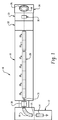
- Figure 1 is a schematic block diagram of a high-energy ion implanter into which is incorporated the present invention for reducing x-ray emissions;
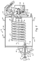
- Figure 2 shows a cross sectional view of one of a plurality of resonator modules that make up the linear accelerator portion of the ion implanter of Figure 1;
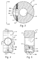
- Figure 3 is a more detailed, cross sectional view of the accelerating electrode of the resonator module of Figure 2;
- Figure 4 is a sectional view of the electrode of Figure 3 taken along the lines 4-4 of Figure 3; and
- Figure 5 is a sectional view of the electrode of Figure 3 taken along the lines 5-5 of Figure 4.
-
- A cross sectional plan view of a high-
energy ion implanter 10 is shown in Figure 1. Although the invention is described herein as being incorporated into an accelerating electrode in the RF linac portion of a high-energy ion implanter, it is understood that the invention may be incorporated into ion implanter components other than electrodes, and in ion implanter types other than high-energy. The invention is useful in any application wherein a reduction in x-ray emissions is desired, which would otherwise be generated by stray high-energy electrons striking structural components of the implanter. - The
implanter 10 comprises five sections or subsystems: aninjector 12 including anion source 14 for producing anion beam 15 and amass analysis magnet 16 for mass analyzing the ion beam; a radio frequency (RF) linear accelerator (linac) 18 including a plurality ofresonator modules 20a-20n for accelerating the ion beam to a higher energy; a final energy magnet (FEM) 22 for performing final mass analysis of the accelerated ion beam; a resolver housing 23 for final resolution and conditioning of the ion beam; and anend station 24 which contains a rotatingdisc 26 carrying wafers W to be implanted by the ion beam. - Positioned after the
mass analysis magnet 16 at the entrance to thelinac 18 is avariable aperture 30 for controlling the amount of beam current passing into the linac. Immediately downstream of theaperture 30 is a first flag Faraday 31 for measuring the beam current out of theaperture 30 and into thelinac 18. A second flag Faraday 35 is located in the resolver housing 23 for measuring the current of the ion beam prior to implanting into the wafer W. - The
mass analysis magnet 16 functions to pass to theRF linac 18 only the ions generated by theion source 14 having an appropriate charge-to-mass ratio. The mass analysis magnet is required because theion source 14, in addition to generating ions of appropriate charge-to-mass ratio, also generates ions of greater or lesser charge-to-mass ratio than that desired. Ions having inappropriate charge-to-mass ratios are not suitable for implantation into the wafer. - The ion beam that passes through the
mass analysis magnet 16 is typically comprised of a single isotope and enters theRF linac 18 which imparts additional energy to the ion beam passing therethrough. The RF linac produces particle accelerating fields which vary periodically with time, the phase of which may be adjusted to accommodate different atomic number particles as well as particles having different speeds. Each of the plurality ofresonator modules 20 in theRF linac 18 functions to further accelerate ions beyond the energies they achieve from a previous module. - Figure 2 shows a known type of
resonator module 20, comprising aninductor 62 formed by a coiled hollow copper tube. The high-voltage end of the coiled tube terminates in afirst coil stem 64 and the low-voltage end of the coiled tube terminates in asecond coil stem 66. Aspacer 67 snaps into place over the individual coil loops of theinductor 62 to maintain the distance between coil loops (and hence the inductance of the coil), and to provide mechanical stability for the inductor. The coil resides in acylindrical housing 68, in this case made of aluminum, which is electrically grounded during operation.Handles 69 are provided for removing and installing the resonator 60 from and into thesystem 10. - An RF input coupling (not visible in Figure 2) is provided to input an RF signal into the low-voltage end of the
inductor 62. A cylindrical high-voltage accelerating electrode ordrift tube 72 is attached to the high-voltage end of the inductor, atend 70 of thefirst coil stem 64. Thedrift tube 72 is fabricated of aluminum, and forms apassage 74 through which may pass an ion beam to be accelerated. - The resonator 60 is designed to resonate at the frequency of 13.56 megahertz (MHz). At resonance, a voltage greater than 20,000 volts (20 KV), and typically on the order of 80,000 volts (80 KV), is generated by the resonator at the
accelerator electrode 72. As such, a ceramic insulatingcone 80 extends from the grounded resonator housing toward the electrode to prevent arcing of between the housing and theelectrode 72 or the high-voltage coil stem 64. Anannular metal flange 82 is attached to the electrically grounded housing byfasteners 84 to secure the position of the insulatingcone 80. - The mechanism for tuning the resonator 60 is provided by a metallic
split ring clamp 88 located on the high-voltage stem 64 of the resonator coil, and aplunger 90 which is adapted to move in and out of the coil along its centrallongitudinal axis 92. Aservomotor 94 functions to bidirectionally move the plunger alongaxis 92. Apulley 96 on the servomotor shaft is connected to apulley 98 on theplunger shaft 100 viabelt 102. Threads on the inside of theplunger shaft pulley 98 mate with threads on the outside of theplunger shaft 100 to convert rotational motion of thepulley 98 to linear movement of theshaft 100 alongaxis 92. - The low-voltage, high-
current coil stem 66 and theplunger shaft 100 pass through a generally circular shapedaluminum end plate 104 which closes one end of the aluminumcylindrical housing 68. Because of the high current that passes through the coil at this end, heat is generated during operation of the resonator. As such, water-cooling means 106 are provided in the present invention for cooling theend plate 104, theplunger 90, and thecoil 62. - Figures 3 through 5 shows the accelerating
electrode 72 in greater detail. According the present invention, x-ray emissions, that would otherwise result from stray electrons striking the acceleratingelectrode 72, are minimized by coating the electrode with a synthetic diamond or diamond-like material. The type of electrode shown is merely one type of electrode used on resonator modules in RF linacs, and is merely shown as one example. In addition, it is contemplated that the synthetic diamond or diamond-like material may be used to coat other portions of an ion implanter exposed to the ion beam. - As shown in Figures 3-5, the
aluminum electrode 72 includes an RF coupling bore 108 for receivinghigh voltage end 70 of the firstcopper coil stem 64. Thebore 108 comprises ainner bore 108A for receiving and seating coil stemend 70 and anouter bore 108B for receiving and seating an RF connector atledge 110. The RF connector insures good electrical contact between the copper coil stemend 70 and thealuminum electrode 72. Asetscrew 112 screwed into threadedbore 113 secures the copper coil stemend 70 withinbore 108A. - A synthetic diamond or diamond-like coating (DLC) 114 is applied to the exposed exterior surface of the aluminum electrode 72 (but not the RF bore 108 or setscrew bore 113, which remain masked during the coating process). In the disclosed example, the diamond film has a thickness in the range of 2-10 microns (µm). The diamond or DLC is applied by known processes including chemical vapor deposition (CVD). The surface of the electrode may be roughened prior to the CVD process to facilitate adherence of the diamond or DLC to the electrode.
- The diamond or DLC has a high thermal conductivity, and is very stable chemically. As such, little or no diamond material is sputtered from the
electrode 72 during operation of thelinac 18 that would otherwise be transported along with theion beam 15. Thus, contamination problems that originate with the electrode are minimized. - In addition to the
aluminum electrode 72, other components in the ion implanter beamline that are exposed to vacuum conditions may be coated to minimize production of x-rays during implanter operation. For example, other electrodes that accelerate (or decelerate) the ion beam, or beamline or process chamber walls, may be coated with the diamond or DLC. All that is necessary is that there be an underlying base structure which is capable of being coated with a diamond or DLC layer. - The DLC, which is an amorphous (hydrogenated) carbon material comprising a random covalent network of graphitic-type structures, resemble the properties of diamond.
The carbon component of the diamond or DLC helps minimize the production of x-rays, due to the dependence of the Bremsstrahlung radiation-generating process on the atomic mass of the target material. The carbon-based diamond or DLC, having less atomic mass than the underlying aluminum electrode, produces less radiation as a target than does the uncoated aluminum electrode. Accordingly, less shielding is required in the implanter enclosure. - Although the invention has been described in terms of diamond, or DLC, it is contemplated that other, low atomic number (e.g., 6 or less) elements may be substituted. For example, coatings of lithium, beryllium or boron would also serve to minimize x-ray generation.
- Accordingly, a preferred embodiment of the use of diamond or diamond-like coated components in an ion implanter for reducing x-ray emissions has been described. With the foregoing description in mind, however, it is understood that this description is made only by way of example, that the invention is not limited to the particular embodiments described herein, and that various rearrangements, modifications, and substitutions may be implemented with respect to the foregoing description without departing from the scope of the invention as defined by the following claims and their equivalents.
Claims (18)
- A component of an ion implanter (10) for reducing x-ray emissions generated by the component when struck by electrons during operation of the implanter, comprising:a base structure (72) providing a coatable surface; anda coating (114) applied to said coatable surface of said base structure (72), said coating comprised of a material having as lesser atomic mass that that of the base structure, such that electrons impacting said coating produce less x-rays than electrons impacting said base structure.
- The component of claim 1, wherein said base structure is an electrode (72) through which an ion beam (15) passes during operation of the ion implanter (10).
- The component of claim 2, wherein said electrode is an accelerating electrode in a radio frequency (RF) linear accelerator (linac) (18).
- The component of claim 3, wherein said electrode carries a voltage of at least 20,000 volts (20 KV).
- The component of claim 4, wherein said electrode carries a voltage of approximately 80,000 volts (80 KV).
- The component of claim 3, wherein said coating is comprised of an element having an atomic number of less than six.
- The component of claim 3, wherein said coating (114) is a carbon-based material.
- The component of claim 7, wherein said coating (114) is a synthetic diamond or diamond-like coating (DLC) material.
- The component of claim 8, wherein said base structure (72) is comprised of aluminum.
- The component of claim 8, wherein said coating (114) has a thickness of approximately two to ten (2-10) microns (µm).
- The component of claim 10, wherein said coating (114) is applied to said base structure (72) by a chemical vapor deposition (CVD) process.
- A method of operating an ion implanter (10), comprising the steps of:generating an ion beam (15) with an ion source (14); andpassing the ion beam (15) through an accelerating electrode (72) in a radio frequency (RF) linear accelerator (linac) (18), said electrode comprising a coatable base structure and a coating (114) applied thereto, said coating comprised of a material having as lesser atomic mass that that of the base structure, such that electrons impacting said coating produce less x-rays than electrons impacting said base structure;
- The method of claim 12, wherein said electrode carries a voltage of at least 20,000 volts (20 KV).
- The method of claim 13, wherein said electrode carries a voltage of approximately 80,000 volts (80 KV).
- The method of claim 12, wherein said coating (114) is comprised of an element having an atomic number of less than six.
- The method of claim 12, wherein said coating (114) is a carbon-based material.
- The method of claim 16, wherein said coating (114) is a synthetic diamond or diamond-like coating (DLC) material.
- The method of claim 17, wherein said coating (114) has a thickness of approximately two to ten (2-10) microns (µm).
Applications Claiming Priority (2)
| Application Number | Priority Date | Filing Date | Title |
|---|---|---|---|
| US46036799A | 1999-12-13 | 1999-12-13 | |
| US460367 | 1999-12-13 |
Publications (1)
| Publication Number | Publication Date |
|---|---|
| EP1109196A1 true EP1109196A1 (en) | 2001-06-20 |
Family
ID=23828424
Family Applications (1)
| Application Number | Title | Priority Date | Filing Date |
|---|---|---|---|
| EP00310618A Withdrawn EP1109196A1 (en) | 1999-12-13 | 2000-11-30 | Diamond-like coated components in an ion implanter for reducing x-ray emissions |
Country Status (5)
| Country | Link |
|---|---|
| EP (1) | EP1109196A1 (en) |
| JP (1) | JP2001210266A (en) |
| KR (1) | KR20010061987A (en) |
| SG (1) | SG124233A1 (en) |
| TW (1) | TW490703B (en) |
Cited By (18)
| Publication number | Priority date | Publication date | Assignee | Title |
|---|---|---|---|---|
| US7134381B2 (en) | 2003-08-21 | 2006-11-14 | Nissan Motor Co., Ltd. | Refrigerant compressor and friction control process therefor |
| US7146956B2 (en) | 2003-08-08 | 2006-12-12 | Nissan Motor Co., Ltd. | Valve train for internal combustion engine |
| US7228786B2 (en) | 2003-06-06 | 2007-06-12 | Nissan Motor Co., Ltd. | Engine piston-pin sliding structure |
| US7255083B2 (en) | 2002-10-16 | 2007-08-14 | Nissan Motor Co., Ltd. | Sliding structure for automotive engine |
| US7273655B2 (en) | 1999-04-09 | 2007-09-25 | Shojiro Miyake | Slidably movable member and method of producing same |
| US7284525B2 (en) | 2003-08-13 | 2007-10-23 | Nissan Motor Co., Ltd. | Structure for connecting piston to crankshaft |
| US7318514B2 (en) | 2003-08-22 | 2008-01-15 | Nissan Motor Co., Ltd. | Low-friction sliding member in transmission, and transmission oil therefor |
| US7322749B2 (en) | 2002-11-06 | 2008-01-29 | Nissan Motor Co., Ltd. | Low-friction sliding mechanism |
| US7406940B2 (en) | 2003-05-23 | 2008-08-05 | Nissan Motor Co., Ltd. | Piston for internal combustion engine |
| US7458585B2 (en) | 2003-08-08 | 2008-12-02 | Nissan Motor Co., Ltd. | Sliding member and production process thereof |
| US7500472B2 (en) | 2003-04-15 | 2009-03-10 | Nissan Motor Co., Ltd. | Fuel injection valve |
| US7572200B2 (en) | 2003-08-13 | 2009-08-11 | Nissan Motor Co., Ltd. | Chain drive system |
| US7771821B2 (en) | 2003-08-21 | 2010-08-10 | Nissan Motor Co., Ltd. | Low-friction sliding member and low-friction sliding mechanism using same |
| GB2470287A (en) * | 2009-05-13 | 2010-11-17 | Micromass Ltd | Diamond like carbon coating on surface of a sampling cone of a mass spectrometer |
| US8096205B2 (en) | 2003-07-31 | 2012-01-17 | Nissan Motor Co., Ltd. | Gear |
| US8206035B2 (en) | 2003-08-06 | 2012-06-26 | Nissan Motor Co., Ltd. | Low-friction sliding mechanism, low-friction agent composition and method of friction reduction |
| US8471198B2 (en) | 2009-05-13 | 2013-06-25 | Micromass Uk Limited | Mass spectrometer sampling cone with coating |
| CN109075067A (en) * | 2016-06-28 | 2018-12-21 | 应用材料公司 | The diamond like carbon layer that electron beam plasma technique is formed |
Families Citing this family (7)
| Publication number | Priority date | Publication date | Assignee | Title |
|---|---|---|---|---|
| US7105840B2 (en) * | 2005-02-03 | 2006-09-12 | Axcelis Technologies, Inc. | Ion source for use in an ion implanter |
| CN103779162A (en) * | 2012-11-09 | 2014-05-07 | 北京中科信电子装备有限公司 | Ion implanter accelerator |
| JP6785188B2 (en) * | 2017-05-31 | 2020-11-18 | 住友重機械イオンテクノロジー株式会社 | Ion implantation device and ion implantation method |
| JP6785189B2 (en) * | 2017-05-31 | 2020-11-18 | 住友重機械イオンテクノロジー株式会社 | Ion implantation device and ion implantation method |
| US10342114B2 (en) * | 2017-09-15 | 2019-07-02 | Axcelis Technologies, Inc. | RF resonator for ion beam acceleration |
| TWI649775B (en) * | 2018-01-02 | 2019-02-01 | 台灣積體電路製造股份有限公司 | Ion implanter and method of manufacturing chamber of ion implanter |
| CN116417317B (en) * | 2021-12-30 | 2025-10-21 | 北京烁科中科信电子装备有限公司 | A structure for improving the acceleration efficiency of radio frequency acceleration barrel in ion implantation system |
Citations (4)
| Publication number | Priority date | Publication date | Assignee | Title |
|---|---|---|---|---|
| EP0375169A1 (en) * | 1988-11-24 | 1990-06-27 | The Agency of Industrial Science and Technology | External resonance circuit type radio frequency quadrupole acceleration |
| EP0648857A1 (en) * | 1993-08-27 | 1995-04-19 | Hughes Aircraft Company | Confinement of secondary electrons in plasma ion processing |
| US5916370A (en) * | 1998-06-12 | 1999-06-29 | Applied Materials, Inc. | Semiconductor processing chamber having diamond coated components |
| US5952060A (en) * | 1996-06-14 | 1999-09-14 | Applied Materials, Inc. | Use of carbon-based films in extending the lifetime of substrate processing system components |
-
2000
- 2000-11-21 TW TW089124623A patent/TW490703B/en not_active IP Right Cessation
- 2000-11-28 JP JP2000361124A patent/JP2001210266A/en active Pending
- 2000-11-28 SG SG200006871A patent/SG124233A1/en unknown
- 2000-11-29 KR KR1020000071526A patent/KR20010061987A/en not_active Ceased
- 2000-11-30 EP EP00310618A patent/EP1109196A1/en not_active Withdrawn
Patent Citations (4)
| Publication number | Priority date | Publication date | Assignee | Title |
|---|---|---|---|---|
| EP0375169A1 (en) * | 1988-11-24 | 1990-06-27 | The Agency of Industrial Science and Technology | External resonance circuit type radio frequency quadrupole acceleration |
| EP0648857A1 (en) * | 1993-08-27 | 1995-04-19 | Hughes Aircraft Company | Confinement of secondary electrons in plasma ion processing |
| US5952060A (en) * | 1996-06-14 | 1999-09-14 | Applied Materials, Inc. | Use of carbon-based films in extending the lifetime of substrate processing system components |
| US5916370A (en) * | 1998-06-12 | 1999-06-29 | Applied Materials, Inc. | Semiconductor processing chamber having diamond coated components |
Cited By (23)
| Publication number | Priority date | Publication date | Assignee | Title |
|---|---|---|---|---|
| US7273655B2 (en) | 1999-04-09 | 2007-09-25 | Shojiro Miyake | Slidably movable member and method of producing same |
| US7255083B2 (en) | 2002-10-16 | 2007-08-14 | Nissan Motor Co., Ltd. | Sliding structure for automotive engine |
| US7322749B2 (en) | 2002-11-06 | 2008-01-29 | Nissan Motor Co., Ltd. | Low-friction sliding mechanism |
| US8152377B2 (en) | 2002-11-06 | 2012-04-10 | Nissan Motor Co., Ltd. | Low-friction sliding mechanism |
| US7500472B2 (en) | 2003-04-15 | 2009-03-10 | Nissan Motor Co., Ltd. | Fuel injection valve |
| US7406940B2 (en) | 2003-05-23 | 2008-08-05 | Nissan Motor Co., Ltd. | Piston for internal combustion engine |
| US7228786B2 (en) | 2003-06-06 | 2007-06-12 | Nissan Motor Co., Ltd. | Engine piston-pin sliding structure |
| US8096205B2 (en) | 2003-07-31 | 2012-01-17 | Nissan Motor Co., Ltd. | Gear |
| US8206035B2 (en) | 2003-08-06 | 2012-06-26 | Nissan Motor Co., Ltd. | Low-friction sliding mechanism, low-friction agent composition and method of friction reduction |
| US7146956B2 (en) | 2003-08-08 | 2006-12-12 | Nissan Motor Co., Ltd. | Valve train for internal combustion engine |
| US7458585B2 (en) | 2003-08-08 | 2008-12-02 | Nissan Motor Co., Ltd. | Sliding member and production process thereof |
| US8575076B2 (en) | 2003-08-08 | 2013-11-05 | Nissan Motor Co., Ltd. | Sliding member and production process thereof |
| US7572200B2 (en) | 2003-08-13 | 2009-08-11 | Nissan Motor Co., Ltd. | Chain drive system |
| US7284525B2 (en) | 2003-08-13 | 2007-10-23 | Nissan Motor Co., Ltd. | Structure for connecting piston to crankshaft |
| US7771821B2 (en) | 2003-08-21 | 2010-08-10 | Nissan Motor Co., Ltd. | Low-friction sliding member and low-friction sliding mechanism using same |
| US7134381B2 (en) | 2003-08-21 | 2006-11-14 | Nissan Motor Co., Ltd. | Refrigerant compressor and friction control process therefor |
| US7650976B2 (en) | 2003-08-22 | 2010-01-26 | Nissan Motor Co., Ltd. | Low-friction sliding member in transmission, and transmission oil therefor |
| US7318514B2 (en) | 2003-08-22 | 2008-01-15 | Nissan Motor Co., Ltd. | Low-friction sliding member in transmission, and transmission oil therefor |
| GB2470287A (en) * | 2009-05-13 | 2010-11-17 | Micromass Ltd | Diamond like carbon coating on surface of a sampling cone of a mass spectrometer |
| US8471198B2 (en) | 2009-05-13 | 2013-06-25 | Micromass Uk Limited | Mass spectrometer sampling cone with coating |
| GB2470287B (en) * | 2009-05-13 | 2013-11-20 | Micromass Ltd | Surface coating on sampling cone of mass spectrometer |
| US8785843B2 (en) | 2009-05-13 | 2014-07-22 | Micromass Uk Limited | Mass spectrometer sampling cone with coating |
| CN109075067A (en) * | 2016-06-28 | 2018-12-21 | 应用材料公司 | The diamond like carbon layer that electron beam plasma technique is formed |
Also Published As
| Publication number | Publication date |
|---|---|
| KR20010061987A (en) | 2001-07-07 |
| TW490703B (en) | 2002-06-11 |
| SG124233A1 (en) | 2006-08-30 |
| JP2001210266A (en) | 2001-08-03 |
Similar Documents
| Publication | Publication Date | Title |
|---|---|---|
| KR20010061987A (en) | Diamond-like coated components in an ion implanter for reducing x-ray emissions | |
| JP5212760B2 (en) | Ion source for ion implanter and repeller therefor | |
| KR0158235B1 (en) | Ion implantation system | |
| US7176469B2 (en) | Negative ion source with external RF antenna | |
| JPH09129172A (en) | Self-cleaning ion beam neutralization device and method for cleaning contaminants adhering to the inner surface thereof | |
| JPH0265033A (en) | Ion beam source for radio frequency | |
| KR19980080200A (en) | Method for generating ionized metal plasma using electron beam and magnetic field | |
| WO2015191311A1 (en) | Ion implantation source with textured interior surfaces | |
| JPH11354508A (en) | Ion beam processing equipment | |
| EP0375169B1 (en) | External resonance circuit type radio frequency quadrupole acceleration | |
| CN101103432B (en) | Electron injection in ion implanter magnets | |
| US6291828B1 (en) | Glass-like insulator for electrically isolating electrodes from ion implanter housing | |
| EP0094473B1 (en) | Apparatus and method for producing a stream of ions | |
| JP3896543B2 (en) | A mechanism for suppressing neutron radiation in the beam line of an ion implanter. | |
| US6071595A (en) | Substrate with low secondary emissions | |
| EP0995214B1 (en) | Method and apparatus for neutralising space charge in an ion beam | |
| JP3064214B2 (en) | Fast atom beam source | |
| RU2796652C1 (en) | Device for forming a beam of cluster or atomic ions of gas | |
| JPH08241687A (en) | Ecr type ion source | |
| EP0095879B1 (en) | Apparatus and method for working surfaces with a low energy high intensity ion beam | |
| Dudnikov et al. | Direct current surface plasma source with high emission current density | |
| Dudnikov et al. | High current density negative ion source for beam line transport studies | |
| Fischer et al. | Construction of a simple low-energy high-intensity gas ion source with a multiaperture extractor system | |
| Chang | Ultra low energy gold cluster ion beams for SIMS applications | |
| Okada et al. | Characteristics of Hall accelerator for helium-ion beam extraction |
Legal Events
| Date | Code | Title | Description |
|---|---|---|---|
| PUAI | Public reference made under article 153(3) epc to a published international application that has entered the european phase |
Free format text: ORIGINAL CODE: 0009012 |
|
| AK | Designated contracting states |
Kind code of ref document: A1 Designated state(s): DE FR GB IT NL |
|
| AX | Request for extension of the european patent |
Free format text: AL;LT;LV;MK;RO;SI |
|
| 17P | Request for examination filed |
Effective date: 20010724 |
|
| AKX | Designation fees paid |
Free format text: DE FR GB IT NL |
|
| 17Q | First examination report despatched |
Effective date: 20040212 |
|
| STAA | Information on the status of an ep patent application or granted ep patent |
Free format text: STATUS: THE APPLICATION IS DEEMED TO BE WITHDRAWN |
|
| 18D | Application deemed to be withdrawn |
Effective date: 20040623 |