EP1107529A2 - Compensation of DC offsets on a DC-blocking channel - Google Patents
Compensation of DC offsets on a DC-blocking channel Download PDFInfo
- Publication number
- EP1107529A2 EP1107529A2 EP00310974A EP00310974A EP1107529A2 EP 1107529 A2 EP1107529 A2 EP 1107529A2 EP 00310974 A EP00310974 A EP 00310974A EP 00310974 A EP00310974 A EP 00310974A EP 1107529 A2 EP1107529 A2 EP 1107529A2
- Authority
- EP
- European Patent Office
- Prior art keywords
- offset
- recited
- modem
- compensating signal
- codec
- Prior art date
- Legal status (The legal status is an assumption and is not a legal conclusion. Google has not performed a legal analysis and makes no representation as to the accuracy of the status listed.)
- Granted
Links
Images

Classifications
-
- H—ELECTRICITY
- H04—ELECTRIC COMMUNICATION TECHNIQUE
- H04L—TRANSMISSION OF DIGITAL INFORMATION, e.g. TELEGRAPHIC COMMUNICATION
- H04L25/00—Baseband systems
- H04L25/02—Details ; arrangements for supplying electrical power along data transmission lines
- H04L25/06—DC level restoring means; Bias distortion correction ; Decision circuits providing symbol by symbol detection
- H04L25/061—DC level restoring means; Bias distortion correction ; Decision circuits providing symbol by symbol detection providing hard decisions only; arrangements for tracking or suppressing unwanted low frequency components, e.g. removal of DC offset
-
- H—ELECTRICITY
- H03—ELECTRONIC CIRCUITRY
- H03M—CODING; DECODING; CODE CONVERSION IN GENERAL
- H03M13/00—Coding, decoding or code conversion, for error detection or error correction; Coding theory basic assumptions; Coding bounds; Error probability evaluation methods; Channel models; Simulation or testing of codes
Definitions
- the present invention is directed, in general, to coder/decoders (codecs) and, more specifically, to a system and method for compensating for codec DC offset through a DC blocking channel and a modem incorporating the same.
- codecs coder/decoders
- 56K modems are currently the most popular means by which users can gain access to the Internet.
- 56K modems offer users asymmetric connection speeds. For data downloaded from the Internet to the user's modem, a connection speed of over 50 thousand bits per second (kbps) is possible.
- kbps bits per second
- the transmission path, or channel, connecting the modem to the codec contains a DC blocking device.
- the DC blocking device which usually takes the form of a transformer would serve to block any DC component before it could reach the codec and compensate for DC offset.
- the present invention provides a system for, and method of, compensating for codec DC offset and a modem incorporating the system or the method.
- the system includes: (1) a DC offset compensator that develops and transmits a DC offset indicator signal corresponding to a DC offset present along a transmission path to a receiving codec and (2) a DC offset encoder, coupled to the DC offset compensator, that receives the DC offset indicator signal and applies a time-varying DC offset compensating signal based thereon to a user data symbol stream transmitted along the transmission path.
- the DC offset compensator can employ the DC offset compensating signal to remove at least a portion of the DC offset compensating signal to yield the user data symbol stream.
- the present invention therefore introduces the broad concept of encoding compensation for codec DC offset in a deterministic, time-varying signal that is transmitted along with a user data symbol stream.
- the DC offset is, in effect, encoded into AC form.
- the time-varying signal can traverse any DC blocking circuitry, such as a transformer, and thereby reach the receiving codec. Because the time-varying signal is deterministic, circuitry proximate the receiving codec can compute and remove the time-varying signal, leaving the user data symbol stream for digitization.
- the DC offset compensating signal comprises a deterministic pseudo-random number sequence.
- Those skilled in the pertinent art are familiar with pseudo-random numbers and techniques for generating them.
- the present invention can make use of such techniques to generate the same pseudo-random number sequence at both the transmitting and receiving ends of a communications channel.
- the pseudo-random number sequence is first added to, and then subtracted from, a user data symbol stream to compensate for DC offset that may occur due to patterns in the user data symbol stream.
- the DC offset compensating signal has a component that tends to average about an oppositely signed negative of the DC offset.
- the component of the DC offset compensating signal tends to average about -C.
- the DC offset compensator removes an entirety of the DC offset compensating signal. This maximizes compensation for DC offset. However, in some embodiments of the present invention, some portion of the DC offset compensating signal may, or may be allowed to, remain. In the broad scope of the present invention, at least some DC offset compensation occurs.
- the DC offset compensator removes at least the portion of the DC offset compensating signal by recalculating the pseudo-random number sequence. Recalculation allows the pseudo-random number sequence to be at least partially removed from any user data symbol stream.
- the DC offset compensating signal is capable of passing substantially undistorted through a DC blocking transformer.
- the DC offset indicator signal may be somewhat distorted (or attenuated), but DC offset compensation still at least partially takes place by virtue of its presence.
- the DC offset encoder is associated with a 56K modem Those skilled in the pertinent art will appreciate that compensation for any DC offset that may occur at the receiving codec allows for higher upstream communication rates with such modems. Those skilled in the pertinent art will also understand that the principles of the present invention may be broadly applied in a variety of circumstances in which a DC signal is required to be encoded into AC form for the purpose of traversing a DC blocking circuit.
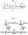
- FIGURE 1 illustrated is a block diagram of a portion of a telecommunications network, generally designated 100, that illustrates the problem addressed by the present invention.
- the network 100 includes a pulse-code modulating (PCM) codec 110 that provides analog-to-digital conversion between a local loop 120 and the network 100.
- PCM pulse-code modulating
- a 56k modem 130 is coupled to the local loop 120 distal from the codec 110.
- a DC blocking transformer 140 is coupled to the local loop 120 between the codec 110 and the modem 130. The DC blocking transformer 140 transforms the local loop 120 into a DC blocking channel.
- the upload speed of the modem 130 is limited by, among other things, DC offset occurring at the analog input of the codec 110.
- the present invention is directed to attenuating the DC offset, taking into account that the DC blocking transformer 140 blocks any DC signal that could be conventionally employed to compensate for DC offset at the analog input of the codec 110.
- FIGURE 2 illustrated is a block diagram of a system for compensating for codec DC offset constructed according to the principles of the present invention.
- the system comprises a DC offset compensator 210 (associated, in the illustrated embodiment, with a receiving codec, such as the codec 110 of FIGURE 1) and a DC offset encoder 220 (associated, in the illustrated embodiment, with a transmitting modem, such as the modem 130 of FIGURE 1).
- the DC offset compensator 210 detects the magnitude of DC offset occurring at the analog input of the receiving codec.
- the DC offset compensator 210 transmits a corresponding DC offset indicator signal 230 to the DC offset encoder 220, perhaps via a downloaded symbol stream.
- the DC offset encoder 220 In response, the DC offset encoder 220 generates a time-varying DC offset compensating signal 250 based on the DC offset indicator signal. It is important that the DC offset compensating signal 250 be time-varying, since the DC offset compensating signal 250 must later at least partially traverse a DC blocking transformer.
- DC offset compensating signal 250 be time-varying, since the DC offset compensating signal 250 must later at least partially traverse a DC blocking transformer.
- the DC offset compensating signal 250 has two components, a DC component and an AC component.
- the DC component is equal in magnitude and opposite in sign to the DC offset. For example, if the DC offset at a given point in time has a magnitude c, the DC component of the DC offset compensating signal has a corresponding magnitude -c.
- the AC component tk of the DC offset compensating signal 250 is a deterministic pseudo-random number sequence dynamically generated to average out to c.
- the RDS ⁇ k is defined as being equal to ⁇ S k .
- the DC offset encoder 220 causes the signal 250 to be applied (added) to a user data symbol stream 240.
- the user data symbol stream 240 is then transmitted from the modem along the local loop to the receiving codec.
- the user data symbol stream 240 encounters the DC blocking transformer 140 (represented in FIGURE 2 as a block rather than as a schematic symbol as it was in FIGURE 1).
- the DC blocking transformer 140 at least substantially removes the DC component, and allows the AC component and the user data symbol stream 240 to pass. Because the user data symbol stream 240 (including the remaining AC component of the DC offset compensating signal 250) averages out to 0 volts, DC bias has been reduced, and perhaps substantially eliminated, when the user data symbol stream reaches the input of the codec.
- the codec then converts the user data symbol stream to digital form. At this point, it is necessary to remove the converted AC component of the DC offset compensating signal from the user data. This is done by recalculating the AC component and subtracting it from the user data. Since, in the exemplary embodiment, the AC component is a deterministic pseudo-random number sequence, the DC offset compensator 210 can accurately recalculate the AC component. Once recalculated, the AC component can be subtracted from the user data, restoring the user data to useful form.
- FIGURE 3 illustrated is a method of compensating for codec DC offset carried out according to the principles of the present invention.
- the method begins in a start step 305, wherein it is desired to upload user data from a modem (perhaps to another modem, not shown) through a codec that is part of a telecommunications network.
- the method 300 continues in a step 310, wherein DC offset is detected at the input of the receiving codec. It being desirable at least to reduce this DC offset, a DC offset indicator signal is developed in a step 315 and transmitted to circuitry associated with the modem in a step 320.
- a time-varying DC offset compensating signal is generated based on the DC offset indicator signal (perhaps in the manner set forth above, but perhaps in any other appropriate manner).
- the DC offset compensating signal is then applied to a user data symbol stream to be transmitted from the modem to the codec in a step 330.
- the user data symbol stream (including the DC offset compensating signal) is transmitted to the input of the codec.
- the user data symbol stream encounters, and traverses, a DC blocking transformer.
- the user data symbol stream arrives at the codec and, because its average voltage is at or near zero, DC offset at the codec input has at least been reduced.
- the codec then digitizes the user data symbol stream to yield digitized user data in a step 340.
- circuitry associated with the codec recalculates the DC offset compensating signal in a step 345 and subtracts the DC offset compensating signal from the user data in a step 350. This yields user data in useful form for continued transmission to the telecommunications network.
- the method 300 then ends in an end step 355, at which point the user data are forwarded through the telecommunications network.
- FIGURE 4 illustrated is a block diagram of a 56k modem that incorporates the system of FIGURE 2 or the method of FIGURE 3.
- the 56k modem generally designated 400, comprises symbol stream generating circuitry 410.
- symbol stream generating circuitry 410 Those skilled in the art are familiar with the structure and function of symbol stream generating circuitry.
- the 56k modem 400 of the present invention advantageously employs such circuitry 410 for generating a user data symbol stream for uploading user data to a receiving codec (not shown in FIGURE 4).
- the 56k modem 400 further comprises a DC offset indicator signal receiver 420 responsible for receiving a DC offset indicator signal from circuitry associated with the receiving codec.
- the DC offset indicator indicates DC offset that exists along the transmission path joining the 56k modem 400 and the receiving codec.
- the 56k modem 400 further comprises a DC offset encoder 430 responsible for receiving the DC offset indicator signal from the DC offset indicator signal receiver 420 and developing therefrom a time-varying DC offset compensating signal that can be applied to the user data symbol stream produced by the symbol stream generating circuitry 410 to achieve DC offset compensation at the receiving codec in spite of any DC blocking circuitry present in the local loop that couples the modem 400 and the receiving codec.
- a DC offset encoder 430 responsible for receiving the DC offset indicator signal from the DC offset indicator signal receiver 420 and developing therefrom a time-varying DC offset compensating signal that can be applied to the user data symbol stream produced by the symbol stream generating circuitry 410 to achieve DC offset compensation at the receiving codec in spite of any DC blocking circuitry present in the local loop that couples the modem 400 and the receiving codec.
Landscapes
- Engineering & Computer Science (AREA)
- Power Engineering (AREA)
- Computer Networks & Wireless Communication (AREA)
- Signal Processing (AREA)
- Physics & Mathematics (AREA)
- Probability & Statistics with Applications (AREA)
- Theoretical Computer Science (AREA)
- Dc Digital Transmission (AREA)
- Amplifiers (AREA)
- Digital Transmission Methods That Use Modulated Carrier Waves (AREA)
Abstract
Description
if □k / c □ 0 then tk+1 = 0
else
tk = yk - xk, where yk is a PCM encoder level uniquely specified by the conditions:
□tk□ > □c□,
□tk□ is as small as possible, and
tk/c>0.
Claims (21)
- A system for compensating for codec DC offset, comprising:a DC offset compensator that develops and transmits a DC offset indicator signal corresponding to a DC offset present along a transmission path to a receiving codec; anda DC offset encoder, coupled to said DC offset compensator, that receives said DC offset indicator signal and applies a time-varying DC offset compensating signal based thereon to a user data symbol stream transmitted along said transmission path.
- The system as recited in Claim 1 wherein said DC offset compensating signal comprises a deterministic pseudo-random number sequence.
- The system as recited in Claim 1 wherein said DC offset compensating signal has a component that tends to average about an oppositely signed negative of said DC offset.
- The system as recited in Claim 1 wherein said DC offset compensator removes an entirety of said DC offset.
- The system as recited in Claim 1 wherein said DC offset compensator recalculates said DC offset compensating signal.
- The system as recited in Claim 1 wherein said DC offset compensating signal is capable of passing substantially undistorted through a DC blocking transformer.
- The system as recited in Claim 1 wherein said DC offset encoder is associated with a 56K modem.
- A method of compensating for codec DC offset, comprising:developing a DC offset indicator signal corresponding to a DC offset present along a transmission path to a receiving codec;applying a time-varying DC offset compensating signal, based on said DC offset indicator signal, to a user data symbol stream transmitted along said transmission path; andremoving at least a portion of said DC offset compensating signal to substantially yield said symbol stream.
- The method as recited in Claim 8 wherein said removing is performed proximate said receiving codec.
- The method as recited in Claim 8 wherein said DC offset compensating signal comprises a deterministic pseudo-random number sequence.
- The method as recited in Claim 8 wherein said DC offset compensating signal has a component that tends to average about an oppositely signed negative of said DC offset.
- The method as recited in Claim 8 wherein said removing comprises removing an entirety of said DC offset compensating signal.
- The method as recited in Claim 8 wherein said removing comprises recalculating said DC offset compensating signal.
- The method as recited in Claim 8 wherein said DC offset compensating signal is capable of passing substantially undistorted through a DC blocking transformer.
- The method as recited in Claim 8 wherein said DC offset encoder is associated with a 56K modem
- A modem, comprising:a DC offset indicator signal receiver that receives a DC offset indicator signal corresponding to a DC offset present along a transmission path to a receiving codec coupled to said modem;symbol stream generating circuitry that generates a user data symbol stream containing user data; anda DC offset encoder, coupled to said DC offset compensator, that applies a time-varying DC offset compensating signal based thereon to a user data symbol stream transmitted along said transmission path.
- The modem as recited in Claim 16 wherein said DC offset compensating signal comprises a deterministic pseudo-random number sequence.
- The modem as recited in Claim 16 wherein said DC offset compensating signal has a component that tends to average about an oppositely signed negative of said DC offset.
- The modem as recited in Claim 16 wherein said DC offset compensating signal is capable of passing substantially undistorted through a DC blocking transformer.
- The modem as recited in Claim 16 wherein said DC offset indicator signal changes throughout a given modem session.
- The modem as recited in Claim 16 wherein said modem is a 56K modem.
Applications Claiming Priority (4)
| Application Number | Priority Date | Filing Date | Title |
|---|---|---|---|
| US16996199P | 1999-12-09 | 1999-12-09 | |
| US169961P | 1999-12-09 | ||
| US695671 | 2000-10-24 | ||
| US09/695,671 US6496124B1 (en) | 1999-12-09 | 2000-10-24 | System and method for compensating for codec DC offset through a DC blocking channel and modem incorporating the same |
Publications (3)
| Publication Number | Publication Date |
|---|---|
| EP1107529A2 true EP1107529A2 (en) | 2001-06-13 |
| EP1107529A3 EP1107529A3 (en) | 2004-06-09 |
| EP1107529B1 EP1107529B1 (en) | 2009-03-11 |
Family
ID=26865540
Family Applications (1)
| Application Number | Title | Priority Date | Filing Date |
|---|---|---|---|
| EP00310974A Expired - Lifetime EP1107529B1 (en) | 1999-12-09 | 2000-12-08 | Compensation of DC offsets on a DC-blocking channel |
Country Status (6)
| Country | Link |
|---|---|
| US (1) | US6496124B1 (en) |
| EP (1) | EP1107529B1 (en) |
| KR (1) | KR100755291B1 (en) |
| CA (1) | CA2327725C (en) |
| DE (1) | DE60041750D1 (en) |
| TW (1) | TW506202B (en) |
Families Citing this family (3)
| Publication number | Priority date | Publication date | Assignee | Title |
|---|---|---|---|---|
| EP1529357A4 (en) | 2002-05-13 | 2010-04-07 | Interdigital Tech Corp | ALLOCATION OF RESOURCES TO USERS IN TIME DIVISION MULTIPLE ACCESS CDMA (CDMA) SYSTEMS WHOSE OPERATION IS PERFORMED BY BEAMS |
| US8659456B2 (en) * | 2011-11-16 | 2014-02-25 | Mediatek Inc. | Electronic device and transmitter DC offset calibration method thereof |
| KR102664046B1 (en) | 2021-11-25 | 2024-05-08 | 광동제약 주식회사 | Methods on mass production of Ginseng and Ginseng clones through Hydroponic system |
Family Cites Families (4)
| Publication number | Priority date | Publication date | Assignee | Title |
|---|---|---|---|---|
| US5943365A (en) * | 1996-10-16 | 1999-08-24 | Cirrus Logic, Inc. | Device, system, and method for modem communication utilizing DC or near-DC signal suppression |
| US6278744B1 (en) * | 1996-11-15 | 2001-08-21 | Conexant Systems, Inc. | System for controlling and shaping the spectrum and redundancy of signal-point limited transmission |
| US6289070B1 (en) * | 1997-04-22 | 2001-09-11 | Silicon Laboratories, Inc. | Digital isolation system with ADC offset calibration including coarse offset |
| US5999109A (en) * | 1997-06-09 | 1999-12-07 | 3Com Corporation | Frame-based spectral shaping method and apparatus |
-
2000
- 2000-10-24 US US09/695,671 patent/US6496124B1/en not_active Expired - Lifetime
- 2000-12-05 TW TW089125909A patent/TW506202B/en not_active IP Right Cessation
- 2000-12-06 CA CA002327725A patent/CA2327725C/en not_active Expired - Fee Related
- 2000-12-08 DE DE60041750T patent/DE60041750D1/en not_active Expired - Lifetime
- 2000-12-08 EP EP00310974A patent/EP1107529B1/en not_active Expired - Lifetime
- 2000-12-08 KR KR1020000074506A patent/KR100755291B1/en not_active Expired - Fee Related
Also Published As
| Publication number | Publication date |
|---|---|
| US6496124B1 (en) | 2002-12-17 |
| EP1107529B1 (en) | 2009-03-11 |
| CA2327725A1 (en) | 2001-06-09 |
| TW506202B (en) | 2002-10-11 |
| DE60041750D1 (en) | 2009-04-23 |
| CA2327725C (en) | 2005-06-21 |
| KR20010062245A (en) | 2001-07-07 |
| EP1107529A3 (en) | 2004-06-09 |
| KR100755291B1 (en) | 2007-09-05 |
Similar Documents
| Publication | Publication Date | Title |
|---|---|---|
| EP0929958B1 (en) | Rob bit compensation system and method associated with a receiver or codec | |
| KR0131815B1 (en) | Digital data over voice communication | |
| US7933341B2 (en) | System and method for high speed communications using digital signal processing | |
| US6393029B1 (en) | Use of modified line encoding and low signal-to-noise auto ratio based signal processing to extend range of digital data transmission over repeaterless two-wire telephone link | |
| US6505222B1 (en) | Systems methods and computer program products for controlling undesirable bias in an equalizer | |
| JP4160097B2 (en) | High speed communication system for analog subscriber connection. | |
| JPH0211057A (en) | Data communication method and communication network | |
| US6421320B1 (en) | Asymmetric modem communications system and method | |
| FI104134B (en) | Data and power supply realizing cable adaptation | |
| US6034993A (en) | Method and apparatus for adaptively equalizing a signal received from a remote transmitter | |
| US6965578B1 (en) | Echo canceling method and apparatus for digital data communication system | |
| WO2001065788A9 (en) | System and method for high speed communications using digital signal processing | |
| US20110261863A1 (en) | Reducing Transmit Signal Components of a Receive Signal of a Transceiver | |
| US6496124B1 (en) | System and method for compensating for codec DC offset through a DC blocking channel and modem incorporating the same | |
| US6804291B1 (en) | Device and method of digital gain programming using sigma-delta modulator | |
| US6504865B1 (en) | Digital connection detection technique | |
| JP3701840B2 (en) | How to detect and compensate for telephone network degradation | |
| JP3662843B2 (en) | System and method for compensating for codec DC offset using a DC blocking channel and modem incorporating the same | |
| US6901107B1 (en) | Systems, methods, and computer program products for generating a digital impairment learning signal having low energy content at direct current and Nyquist frequencies | |
| US7272174B2 (en) | Upstream data transmission | |
| US7593479B2 (en) | Precoding for a non-linear codec | |
| US7099403B1 (en) | Precoding for a non-linear codec | |
| JP4888753B2 (en) | Precoding for nonlinear codecs | |
| US7123661B2 (en) | Datastream transmitters for discrete multitone systems | |
| Vry | Digital local network systems: The impact of signal processing |
Legal Events
| Date | Code | Title | Description |
|---|---|---|---|
| PUAI | Public reference made under article 153(3) epc to a published international application that has entered the european phase |
Free format text: ORIGINAL CODE: 0009012 |
|
| AK | Designated contracting states |
Kind code of ref document: A2 Designated state(s): AT BE CH CY DE DK ES FI FR GB GR IE IT LI LU MC NL PT SE TR |
|
| AX | Request for extension of the european patent |
Free format text: AL;LT;LV;MK;RO;SI |
|
| PUAL | Search report despatched |
Free format text: ORIGINAL CODE: 0009013 |
|
| RIC1 | Information provided on ipc code assigned before grant |
Ipc: 7H 04L 27/36 B Ipc: 7H 04L 25/06 A Ipc: 7H 04L 25/03 B Ipc: 7H 04B 1/62 B Ipc: 7H 04L 25/49 B |
|
| AK | Designated contracting states |
Kind code of ref document: A3 Designated state(s): AT BE CH CY DE DK ES FI FR GB GR IE IT LI LU MC NL PT SE TR |
|
| AX | Request for extension of the european patent |
Extension state: AL LT LV MK RO SI |
|
| 17P | Request for examination filed |
Effective date: 20041011 |
|
| 17Q | First examination report despatched |
Effective date: 20041215 |
|
| AKX | Designation fees paid |
Designated state(s): DE FR GB |
|
| GRAP | Despatch of communication of intention to grant a patent |
Free format text: ORIGINAL CODE: EPIDOSNIGR1 |
|
| GRAS | Grant fee paid |
Free format text: ORIGINAL CODE: EPIDOSNIGR3 |
|
| GRAJ | Information related to disapproval of communication of intention to grant by the applicant or resumption of examination proceedings by the epo deleted |
Free format text: ORIGINAL CODE: EPIDOSDIGR1 |
|
| GRAP | Despatch of communication of intention to grant a patent |
Free format text: ORIGINAL CODE: EPIDOSNIGR1 |
|
| GRAS | Grant fee paid |
Free format text: ORIGINAL CODE: EPIDOSNIGR3 |
|
| GRAA | (expected) grant |
Free format text: ORIGINAL CODE: 0009210 |
|
| AK | Designated contracting states |
Kind code of ref document: B1 Designated state(s): DE FR GB |
|
| REG | Reference to a national code |
Ref country code: GB Ref legal event code: FG4D |
|
| REF | Corresponds to: |
Ref document number: 60041750 Country of ref document: DE Date of ref document: 20090423 Kind code of ref document: P |
|
| RAP4 | Party data changed (patent owner data changed or rights of a patent transferred) |
Owner name: LUCENT TECHNOLOGIES INC. |
|
| PLBE | No opposition filed within time limit |
Free format text: ORIGINAL CODE: 0009261 |
|
| STAA | Information on the status of an ep patent application or granted ep patent |
Free format text: STATUS: NO OPPOSITION FILED WITHIN TIME LIMIT |
|
| 26N | No opposition filed |
Effective date: 20091214 |
|
| PGFP | Annual fee paid to national office [announced via postgrant information from national office to epo] |
Ref country code: GB Payment date: 20131204 Year of fee payment: 14 Ref country code: DE Payment date: 20131204 Year of fee payment: 14 |
|
| PGFP | Annual fee paid to national office [announced via postgrant information from national office to epo] |
Ref country code: FR Payment date: 20131209 Year of fee payment: 14 |
|
| REG | Reference to a national code |
Ref country code: DE Ref legal event code: R119 Ref document number: 60041750 Country of ref document: DE |
|
| GBPC | Gb: european patent ceased through non-payment of renewal fee |
Effective date: 20141208 |
|
| REG | Reference to a national code |
Ref country code: FR Ref legal event code: ST Effective date: 20150831 |
|
| PG25 | Lapsed in a contracting state [announced via postgrant information from national office to epo] |
Ref country code: GB Free format text: LAPSE BECAUSE OF NON-PAYMENT OF DUE FEES Effective date: 20141208 Ref country code: DE Free format text: LAPSE BECAUSE OF NON-PAYMENT OF DUE FEES Effective date: 20150701 |
|
| PG25 | Lapsed in a contracting state [announced via postgrant information from national office to epo] |
Ref country code: FR Free format text: LAPSE BECAUSE OF NON-PAYMENT OF DUE FEES Effective date: 20141231 |