EP1107459A2 - Method and apparatus for digitally removing a DC-offset smaller than one LSB - Google Patents
Method and apparatus for digitally removing a DC-offset smaller than one LSB Download PDFInfo
- Publication number
- EP1107459A2 EP1107459A2 EP00310487A EP00310487A EP1107459A2 EP 1107459 A2 EP1107459 A2 EP 1107459A2 EP 00310487 A EP00310487 A EP 00310487A EP 00310487 A EP00310487 A EP 00310487A EP 1107459 A2 EP1107459 A2 EP 1107459A2
- Authority
- EP
- European Patent Office
- Prior art keywords
- bit
- signal path
- input
- offset
- filter
- Prior art date
- Legal status (The legal status is an assumption and is not a legal conclusion. Google has not performed a legal analysis and makes no representation as to the accuracy of the status listed.)
- Granted
Links
- 238000000034 method Methods 0.000 title claims description 9
- 230000004044 response Effects 0.000 claims abstract description 14
- 238000001914 filtration Methods 0.000 claims description 9
- 238000010586 diagram Methods 0.000 description 11
- 230000010354 integration Effects 0.000 description 6
- 238000006243 chemical reaction Methods 0.000 description 3
- 230000006870 function Effects 0.000 description 3
- 230000001413 cellular effect Effects 0.000 description 2
- 230000001627 detrimental effect Effects 0.000 description 2
- 238000010276 construction Methods 0.000 description 1
- 230000003247 decreasing effect Effects 0.000 description 1
- 230000009467 reduction Effects 0.000 description 1
Images


Classifications
-
- H—ELECTRICITY
- H03—ELECTRONIC CIRCUITRY
- H03M—CODING; DECODING; CODE CONVERSION IN GENERAL
- H03M1/00—Analogue/digital conversion; Digital/analogue conversion
- H03M1/06—Continuously compensating for, or preventing, undesired influence of physical parameters
- H03M1/0617—Continuously compensating for, or preventing, undesired influence of physical parameters characterised by the use of methods or means not specific to a particular type of detrimental influence
- H03M1/0626—Continuously compensating for, or preventing, undesired influence of physical parameters characterised by the use of methods or means not specific to a particular type of detrimental influence by filtering
-
- H—ELECTRICITY
- H03—ELECTRONIC CIRCUITRY
- H03M—CODING; DECODING; CODE CONVERSION IN GENERAL
- H03M1/00—Analogue/digital conversion; Digital/analogue conversion
- H03M1/06—Continuously compensating for, or preventing, undesired influence of physical parameters
- H03M1/0602—Continuously compensating for, or preventing, undesired influence of physical parameters of deviations from the desired transfer characteristic
- H03M1/0604—Continuously compensating for, or preventing, undesired influence of physical parameters of deviations from the desired transfer characteristic at one point, i.e. by adjusting a single reference value, e.g. bias or gain error
- H03M1/0607—Offset or drift compensation
-
- H—ELECTRICITY
- H03—ELECTRONIC CIRCUITRY
- H03M—CODING; DECODING; CODE CONVERSION IN GENERAL
- H03M1/00—Analogue/digital conversion; Digital/analogue conversion
- H03M1/12—Analogue/digital converters
Definitions
- This invention relates generally to radio telephones and personal communicators, referred to herein generally as mobile stations, and more particularly to radio frequency (RF) receivers for these and other devices that are subject to direct current (DC) offset signals.
- RF radio frequency
- ADC analog to digital converter
- DSP digital signal processor
- FIR Finite Impulse Response
- the magnitude of the DC offset corresponding to 1/2 LSB will become larger.
- a one volt signal is expressed in an eight bit format
- a step size of the 256 possible digital values will represent about 4 millivolts, and one half of the LSB will then be about 2 millivolts.
- a step size of the 64 possible digital values will represent about 15.5 millivolts, and one half of the LSB will be about 7.7 millivolts.
- One way to reduce the magnitude of the DC offset is to specify a more expensive ADC having more bits of resolution and/or a tighter tolerance for the DC offset output from the ADC.
- this adds cost to the device containing the ADC.
- the required ADC may require a longer conversion time, and may as well have a larger power consumption, which is detrimental in battery-powered equipment.
- the overall cost can be essentially doubled.
- a signal path such as receiver signal path of a mobile station, includes an analog to digital converter (ADC) for representing an input signal as n-bits, the n-bit representation including a DC offset component.
- the signal path may be one of an Inphase (I) or a Quadrature (Q) signal path of the mobile station.
- the summing node operates to subtract the value appearing at the second input from the value appearing at the first input, and outputs a k-bit DC offset compensated value.
- a filter such as a finite impulse response (FIR) filter or an infinite impulse response (IIR) filter, is coupled to the output of the summing node.
- a negative feedback path is provided from an output of the filter to the second input of the summing node for generating the k-bit representation of the DC offset component compensation value.
- the signal path includes the ADC for representing the input signal as n-bits, the n-bit representation comprising a DC offset component.
- the summing node in this embodiment has the first input coupled to the filter output for inputting the k-bit output of the filter and the second input inputs the k-bit representation of the DC offset component compensation value. The summing node operates to subtract the value appearing at said second input from the value appearing at said first input, and outputs the k-bit DC offset compensated value.
- the mobile station 10 may be a radiotelephone, such as a cellular telephone or a personal communicator.
- the mobile station 10 includes a micro-control unit (MCU) 12 having an output coupled to an input of a display 14 and an input coupled to an output of a keyboard or keypad 16.
- the keypad 16 enables characters to be entered for display on display 14, as well as mobile station 10 control functions to be exercised.
- the MCU 12 is assumed to include or be coupled to some type of a read-only memory (ROM) 12A for storing an operating program, as well as a random access memory (RAM) 12B for temporarily storing inputted characters from the keypad 16 or the receiver 22, as well as other required data, scratchpad memory, etc.
- ROM read-only memory
- RAM random access memory
- the mobile station 10 has a wireless or radio section that includes a digital signal processor (DSP) 18, or equivalent high speed processor, as well as a wireless transceiver comprised of a transmitter 20 and a receiver 22, both of which are coupled to an antenna 24.
- DSP digital signal processor
- An output of the receiver 22 is coupled to an ADC block 19 (actually two ADCs) which provides I and Q digital outputs to the DSP 18.
- the DSP 18 may implement a FIR filter block 18A (actually two FIR filters, one for the I channel and one for the Q channel), as well as other desired signal processing blocks (not shown) .
- the FIR filters 18A could be separate, external digital processing blocks that feed their outputs into the DSP 18.
- Fig. 2A is a waveform diagram depicting a representative analog input signal of the ADC 19 and the corresponding digital output signal, as well as the undesirable DC offset component.
- the referenced Points A and B are shown in Fig. 2B, which depicts simplified block diagram of circuitry for digitally removing the DC offset component, in accordance with an aspect of this invention.
- This circuitry is shown as a summing junction or node 19A and a DC offset block 19B. Note that the output of the ADC is fed to the positive input of the summing node 19A, while the output of the DC offset block 19B is fed to the negative input of the summing node 19A, and is thus subtracted from the ADC output.
- the resulting output of the FIR filter 18A is shown in Fig. 2C, wherein it can be seen that the DC offset component has been removed.
- the DC offset level has a value in binary of 00011, that is, it is greater than one half LSB.
- the (three bit) binary values assumed by the output of the ADC 19 are as follows: .., 001, 010, 011, 010, 000, 111, 111, 000, 010, 011, 010, 001, 000, 111, 111,.., etc.
- the (five bit) binary values assumed by the digital signal at Point C are as follows: .., 00001, 00101, 01001, 00101, 11101, 11001, 11001, 11101, 00101, 01001, 00001, 11101, 11001, 11001, 11101,.., (etc.)
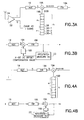
- Figs. 3A and 3B are more detailed block diagrams of the DC offset block 19B of Fig. 2B, and further illustrate a first embodiment of this invention wherein a negative feedback path exists around the FIR filter 18A.
- an integration block 23 has an input coupled to the output of the FIR filter 18A for integrating the filtered output signal over some period of time.
- the integration period may vary, and if a low frequency component is present the integration period is extended.
- a negative feedback loop is thus established such that as the DC offset value varies about zero, the value placed into the register 19B varies as well, always tending to drive the DC offset value back towards zero.
- the integration block 23 is capable of measuring the DC offset, which has a value less than one half of the ADC LSB, because the FIR filter 18A has gain in the pass band. Thus, by including DC integrator 23, which also has gain, better results are achieved.
- the invention does not require that a FIR be used, and other filter types could be used as well.
- a FIR Infinite Impulse Response
- IIR Infinite Impulse Response
- teachings of this invention find use in various types of signal paths, and are not limited for use with received signal paths of mobile stations, such as cellular telephones and personal communicators.
- mobile stations such as cellular telephones and personal communicators.
- the disclosed embodiments are particularly useful in CDMA mobile stations, including Wide Band CDMA mobile stations, wherein the ADCs may be specified to have a more limited range of bits than in some other types of mobile stations.
Landscapes
- Engineering & Computer Science (AREA)
- Theoretical Computer Science (AREA)
- Analogue/Digital Conversion (AREA)
- Digital Transmission Methods That Use Modulated Carrier Waves (AREA)
Abstract
Description
.., 001, 010, 011, 010, 000, 111, 111, 000, 010, 011, 010, 001, 000, 111, 111,.., etc.
.., 00001, 00101, 01001, 00101, 11101, 11001, 11001, 11101, 00101, 01001, 00001, 11101, 11001, 11001, 11101,.., (etc.)
..,1,5,9,5,-3,-7,-7,-3,5,9,5,1,-3,-7,-7,-3.., (etc.)
..,6,14,14,2,-10,-14,-10,2,14,14,6,-2,-10,-14,-10,-2,.., (etc.) which, when expressed in a 5-bit binary representation, is as follows (see also Fig. 2C):
.., 00110, 01110, 01110, 00010, 10110, 10010, 10110, 00001, 01110, 01110, 00110, 11110, 10110, 10010, 10110, 11110, ... (etc.)
Claims (20)
- A signal path, comprising:an analog to digital converter (ADC) for representing an input signal as n-bits, the n-bit representation comprising a DC offset component; anda summing node having a first input for inputting the n-bit output of the ADC and a second input for inputting a k-bit representation of a DC offset component compensation value, where k=n+m, where m is a number of bits that represent a value smaller than one least significant bit (LSB) of said n-bit representation, wherein said summing node operates to subtract the value appearing at said second input from the value appearing at said first input, and to output a k-bit DC offset compensated value.
- A signal path as in claim 1, and further comprising a filter coupled to the output of said summing node.
- A signal path as in claim 1, and further comprising a finite impulse response (FIR) filter coupled to the output of said summing node.
- A signal path as in claim 1, and further comprising an infinite impulse response (IIR) filter coupled to the output of said summing node.
- A signal path as in claim 2, and further comprising a negative feedback path from an output of said filter to said second input of said summing node for generating said k-bit representation of the DC offset component compensation value.
- A signal path as in claim 1, wherein said signal path comprises a signal path of a mobile station.
- A signal path as in claim 1, wherein said signal path comprises one of an Inphase (I) or a Quadrature (Q) signal path of a mobile station.
- A signal path, comprising:an analog to digital converter (ADC) for representing an input signal as n-bits, the n-bit representation comprising a DC offset component;a filter having an input coupled to an output of said ADC and an output for providing a filtered k-bit representation of said ADC output, where k=n+m, where m is a number of bits that represent a value smaller than one least significant bit (LSB) of said n-bit representation; anda summing node having a first input for inputting the k-bit output of said filter and a second input for inputting a k-bit representation of a DC offset component compensation value, wherein said summing node operates to subtract the value appearing at said second input from the value appearing at said first input, and to output a k-bit DC offset compensated value.
- A signal path as in claim 8, wherein said filter is comprised of a finite impulse response (FIR) filter.
- A signal path as in claim 8, wherein said filter is comprised of an infinite impulse response (IIR) filter.
- A signal path as in claim 8, and further comprising a negative feedback path from an output of said summing node to said second input of said summing node for generating said k-bit representation of the DC offset component compensation value.
- A signal path as in claim 8, wherein said signal path comprises a signal path of a mobile station.
- A signal path as in claim 8, wherein said signal path comprises one of an Inphase (I) or a Quadrature (Q) signal path of a mobile station.
- A method for removing a DC offset value in a signal path, comprising steps of:representing an input signal as n-bits, the n-bit representation comprising a DC offset component;subtracting from the n-bit representation a k-bit representation of a DC offset component compensation value, where k=n+m, where m is a number of bits that represent a value smaller than one least significant bit (LSB) of said n-bit representation;outputting a k-bit DC offset compensated value; andfiltering the k-bit DC offset compensated value.
- A method as in claim 14, where the step of filtering uses a finite impulse response (FIR) filter.
- A method as in claim 14, where the step of filtering uses an infinite impulse response (IIR) filter.
- A method for removing a DC offset value in a signal path, comprising steps of:representing an input signal as n-bits, the n-bit representation comprising a DC offset component;filtering said n-bit representation to provide a filtered k-bit representation of said n-bit representation, where k=n+m, where m is a number of bits that represent a value smaller than one least significant bit (LSB) of said n-bit representation; andsubtracting from the k-bit output of said filter a k-bit representation of a DC offset component compensation value for providing a k-bit DC offset compensated value.
- A method as in claim 17, where the step of filtering uses a finite impulse response (FIR) filter.
- A method as in claim 17, where the step of filtering uses an infinite impulse response (IIR) filter.
- Apparatus for removing a DC offset from a digital signal represented as n bits and including a DC offset component, comprising means (19A) for subtracting a digital compensation component corresponding to the DC offset from the digital signal, and means (18A) for filtering the digital signal characterised in that the offset compensation component comprises a k bit signal where K = m+n and m is a number of bits that represent a value smaller than one least significant bit of the n bit digital signal.
Priority Applications (2)
| Application Number | Priority Date | Filing Date | Title |
|---|---|---|---|
| EP07110473A EP1830469A1 (en) | 1999-12-07 | 2000-11-27 | Method and apparatus for digitally removing a DC-offset smaller than one LSB |
| EP07107155A EP1811672A1 (en) | 1999-12-07 | 2000-11-27 | Method and apparatus for digitally removing a DC-offset smaller than one LSB |
Applications Claiming Priority (2)
| Application Number | Priority Date | Filing Date | Title |
|---|---|---|---|
| US456758 | 1999-12-07 | ||
| US09/456,758 US6633618B1 (en) | 1999-12-07 | 1999-12-07 | Method and apparatus for digitally removing a DC-offset smaller than one LSB |
Related Child Applications (2)
| Application Number | Title | Priority Date | Filing Date |
|---|---|---|---|
| EP07110473A Division EP1830469A1 (en) | 1999-12-07 | 2000-11-27 | Method and apparatus for digitally removing a DC-offset smaller than one LSB |
| EP07107155A Division EP1811672A1 (en) | 1999-12-07 | 2000-11-27 | Method and apparatus for digitally removing a DC-offset smaller than one LSB |
Publications (3)
| Publication Number | Publication Date |
|---|---|
| EP1107459A2 true EP1107459A2 (en) | 2001-06-13 |
| EP1107459A3 EP1107459A3 (en) | 2003-09-10 |
| EP1107459B1 EP1107459B1 (en) | 2007-06-20 |
Family
ID=23814041
Family Applications (3)
| Application Number | Title | Priority Date | Filing Date |
|---|---|---|---|
| EP07107155A Withdrawn EP1811672A1 (en) | 1999-12-07 | 2000-11-27 | Method and apparatus for digitally removing a DC-offset smaller than one LSB |
| EP07110473A Withdrawn EP1830469A1 (en) | 1999-12-07 | 2000-11-27 | Method and apparatus for digitally removing a DC-offset smaller than one LSB |
| EP00310487A Expired - Lifetime EP1107459B1 (en) | 1999-12-07 | 2000-11-27 | Method and apparatus for digitally removing a DC-offset smaller than one LSB |
Family Applications Before (2)
| Application Number | Title | Priority Date | Filing Date |
|---|---|---|---|
| EP07107155A Withdrawn EP1811672A1 (en) | 1999-12-07 | 2000-11-27 | Method and apparatus for digitally removing a DC-offset smaller than one LSB |
| EP07110473A Withdrawn EP1830469A1 (en) | 1999-12-07 | 2000-11-27 | Method and apparatus for digitally removing a DC-offset smaller than one LSB |
Country Status (4)
| Country | Link |
|---|---|
| US (1) | US6633618B1 (en) |
| EP (3) | EP1811672A1 (en) |
| JP (1) | JP2001197137A (en) |
| DE (1) | DE60035249T2 (en) |
Cited By (1)
| Publication number | Priority date | Publication date | Assignee | Title |
|---|---|---|---|---|
| US6756924B2 (en) | 2002-05-16 | 2004-06-29 | Integrant Technologies Inc. | Circuit and method for DC offset calibration and signal processing apparatus using the same |
Families Citing this family (6)
| Publication number | Priority date | Publication date | Assignee | Title |
|---|---|---|---|---|
| GB2382331B (en) * | 1999-11-02 | 2003-10-01 | Allan William Stobart | Improvements in and relating to road and rail tankers |
| US7295634B2 (en) * | 2000-12-27 | 2007-11-13 | Intel Corporation | Portable communication device and method therefor |
| KR20030015933A (en) * | 2001-08-18 | 2003-02-26 | 엘지전자 주식회사 | Digital dc offset compensator |
| US7336937B2 (en) | 2004-05-05 | 2008-02-26 | Nokia Corporation | Compensation of a DC offset in a receiver |
| GB0803710D0 (en) | 2008-02-28 | 2008-04-09 | Nokia Corp | DC compensation |
| CN111061422B (en) * | 2019-12-13 | 2022-09-02 | 明见(厦门)技术有限公司 | Approximation type direct current component extraction method, terminal equipment and storage medium |
Family Cites Families (7)
| Publication number | Priority date | Publication date | Assignee | Title |
|---|---|---|---|---|
| US5153593A (en) * | 1990-04-26 | 1992-10-06 | Hughes Aircraft Company | Multi-stage sigma-delta analog-to-digital converter |
| US5281968A (en) * | 1991-09-06 | 1994-01-25 | Nec Corporation | DC offset correction circuit for A/D converter |
| US5465092A (en) * | 1994-01-19 | 1995-11-07 | National Semiconductor Corporation | Pipelined analog-to-digital converter with curvefit digital correction |
| US6100827A (en) * | 1998-09-11 | 2000-08-08 | Ericsson Inc. | Modulation systems and methods that compensate for DC offset introduced by the digital-to-analog converter and/or the low pass filter thereof |
| JPH11341447A (en) * | 1998-05-27 | 1999-12-10 | Mitsubishi Electric Corp | Data slice apparatus and data slice method |
| SE514770C2 (en) * | 1999-05-25 | 2001-04-23 | Ericsson Telefon Ab L M | Procedure and arrangement for correcting offset errors in A / D conversion |
| US6166668A (en) * | 1999-06-01 | 2000-12-26 | Motorola, Inc. | Method and apparatus for providing DC offset correction and hold capability |
-
1999
- 1999-12-07 US US09/456,758 patent/US6633618B1/en not_active Expired - Lifetime
-
2000
- 2000-11-27 EP EP07107155A patent/EP1811672A1/en not_active Withdrawn
- 2000-11-27 DE DE60035249T patent/DE60035249T2/en not_active Expired - Lifetime
- 2000-11-27 EP EP07110473A patent/EP1830469A1/en not_active Withdrawn
- 2000-11-27 EP EP00310487A patent/EP1107459B1/en not_active Expired - Lifetime
- 2000-12-01 JP JP2000366721A patent/JP2001197137A/en active Pending
Cited By (1)
| Publication number | Priority date | Publication date | Assignee | Title |
|---|---|---|---|---|
| US6756924B2 (en) | 2002-05-16 | 2004-06-29 | Integrant Technologies Inc. | Circuit and method for DC offset calibration and signal processing apparatus using the same |
Also Published As
| Publication number | Publication date |
|---|---|
| DE60035249T2 (en) | 2008-02-21 |
| JP2001197137A (en) | 2001-07-19 |
| DE60035249D1 (en) | 2007-08-02 |
| EP1811672A1 (en) | 2007-07-25 |
| EP1830469A1 (en) | 2007-09-05 |
| EP1107459A3 (en) | 2003-09-10 |
| US6633618B1 (en) | 2003-10-14 |
| EP1107459B1 (en) | 2007-06-20 |
Similar Documents
| Publication | Publication Date | Title |
|---|---|---|
| AU689500B2 (en) | Apparatus for and method of speech digitizing | |
| KR100562730B1 (en) | D.C. of digital-to-analog converter comparing input signal and output signal of converter. Offset correction | |
| US6606359B1 (en) | Area-optimum rapid acquisition cellular multi-protocol digital DC offset correction scheme | |
| US6894627B2 (en) | Increasing the SNR of successive approximation type ADCs without compromising throughput performance substantially | |
| US5880973A (en) | Signal processing system and method for enhanced cascaded integrator-comb interpolation filter stabilization | |
| WO1989007862A1 (en) | Digital to analogue converter | |
| JP2001518734A (en) | Method and apparatus for determining received signal strength | |
| US6633618B1 (en) | Method and apparatus for digitally removing a DC-offset smaller than one LSB | |
| US10630309B1 (en) | Signal receiver for radio signal strength indication estimation with sub-sampling analog-to-digital converter for radio frequency signal with constant envelope modulation | |
| US7317904B2 (en) | DC offset cancel circuit | |
| JP3956582B2 (en) | A / D conversion circuit | |
| KR100227173B1 (en) | Bit series digital compressor | |
| HK1039410A (en) | Method and apparatus for digitally removing a dc-offset smaller than one lsb | |
| US6933874B2 (en) | Applying desired voltage at a node | |
| US7425911B2 (en) | Signal-to-noise ratio when using fewer bits than the number of output bits of an analog to digital converter | |
| US6847321B1 (en) | Closed loop amplification with high throughput performance | |
| US20020003485A1 (en) | Method of performing A/D conversion, and an A/D converter | |
| JPH01117527A (en) | Code converter | |
| US6741200B2 (en) | Method and apparatus of stage amplifier of analog to digital converter | |
| US7330520B2 (en) | Reduced size and power demapper for viterbi decoding | |
| JPH09512413A (en) | Method and apparatus for reducing quantization noise | |
| WO2006124168A1 (en) | Digital automatic gain control method and device | |
| US20090091487A1 (en) | Spurious Free Dynamic Range Of An Analog To Digital Converter | |
| JP3123941B2 (en) | Baseband signal processing circuit for quadrature signal demodulation | |
| JP2000224047A (en) | Digital signal processing circuit |
Legal Events
| Date | Code | Title | Description |
|---|---|---|---|
| PUAI | Public reference made under article 153(3) epc to a published international application that has entered the european phase |
Free format text: ORIGINAL CODE: 0009012 |
|
| AK | Designated contracting states |
Kind code of ref document: A2 Designated state(s): AT BE CH CY DE DK ES FI FR GB GR IE IT LI LU MC NL PT SE TR |
|
| AX | Request for extension of the european patent |
Free format text: AL;LT;LV;MK;RO;SI |
|
| RAP1 | Party data changed (applicant data changed or rights of an application transferred) |
Owner name: NOKIA CORPORATION |
|
| PUAL | Search report despatched |
Free format text: ORIGINAL CODE: 0009013 |
|
| AK | Designated contracting states |
Kind code of ref document: A3 Designated state(s): AT BE CH CY DE DK ES FI FR GB GR IE IT LI LU MC NL PT SE TR |
|
| AX | Request for extension of the european patent |
Extension state: AL LT LV MK RO SI |
|
| 17P | Request for examination filed |
Effective date: 20040205 |
|
| AKX | Designation fees paid |
Designated state(s): DE FI FR GB NL |
|
| 17Q | First examination report despatched |
Effective date: 20040706 |
|
| GRAP | Despatch of communication of intention to grant a patent |
Free format text: ORIGINAL CODE: EPIDOSNIGR1 |
|
| GRAS | Grant fee paid |
Free format text: ORIGINAL CODE: EPIDOSNIGR3 |
|
| GRAA | (expected) grant |
Free format text: ORIGINAL CODE: 0009210 |
|
| AK | Designated contracting states |
Kind code of ref document: B1 Designated state(s): DE FI FR GB NL |
|
| REG | Reference to a national code |
Ref country code: GB Ref legal event code: FG4D |
|
| REF | Corresponds to: |
Ref document number: 60035249 Country of ref document: DE Date of ref document: 20070802 Kind code of ref document: P |
|
| EN | Fr: translation not filed | ||
| PLBE | No opposition filed within time limit |
Free format text: ORIGINAL CODE: 0009261 |
|
| STAA | Information on the status of an ep patent application or granted ep patent |
Free format text: STATUS: NO OPPOSITION FILED WITHIN TIME LIMIT |
|
| PGFP | Annual fee paid to national office [announced via postgrant information from national office to epo] |
Ref country code: FR Payment date: 20071108 Year of fee payment: 8 Ref country code: GB Payment date: 20071121 Year of fee payment: 8 |
|
| 26N | No opposition filed |
Effective date: 20080325 |
|
| REG | Reference to a national code |
Ref country code: HK Ref legal event code: WD Ref document number: 1039410 Country of ref document: HK |
|
| PG25 | Lapsed in a contracting state [announced via postgrant information from national office to epo] |
Ref country code: FR Free format text: LAPSE BECAUSE OF FAILURE TO SUBMIT A TRANSLATION OF THE DESCRIPTION OR TO PAY THE FEE WITHIN THE PRESCRIBED TIME-LIMIT Effective date: 20080222 |
|
| PG25 | Lapsed in a contracting state [announced via postgrant information from national office to epo] |
Ref country code: FI Free format text: LAPSE BECAUSE OF FAILURE TO SUBMIT A TRANSLATION OF THE DESCRIPTION OR TO PAY THE FEE WITHIN THE PRESCRIBED TIME-LIMIT Effective date: 20070620 |
|
| GBPC | Gb: european patent ceased through non-payment of renewal fee |
Effective date: 20081127 |
|
| PG25 | Lapsed in a contracting state [announced via postgrant information from national office to epo] |
Ref country code: GB Free format text: LAPSE BECAUSE OF NON-PAYMENT OF DUE FEES Effective date: 20081127 |
|
| REG | Reference to a national code |
Ref country code: DE Ref legal event code: R082 Ref document number: 60035249 Country of ref document: DE Representative=s name: EISENFUEHR SPEISER PATENTANWAELTE RECHTSANWAEL, DE Ref country code: DE Ref legal event code: R081 Ref document number: 60035249 Country of ref document: DE Owner name: NOKIA TECHNOLOGIES OY, FI Free format text: FORMER OWNER: NOKIA CORP., 02610 ESPOO, FI |
|
| REG | Reference to a national code |
Ref country code: NL Ref legal event code: PD Owner name: NOKIA TECHNOLOGIES OY; FI Free format text: DETAILS ASSIGNMENT: VERANDERING VAN EIGENAAR(S), OVERDRACHT; FORMER OWNER NAME: NOKIA CORPORATION Effective date: 20151111 |
|
| PGFP | Annual fee paid to national office [announced via postgrant information from national office to epo] |
Ref country code: NL Payment date: 20181114 Year of fee payment: 19 |
|
| PGFP | Annual fee paid to national office [announced via postgrant information from national office to epo] |
Ref country code: DE Payment date: 20181113 Year of fee payment: 19 |
|
| REG | Reference to a national code |
Ref country code: DE Ref legal event code: R119 Ref document number: 60035249 Country of ref document: DE |
|
| REG | Reference to a national code |
Ref country code: NL Ref legal event code: MM Effective date: 20191201 |
|
| PG25 | Lapsed in a contracting state [announced via postgrant information from national office to epo] |
Ref country code: NL Free format text: LAPSE BECAUSE OF NON-PAYMENT OF DUE FEES Effective date: 20191201 |
|
| PG25 | Lapsed in a contracting state [announced via postgrant information from national office to epo] |
Ref country code: DE Free format text: LAPSE BECAUSE OF NON-PAYMENT OF DUE FEES Effective date: 20200603 |