EP1107326A1 - Laminated piezoelectric transducer - Google Patents
Laminated piezoelectric transducer Download PDFInfo
- Publication number
- EP1107326A1 EP1107326A1 EP00925605A EP00925605A EP1107326A1 EP 1107326 A1 EP1107326 A1 EP 1107326A1 EP 00925605 A EP00925605 A EP 00925605A EP 00925605 A EP00925605 A EP 00925605A EP 1107326 A1 EP1107326 A1 EP 1107326A1
- Authority
- EP
- European Patent Office
- Prior art keywords
- piezoelectric transformer
- internal electrodes
- laminated body
- transformer according
- thickness
- Prior art date
- Legal status (The legal status is an assumption and is not a legal conclusion. Google has not performed a legal analysis and makes no representation as to the accuracy of the status listed.)
- Withdrawn
Links
Images




Classifications
-
- H—ELECTRICITY
- H10—SEMICONDUCTOR DEVICES; ELECTRIC SOLID-STATE DEVICES NOT OTHERWISE PROVIDED FOR
- H10N—ELECTRIC SOLID-STATE DEVICES NOT OTHERWISE PROVIDED FOR
- H10N30/00—Piezoelectric or electrostrictive devices
- H10N30/40—Piezoelectric or electrostrictive devices with electrical input and electrical output, e.g. functioning as transformers
-
- H—ELECTRICITY
- H10—SEMICONDUCTOR DEVICES; ELECTRIC SOLID-STATE DEVICES NOT OTHERWISE PROVIDED FOR
- H10N—ELECTRIC SOLID-STATE DEVICES NOT OTHERWISE PROVIDED FOR
- H10N30/00—Piezoelectric or electrostrictive devices
- H10N30/50—Piezoelectric or electrostrictive devices having a stacked or multilayer structure
-
- H—ELECTRICITY
- H10—SEMICONDUCTOR DEVICES; ELECTRIC SOLID-STATE DEVICES NOT OTHERWISE PROVIDED FOR
- H10N—ELECTRIC SOLID-STATE DEVICES NOT OTHERWISE PROVIDED FOR
- H10N30/00—Piezoelectric or electrostrictive devices
- H10N30/50—Piezoelectric or electrostrictive devices having a stacked or multilayer structure
- H10N30/501—Piezoelectric or electrostrictive devices having a stacked or multilayer structure having a non-rectangular cross-section in a plane parallel to the stacking direction, e.g. polygonal or trapezoidal in side view
-
- H—ELECTRICITY
- H10—SEMICONDUCTOR DEVICES; ELECTRIC SOLID-STATE DEVICES NOT OTHERWISE PROVIDED FOR
- H10N—ELECTRIC SOLID-STATE DEVICES NOT OTHERWISE PROVIDED FOR
- H10N30/00—Piezoelectric or electrostrictive devices
- H10N30/80—Constructional details
- H10N30/85—Piezoelectric or electrostrictive active materials
- H10N30/853—Ceramic compositions
-
- H—ELECTRICITY
- H10—SEMICONDUCTOR DEVICES; ELECTRIC SOLID-STATE DEVICES NOT OTHERWISE PROVIDED FOR
- H10N—ELECTRIC SOLID-STATE DEVICES NOT OTHERWISE PROVIDED FOR
- H10N30/00—Piezoelectric or electrostrictive devices
- H10N30/80—Constructional details
- H10N30/87—Electrodes or interconnections, e.g. leads or terminals
- H10N30/871—Single-layered electrodes of multilayer piezoelectric or electrostrictive devices, e.g. internal electrodes
-
- H—ELECTRICITY
- H10—SEMICONDUCTOR DEVICES; ELECTRIC SOLID-STATE DEVICES NOT OTHERWISE PROVIDED FOR
- H10N—ELECTRIC SOLID-STATE DEVICES NOT OTHERWISE PROVIDED FOR
- H10N30/00—Piezoelectric or electrostrictive devices
- H10N30/80—Constructional details
- H10N30/87—Electrodes or interconnections, e.g. leads or terminals
- H10N30/877—Conductive materials
Definitions
- the present invention relates to a laminated piezoelectric transformers for use in cold-cathode-tube inverter circuits, which are used in electronic apparatuses having a liquid crystal screen such as personal computers , portable information terminals and video movies, for stepping up voltages and lighting/dimming the cold cathode tube or for use in other voltage stepping up circuits.
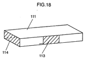
- FIG. 18 is a perspective view of a conventional laminated piezoelectric transformer.
- ceramic layers 111 and input side internal electrodes are alternately laminated to form a laminated body in a rectangular parallelepiped shape.
- the internal electrodes on the input side are arranged to be alternately exposed on the opposite side faces of the laminated body at the middle portion along the longitudinal direction of the laminated body.
- a laminated piezoelectric transformer according to the present invention comprises:
- the internal electrodes of the laminated piezoelectric transformer of the invention are characterized by having a plurality of primary internal electrodes disposed at the middle portion along the longitudinal direction of the laminated body and a plurality of secondary internal electrodes disposed at opposite end portions of the laminated body with respect to the longitudinal direction.
- the laminated piezoelectric transformer of the present invention comprises:
- Another laminated piezoelectric transformer of the present invention is characterized by having a plurality of primary internal electrodes extending from the middle portion along the longitudinal direction of the laminated body to the vicinity of one end portion in the longitudinal direction of the same and a plurality of secondary internal electrodes disposed at another end portion of the laminated body.
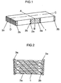
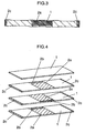
- the laminated piezoelectric transformer according to the first exemplary embodiment of the invention comprises ceramic layer 1, primary internal electrodes 2a, 2b, secondary internal electrode 2c, primary external electrode 3a, and secondary external electrode 3b. Processes for fabricating the same will be described in accordance with a fabrication flowchart shown in FIG. 5.
- PbO, ZrO2, TiO2 were used as the main raw materials and a predetermined proportion of sub raw materials were added thereto (100). The materials were then mixed in a ball mill for a predetermined period of time (101).
- the mixed material powder were calcined (102), mixed with predetermined amounts of organic binder, plasticizer, and organic solvent, and were subjected to slurry mixing (103) to obtain slurry for forming sheets.
- sheet formation was carried out by coating the slurry with a doctor blade method (104) to obtain ceramic sheet 1 of a predetermined thickness.
- the internal-electrode paste was printed on ceramic sheet 1 to form primary internal electrode 2a, 2b and secondary internal electrode 2c of the shapes shown in FIG. 4 (105).
- the internal-electrode paste contains Ag-Pd as the main components and contains the raw material powders of the ceramic sheet, at least, as the sub components.
- primary internal electrodes 2a and 2b are placed such that they are opposite to each other at the middle portion along the longitudinal direction of one layer of ceramic layer 1 and their edge portions are exposed on both side faces with respect to the transverse direction of the laminated body.
- secondary internal electrodes 2c were formed at both end portions in the longitudinal direction of one layer of ceramic layer 1 such that they are exposed on both side faces in the transverse direction of the laminated body to be formed later.
- the organic binder within the laminated body was burned out to be removed and, thereafter, the laminated body was sintered one hour at the temperatures of 1000 - 1200 °C (107).
- the overall outer surface of the laminated body was polished such that end portions are given a curved shape and primary and secondary internal electrodes 2a, 2b, 2c are completely exposed on the outer surface of the laminated body.
- primary external electrodes 3a were formed on both side faces of the laminated body where internal electrodes 2a, 2b are exposed; and secondary external electrodes 3b were formed on the end faces of the laminated body where internal electrodes 2c are exposed (109).
- FIG. 6 is a perspective view of a laminated piezoelectric transformer according to the second exemplary embodiment.
- external electrode 3a and external electrode 3b were only formed on the side faces in the transverse direction of the laminated body.
- external electrode 3a and external electrode 3b are formed not only on the side face but also on the top and bottom faces of the laminated body.
- outermost ceramic layers 1 constituting the top and bottom surfaces of the laminated body are also polarized by external electrodes 3a, 3b, the voltage step-up ratio is improved.
- external electrodes 3a, 3b formed on the surface of the laminated body be as large as possible.
- the steps down to the ceramic sheet formation are the same as in the first exemplary embodiment.
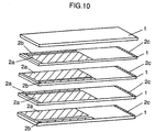
- the internal-electrode paste was printed on the ceramic sheet to obtain primary and secondary internal electrodes 2a, 2b, 2c (205) of the shapes as shown in FIG. 10.
- the internal-electrode paste contains Ag-Pd as the major components and the raw material powder of the ceramic sheet, at least, as the sub components.
- primary internal electrodes 2a, 2b were disposed to extend from the middle portion along the longitudinal direction of one layer of ceramic layer 1 to its one end portion as shown in FIG. 10.
- Internal electrodes 2a and 2b were arranged to be opposite to each other with respect to the transverse direction and to have their end portions exposed on both side faces of the laminated body in the transverse direction.
- internal electrodes 2a and 2b were arranged not to expose on the end faces in the longitudinal direction.
- the laminated body was sintered (207) and overall external surface was subjected to polishing (208).
- primary external electrodes 3a were formed on both side faces of the laminated body in the transverse direction where internal electrodes 2a, 2b are exposed. Further, secondary external electrode 3b was formed on the side faces of the laminated body in the transverse direction where internal electrode 2c is exposed (209).
- ceramic layer 1 between internal electrodes 3a was polarized and the overall ceramic layer 1 was polarized (210) to obtain a laminated piezoelectric transformer.
- FIG. 12 is a perspective view of a laminated piezoelectric transformer according to the fourth exemplary embodiment.
- external electrode 3a and external electrode 3b in the third exemplary embodiment, were formed only on the side face of the laminated body in the transverse direction, primary and secondary external electrodes 3a, 3b in the present exemplary embodiment are formed not only on the side faces of the laminated body but also on both top and bottom surfaces of the laminated body.
- the adhesive strength between the laminated body and external electrodes 3a, 3b are increased and, also, the strength of the laminated body is increased.
- the voltage step-up ratio is improved.
- external electrodes 3a, 3b on the input side and output side formed on the surface of the laminated body be as large as possible.
- a laminated piezoelectric transformer capable of stepping up voltage at high energy conversion efficiency can be provided. Accordingly, by the use of the laminated piezoelectric transformer of the invention, power consumption in electronic devices can be decreased.
Landscapes
- Engineering & Computer Science (AREA)
- Power Engineering (AREA)
- Chemical & Material Sciences (AREA)
- Ceramic Engineering (AREA)
- Dc-Dc Converters (AREA)
- Piezo-Electric Transducers For Audible Bands (AREA)
Abstract
Description
- 1
- ceramic layer
- 2a
- primary internal electrode
- 2b
- primary internal electrode
- 2c
- primary internal electrode
- 3a
- primary external electrode
- 3a
- secondary external electrode
- 200
- case
- 201
- conductive rubber
Claims (34)
- A laminated piezoelectric transformer comprising:a laminated body formed by laminating a plurality of ceramic layers and a plurality of internal electrodes; anda plurality of external electrodes electrically connected with said internal electrodes; whereinsaid internal electrodes havea plurality of primary internal electrodes disposed at a middle portion along a longitudinal direction of said laminated body anda plurality of secondary internal electrodes disposed at both end portions in the longitudinal direction of said laminated body.
- The piezoelectric transformer according to claim 1, wherein a length of a portion where said internal electrodes are not formed in a transverse direction of said laminated body is smaller than a length of the portion where said internal electrodes are formed in the transverse direction of said laminated body.
- The piezoelectric transformer according to claim 1, wherein a thickness of the laminated body at a portion where said internal electrodes are not formed is smaller than a thickness of the laminated body at a portion where said internal electrodes are formed.
- The piezoelectric transformer according to claim 1, wherein said primary internal electrodes are made up of at least two internal electrodes formed on the same plane.
- The piezoelectric transformer according to claim 4, wherein a relationship between a thickness of a ceramic layer at a portion between said primary internal electrodes and a distance between said primary internal electrodes formed on a same plane is given by t/4 < x,
where, t is the thickness of the ceramic layer, and x is the distance between said primary internal electrodes - The piezoelectric transformer according to claim 1, wherein two or more edge portions of said plurality of primary internal electrodes do not exist on the same plane taken in a direction of a thickness of said laminated body .
- The piezoelectric transformer according to claim 1, wherein said plurality of external electrodes are formed on a same side face of said laminated body.
- The piezoelectric transformer according to claim 1, wherein said plurality of external electrodes are formed on a same side face of said laminated body and at least on a part of top and bottom faces of said laminated body.
- The piezoelectric transformer according to claim 1, wherein a surface of said internal electrode is a rough surface.
- The piezoelectric transformer according to claim 1, wherein said internal electrode includes components of said ceramic layer.
- The piezoelectric transformer according to claim 1, wherein a average grain size of components constituting said ceramic layer is larger than a average grain size of metallic components of said internal electrode.
- The piezoelectric transformer according to claim 1, wherein a surface of a end portion of said laminated body is a curved surface.
- The piezoelectric transformer according to claim 1, wherein the internal electrode has a curved portion at a circumferential portion thereof.
- The piezoelectric transformer according to claim 1, wherein an average grain size of components constituting said ceramic layer at a portion where said internal electrodes are not formed is larger than a average grain size of the component constituting said ceramic layer at a portion between said primary internal electrodes.
- The piezoelectric transformer according to claim 1, wherein a thickness of a ceramic layer from a surface of said laminated body to said primary internal electrode or said secondary internal electrode in a shortest distance therefrom is arranged to be equal to or smaller than a thickness of a ceramic layer at a portion between said internal electrodes.
- The piezoelectric transformer according to claim 1, wherein angles between each of adjoining sides of the cross-section of said laminated body are non-rectangular.
- The piezoelectric transformer according to claim 1, wherein a thickness of said internal electrode at a circumferential portion is smaller than a thickness of the same at the middle portion.
- A laminated piezoelectric transformer comprising:a laminated body formed by laminating a plurality of ceramic layers and a plurality of internal electrodes; anda plurality of external electrodes electrically connected with said internal electrodes and disposed on the surface of said laminated body, whereinsaid internal electrodes are made up ofa plurality of primary internal electrodes arranged to extend from a middle portion along a longitudinal direction of said laminated body to a vicinity of one end portion in the longitudinal direction of the same, anda plurality of secondary internal electrodes disposed at another end portion in the longitudinal direction of said laminated body.
- The piezoelectric transformer according to claim 18, wherein a length of a portion where said internal electrodes are not formed in a transverse direction of said laminated body is smaller than a length of the portion where said internal electrodes are formed in the transverse direction of said laminated body.
- The piezoelectric transformer according to claim 18, wherein a thickness of the laminated body at the portion where said internal electrodes are not formed is smaller than a thickness of the laminated body at the portion where said internal electrodes are formed.
- The piezoelectric transformer according to claim 18, wherein said primary internal electrodes are made up of at least two internal electrodes formed on a same plane.
- The piezoelectric transformer according to claim 21, wherein a relationship between a thickness of the ceramic layer at the portion between said primary internal electrodes, and a distance between said primary internal electrodes formed on a same plane, is given by t/4 < x, where t is the thickness of the ceramic layer and x is the distance between said primary internal electrodes.
- The piezoelectric transformer according to claim 18, wherein two or more edge portions of said plurality of primary internal electrodes do not exist on a same plane taken in a direction of the thickness of said laminated body.
- The piezoelectric transformer according to claim 18, wherein said plurality of external electrodes are formed on a same side face of said laminated body.
- The piezoelectric transformer according to claim 18, wherein said plurality of external electrodes are formed on a same side face of said laminated body and at least at part of top and bottom faces of said laminated body.
- The piezoelectric transformer according to claim 18, wherein a surface of said internal electrode is a rough surface.
- The piezoelectric transformer according to claim 18, wherein said internal electrode contains components of said ceramic layer.
- The piezoelectric transformer according to claim 18, wherein the average grain side of the components constituting said ceramic layer is larger than the average grain side of metallic components of said internal electrode.
- The piezoelectric transformer according to claim 18, wherein a surface of end portion of said laminated body is a curved surface.
- The piezoelectric transformer according to claim 18, wherein the internal electrode has a curved portion at a circumferential portion thereof.
- The piezoelectric transformer according to claim 18, wherein an average grain size of components constituting said ceramic layer at a portion where said internal electrodes are not formed is larger than a average grain size of the component constituting said ceramic layer at a portion between said primary internal electrodes.
- The piezoelectric transformer according to claim 18, wherein a thickness of a ceramic layer from the surface of said laminated body to said primary internal electrode or said secondary internal electrode in the shortest distance therefrom is arranged to be equal to or smaller than a thickness of the ceramic layer at a portion between said internal electrodes.
- The piezoelectric transformer according to claim 18, wherein angles between each of adjoining sides of the cross-section of said laminated body are non-rectangular.
- The piezoelectric transformer according to claim 18, wherein a thickness of said internal electrode at the circumferential portion is smaller than a thickness of the same at the middle portion.
Applications Claiming Priority (3)
| Application Number | Priority Date | Filing Date | Title |
|---|---|---|---|
| JP13091699A JP3551078B2 (en) | 1999-05-12 | 1999-05-12 | Multilayer piezoelectric transformer and electronic equipment using it |
| JP13091699 | 1999-05-12 | ||
| PCT/JP2000/003001 WO2000070688A1 (en) | 1999-05-12 | 2000-05-11 | Laminated piezoelectric transducer |
Publications (2)
| Publication Number | Publication Date |
|---|---|
| EP1107326A1 true EP1107326A1 (en) | 2001-06-13 |
| EP1107326A4 EP1107326A4 (en) | 2007-04-11 |
Family
ID=15045745
Family Applications (1)
| Application Number | Title | Priority Date | Filing Date |
|---|---|---|---|
| EP00925605A Withdrawn EP1107326A4 (en) | 1999-05-12 | 2000-05-11 | PIEZOELECTRIC TRANSDUCER LAMINATE |
Country Status (6)
| Country | Link |
|---|---|
| US (1) | US6448698B1 (en) |
| EP (1) | EP1107326A4 (en) |
| JP (1) | JP3551078B2 (en) |
| CN (1) | CN1172381C (en) |
| TW (1) | TW463397B (en) |
| WO (1) | WO2000070688A1 (en) |
Cited By (1)
| Publication number | Priority date | Publication date | Assignee | Title |
|---|---|---|---|---|
| EP1672710A4 (en) * | 2003-09-30 | 2008-03-19 | Taiheiyo Cement Corp | Piezoelectric transformer |
Families Citing this family (5)
| Publication number | Priority date | Publication date | Assignee | Title |
|---|---|---|---|---|
| EP1533896B1 (en) * | 2003-11-20 | 2011-11-02 | Panasonic Corporation | Piezoelectric element, composite piezoelectric element, and filter, duplexer and communication equipment using the same |
| CN103155191B (en) * | 2010-11-01 | 2016-01-20 | 株式会社村田制作所 | Multilayer piezoelectric actuator and piezoelectric vibrating device |
| US9579691B2 (en) | 2013-05-21 | 2017-02-28 | Mplus Co., Ltd. | Piezoelectric element and electronic component including the same |
| KR101662126B1 (en) * | 2014-05-02 | 2016-10-05 | 주식회사 엠플러스 | Vibrator |
| DE102014110405A1 (en) * | 2014-07-23 | 2016-01-28 | Epcos Ag | Piezoelectric transformer |
Family Cites Families (11)
| Publication number | Priority date | Publication date | Assignee | Title |
|---|---|---|---|---|
| EP0605901B1 (en) * | 1992-12-31 | 1996-10-09 | Nec Corporation | A piezoelectric transformer having improved electrode arrangement |
| JP2606667B2 (en) * | 1994-07-22 | 1997-05-07 | 日本電気株式会社 | Piezoelectric transformer and driving method thereof |
| JP3119154B2 (en) * | 1995-07-06 | 2000-12-18 | 日立金属株式会社 | Piezoelectric transformer and power conversion device using the same |
| JP3090023B2 (en) * | 1996-02-14 | 2000-09-18 | 株式会社村田製作所 | Multilayer piezoelectric transformer |
| JP2842382B2 (en) * | 1996-06-11 | 1999-01-06 | 日本電気株式会社 | Laminated piezoelectric transformer and method of manufacturing the same |
| TW432730B (en) * | 1996-07-12 | 2001-05-01 | Taiheiyo Cement Corp | Piezoelectric transformer device |
| JP3849190B2 (en) | 1996-12-11 | 2006-11-22 | 株式会社村田製作所 | Piezoelectric transformer |
| JPH114026A (en) | 1997-04-18 | 1999-01-06 | Nec Corp | Multilayer piezoelectric transformer |
| JP3468043B2 (en) | 1997-08-15 | 2003-11-17 | 日立金属株式会社 | Multilayer piezoelectric transformer |
| JP4030190B2 (en) * | 1998-06-18 | 2008-01-09 | 株式会社日本自動車部品総合研究所 | Piezoelectric ceramic composition and piezoelectric transformer |
| JP3457899B2 (en) * | 1998-11-18 | 2003-10-20 | 太陽誘電株式会社 | Piezoelectric transformer |
-
1999
- 1999-05-12 JP JP13091699A patent/JP3551078B2/en not_active Expired - Fee Related
-
2000
- 2000-05-11 CN CNB008008388A patent/CN1172381C/en not_active Expired - Fee Related
- 2000-05-11 TW TW089109016A patent/TW463397B/en not_active IP Right Cessation
- 2000-05-11 US US09/743,421 patent/US6448698B1/en not_active Expired - Fee Related
- 2000-05-11 WO PCT/JP2000/003001 patent/WO2000070688A1/en not_active Ceased
- 2000-05-11 EP EP00925605A patent/EP1107326A4/en not_active Withdrawn
Cited By (1)
| Publication number | Priority date | Publication date | Assignee | Title |
|---|---|---|---|---|
| EP1672710A4 (en) * | 2003-09-30 | 2008-03-19 | Taiheiyo Cement Corp | Piezoelectric transformer |
Also Published As
| Publication number | Publication date |
|---|---|
| WO2000070688A1 (en) | 2000-11-23 |
| US6448698B1 (en) | 2002-09-10 |
| CN1304555A (en) | 2001-07-18 |
| JP3551078B2 (en) | 2004-08-04 |
| EP1107326A4 (en) | 2007-04-11 |
| CN1172381C (en) | 2004-10-20 |
| JP2000323765A (en) | 2000-11-24 |
| TW463397B (en) | 2001-11-11 |
Similar Documents
| Publication | Publication Date | Title |
|---|---|---|
| EP0914681B1 (en) | Piezoelectric transformer device | |
| US5892318A (en) | Piezoelectric transformer with multiple output | |
| US7075217B2 (en) | Laminated piezoelectric transformer | |
| KR100317892B1 (en) | Piezoelectric transformer element and method of manufacturing the same | |
| US6448698B1 (en) | Laminated piezoelectric transformer | |
| KR100298281B1 (en) | Laminated piezoelectric transformer | |
| US7651655B2 (en) | Production methods of dielectric layer and dielectric element, dielectric element, and piezoelectric transformer | |
| EP1025597B1 (en) | Piezoelectric transformer element | |
| JP3334651B2 (en) | Piezoelectric transformer and method of manufacturing the same | |
| JP2907153B2 (en) | Piezoelectric transformer and method of manufacturing the same | |
| JP2000244033A (en) | Multilayer piezoelectric transformer | |
| JP3709114B2 (en) | Piezoelectric transformer | |
| JP3085595B2 (en) | Piezoelectric actuator and method of manufacturing the same | |
| JP2003008098A (en) | Multilayer piezoelectric transformer | |
| JP2001024247A (en) | Multilayer piezoelectric transformer and electronic equipment using the same | |
| JP3080033B2 (en) | Multilayer piezoelectric transformer | |
| JP2000294851A (en) | Multilayer piezoelectric electronic device | |
| HK1038097A (en) | Laminated piezoelectric transducer | |
| JP2003142747A (en) | Multilayer piezoelectric transformer | |
| JP2004335939A (en) | Rosen type piezoelectric transformer | |
| JPH1051044A (en) | Lamination type piezoelectric transformer element | |
| JP2001024246A (en) | Piezoelectric transformer element | |
| JP2002305332A (en) | Piezoelectric transformer | |
| JPH11298057A (en) | Piezoelectric transformer | |
| HK1031272B (en) | Piezoelectric transformer device |
Legal Events
| Date | Code | Title | Description |
|---|---|---|---|
| PUAI | Public reference made under article 153(3) epc to a published international application that has entered the european phase |
Free format text: ORIGINAL CODE: 0009012 |
|
| 17P | Request for examination filed |
Effective date: 20010131 |
|
| AK | Designated contracting states |
Kind code of ref document: A1 Designated state(s): AT BE CH CY DE DK ES FI FR GB GR IE IT LI LU MC NL PT SE |
|
| RBV | Designated contracting states (corrected) |
Designated state(s): DE FR GB |
|
| RIN1 | Information on inventor provided before grant (corrected) |
Inventor name: FUKUSHIMA, HIROSHI Inventor name: GOTO, YASUSHI Inventor name: OKUDA, KAZUHIRO Inventor name: KAWANO, KUNITOSHI Inventor name: YAMAGUCHI, TOMOKAZU Inventor name: KAWAMURA, SATOSHI Inventor name: MINAMI, SEIICHI |
|
| RIN1 | Information on inventor provided before grant (corrected) |
Inventor name: FUKUSHIMA, HIROSHI Inventor name: MINAMI, SEIICHI Inventor name: YAMAGUCHI, TOMOKAZU Inventor name: KAWANO, KUNITOSHI Inventor name: GOTO, YASUSHI Inventor name: OKUDA, KAZUHIRO Inventor name: KAWAMURA, SATOSHI |
|
| A4 | Supplementary search report drawn up and despatched |
Effective date: 20070314 |
|
| STAA | Information on the status of an ep patent application or granted ep patent |
Free format text: STATUS: THE APPLICATION HAS BEEN WITHDRAWN |
|
| 18W | Application withdrawn |
Effective date: 20070420 |