EP1107301B1 - Methods for cleaning substrate surfaces after etch operations - Google Patents
Methods for cleaning substrate surfaces after etch operations Download PDFInfo
- Publication number
- EP1107301B1 EP1107301B1 EP00310491A EP00310491A EP1107301B1 EP 1107301 B1 EP1107301 B1 EP 1107301B1 EP 00310491 A EP00310491 A EP 00310491A EP 00310491 A EP00310491 A EP 00310491A EP 1107301 B1 EP1107301 B1 EP 1107301B1
- Authority
- EP
- European Patent Office
- Prior art keywords
- brush
- brush scrubbing
- water
- cleaning
- semiconductor wafer
- Prior art date
- Legal status (The legal status is an assumption and is not a legal conclusion. Google has not performed a legal analysis and makes no representation as to the accuracy of the status listed.)
- Expired - Lifetime
Links
Images




Classifications
-
- H—ELECTRICITY
- H10—SEMICONDUCTOR DEVICES; ELECTRIC SOLID-STATE DEVICES NOT OTHERWISE PROVIDED FOR
- H10P—GENERIC PROCESSES OR APPARATUS FOR THE MANUFACTURE OR TREATMENT OF DEVICES COVERED BY CLASS H10
- H10P70/00—Cleaning of wafers, substrates or parts of devices
- H10P70/20—Cleaning during device manufacture
- H10P70/23—Cleaning during device manufacture during, before or after processing of insulating materials
- H10P70/234—Cleaning during device manufacture during, before or after processing of insulating materials the processing being the formation of vias or contact holes
Definitions
- This invention relates generally to substrate fabrication, and more particularly to semiconductor wafer cleaning after etch operations.
- semiconductor devices are fabricated from semiconductor wafers, which are subjected to numerous processing operations. These operations include, for example, impurity implants, gate oxide generation, inter-metal oxide depositions, metallization depositions, photolithography pattering, etching operations, chemical mechanical polishing (CMP), etc.
- CMP chemical mechanical polishing
- Figure 1 illustrates a cross-section view of a layer stack, representing the layers formed during the fabrication of a typical semiconductor integrated circuit (IC) device. It should be noted that additional layers above, below, or between the layers shown may be present. Further, not all of the illustrated layers need necessarily be present and some or all may be substituted by a variety of different layers.
- IC semiconductor integrated circuit
- a substrate 10 At the bottom of the layer stack, there is shown a substrate 10.
- An oxide layer 11 which is typically a silicon dioxide (SiO 2 ) is shown formed over the surface of the substrate 10.
- a barrier layer 12, typically formed of Ti, TiW, TiN or other suitable barrier materials, may be disposed between oxide layer 11 and a subsequently deposited metallization layer 13. Barrier layer 12, when provided, functions to substantially prevent diffusion of silicon atoms from oxide layer 11 and into the metallization layer 13.
- Metallization layer 13 typically includes aluminum, copper or one or more of a variety of known aluminum alloys such as Al-Cu, Al-Si, and Al-Cu-Si. Also shown is an anti-reflective coating (ARC) layer 14 that is formed over metallization layer 13. As is well known in the art, ARC layer 14 is typically composed of Ti, TiN or TiW. Generally speaking, ARC layer 14 is useful in preventing light used in photolithography processes from reflecting and scattering off of the metallization layer 13 surface. Another oxide layer 16 is then formed over the ARC layer 14. In this simplified example, a photoresist layer 18 is then spin coated over the oxide layer 16 and patterned to define windows where etching is desired.
- ARC anti-reflective coating
- photoresist layer 18 represents a layer of conventional photo-sensitive resist material that may be patterned using patterned reticles and a stepper that passes selective light waves onto the surface of photoresist layer 18.
- the layers of the layer stack are readily recognizable to those skilled in the art and may be formed using any number of known deposition processes, including chemical vapor deposition (CVD), plasma-enhanced chemical vapor deposition (PECVD), physical vapor deposition (PVD) such as sputtering, spin coating, etc.
- CVD chemical vapor deposition
- PECVD plasma-enhanced chemical vapor deposition
- PVD physical vapor deposition
- an etch operation 20 is performed in order to selectively remove portions of the oxide 16.
- a feature 17 is etched into the oxide 16, and the feature 17 may be a trench, a via hole, or any other geometric pattern.
- the etch 20 is chosen to have good selectivity to enable efficient etching of the oxide 16.
- polymer formation 22 is known to occur on the sidewalls of features 17 being etched. This polymer formation 22, as shown, typically takes on the shape of a crown or a veil. This shape therefore is observed to extend along the sidewalls and up onto the photoresist layer 18.
- the actual composition of the polymer formation 22 depends upon the material being etched, the chemistry used for the etching, and the underlying material (e . g ., the ARC layer 14). Although there are many types of chemistries used to plasma etch through an oxide layer 16, typical chemistries may include CF 4 and O 2 , NF 3 , and C 4 F 8 among others. Thus, the material representing the polymer formation 22 will generally be an oxide material containing some of the etch chemistry components, carbon from the photoresist, and metallization material ( e . g ., Ti, TiN, Al, Si, and Cu) from the ARC layer 14 and the metal layer 13.
- metallization material e . g ., Ti, TiN, Al, Si, and Cu
- the conventional process is to perform what is referred to as an ashing operation to remove the photoresist layer 18.
- This ashing operation may remove some of the polymer formation 22, however, most may still remain on the sidewalls of the etched oxide layer 16.
- An example chemical bath may include a chemical referred to as EKC-265, which is available from EKC, Inc. of Hayward, California.
- the present invention fills these needs by providing methods for efficiently cleaning etched features of given layers of a semiconductor wafer.
- the cleaning is designed to efficiently remove post plasma etch polymers from etched features.
- a method for cleaning a semiconductor wafer, the semiconductor wafer having an oxide layer, the oxide layer having a photoresist mask, the cleaning configured to remove polymer residues deposited during plasma etching a feature in the oxide layer using a photoresist mask that is removed by ashing comprising:
- An invention is described for methods of efficiently cleaning etched features of given layers of a semiconductor wafer.
- the cleaning is designed to efficiently remove post plasma etch polymers and other particulates from in and around etched features. It will be obvious, however, to one skilled in the art, that the present invention may be practiced without some or all of these specific details. In other instances, well known process operations have not been described in detail in order not to unnecessarily obscure the present invention.
- FIG. 1B shows a wafer cleaning station 100 that may be controlled in an automated way by a cleaning control station 102.
- the wafer cleaning station 100 includes a sender station 104, a cleaning stage 106, a spin-rinse and dry (SRD) station 108, and a receiver station 110.
- SRD spin-rinse and dry
- cleaning systems can be used to carry out different kinds of substrate preparation operations, such as, cleaning, etching, buffing, and the like.
- semiconductor wafers are initially placed into the sender station 104.
- the sender station 104 then delivers wafers (one-at-a-time) to the cleaning stage 106.
- the cleaning stage 106 is divided into a first cleaning stage 106a and a second cleaning stage 106b, although having just one cleaning stage 106 will also work.
- the wafer After passing through the cleaning stage 106, the wafer is passed through an exit spray in order to remove the cleaning fluids and any contaminants.
- the SRD station 108 dries the wafer and then it is delivered to the receiver station 110 for temporary storage.
- FIG. 1C shows a more detailed schematic of an exemplary wafer cleaning station 100.
- Both the sender station 104 and the receiving station 110 are preferably adapted to receive a cassette containing a number of wafers.
- the first and second cleaning stages 106a and 106b preferably include a set of polyvinyl alcohol (PVA) brushes 120 that are very soft and porous. As is well known, the brushes 120 are capable of scrubbing the wafer without damaging the delicate surface.
- PVA polyvinyl alcohol
- Figure 2A illustrates a simplified three-dimensional diagram of a pair of brushes 120a and 120b for scrubbing a top surface and a bottom surface, respectively, of a wafer 130.
- the wafer 130 is caused to rotate in a particular direction while the brushes 120 rotate around an axis of rotation and the surface of the brushes 120 are in contact with the surfaces of the wafer 130.
- the brushes 120a and 120b are mounted on brush cores 200a and 200b.
- the brush cores 200 are configured to have a shaft 201 which has a fluid inlet 202.
- the fluid inlet 202 will thus supply the desired fluids into the brush cores 200.
- the brush cores 200 preferably have a plurality of holes that will allow the fluids to uniformly exit the brush core 200 and evenly supply the desired fluid to the brush 120.
- Figures 2B and 2C illustrate cross-sectional views of two different orientations for scrubbing a wafer 130.
- the wafer is held horizontally while a top brush 120a scrubs the top surface of the wafer 130, and a bottom brush 120b scrubs the bottom surface of the wafer 130.
- the wafer 130 is configured to rotate (using rollers not shown) at the same time that the brushes 120 rotate to ensure that the entire surface area of the wafer is properly scrubbed to remove contaminants, etch the surface to a desired degree, or buff the surface.
- Figure 2B illustrates a horizontal wafer scrubber 100b.
- Figure 2C illustrates a vertical wafer scrubber 100c in which the wafer 130 is scrubbed while in a vertical position.
- the wafer 130 sits on a pair of rollers of the scrubber 100c.
- the brushes 120 are configured to rotate in a desired direction such that both sides of the wafer 130 are evenly scrubbed, using an equal and opposite pressure on each side of the wafer 130.
- U.S. Pat. No. 5,875,507 having inventors Stephens et al., entitled "Wafer Cleaning Apparatus,".
- FIG 3 illustrates a flowchart diagram 300 defining the method operations performed when cleaning a semiconductor wafer after an etching operation has been performed, in accordance with one embodiment of the present invention.
- the method begins at an operation 302 where a photoresist patterned oxide layer of a semiconductor wafer is provided.
- a semiconductor wafer may have a plurality of layers fabrication thereon, and the photoresist layer is used to pattern a desired layer.
- the layer requiring patterning is an oxide layer.
- oxide layers are typically inorganic or organic dielectric materials which are used to insulate interconnect metallization lines between interconnect levels.
- the method now moves to an operation 304 where a plasma etch operation is performed to etch the oxide layer using the patterned photoresist to define etched feature regions.
- the plasma etching may be used to perform via hole etching, contact hole etching, trenches, and other features in the oxide layer.
- the plasma etch operation will typically generate a layer of polymers on the sidewalls of the etched features.
- the formed polymers are known to be a composition of the plasma etching chemistries, carbon from photoresist material, the oxide material being etched, and components from the material that underlies the oxide layer being etched.
- the underlying layer may be some type of metallization layer, such as an antireflective coating (ARC).
- ARC antireflective coating
- the method will move to an operation 306 where an ashing operation is performed.
- Ashing operations are well known and are commonly used to remove photoresist materials.
- the wafer will be processed through a brush scrubbing system in order to remove the generated etch polymers and any ashing residues in operation 308.
- the brush scrubbing operation can be performed in a brush scrubbing station that incorporates a pair of brushes for evenly brushing each side of the processed semiconductor wafer.
- the brush scrubbing operation will preferably implement a chemical that will assist in removing the generated etched polymers, any of the ashing residues, and other particulates or contaminants.
- the brushing operation is designed to be performed by supplying chemicals through the brush (TTB) to allow the scrubbing of the surface for a period of between about 10 seconds and about 40 seconds.
- TTB brush cleaning in the context of post etch and ashing operations is substantially different that the conventional technique of chemical bath treatment, which is known to further contaminate a wafer with particulates.
- Exemplary chemicals may include: (a) a combination of ammonia (NH 4 OH) and de-ionized (DI) water, (b) a combination of peroxide (H 2 O 2 ), hydrofluoric acid (HF), and DI water, (c) a combination of peroxide (H 2 O 2 ), ammonia (NH 4 OH), and DI water, and (d) a combination of HF and DI water.
- Combination (c) of H 2 O 2 , NH 4 OH, and DI water is referred to as "SC1.”
- SC1 Standard Clean 1
- the method will conclude by performing a DI water rinse through the brush in the same brush scrubbing station.
- the brush scrubbing operation that includes the delivery of chemicals followed by a DI water rinse is configured to yield a high degree of cleanliness while removing the generated etch polymers from within the etched oxide features, as well as removing other particulates and contaminants that may have been deposited during the ashing operation. Accordingly, the method of the present invention enables a very simple cleaning operation to be performed as a post-etch treatment that follows an ashing operation. Once the brush scrubbing operation 308 is performed, the wafer can be moved to further processing and the method will end.
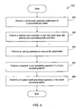
- FIG 4 illustrates a flowchart diagram 400 in accordance with another embodiment of the present invention.
- operations 302, 304, and 306 are again performed as described with reference to Figure 3 .
- the wafer is moved into a brush scrubbing station in order to perform a chemical brush scrubbing operation in 402.
- the brush scrubbing operation will preferably include the application of a combination of chemicals through the brush (TTB).
- the combination of chemicals will include H 2 O 2 , NH 4 OH, and de-ionized water, otherwise described as SC1.
- the preferred ratios by volume of H 2 O 2 :NH 4 OH:DI water are 10:1:120:, respectively.
- NH 4 OH is obtained as a stock solution that is about 29% NH 4 OH and the rest DI water.
- a stock solution of H 2 O 2 is typically about 30% H 2 O 2 and the rest DI water.
- NH 4 OH, and DI water will actually change accordingly when the concentrations of the stock solutions are taken into consideration.
- the chemical brush scrubbing of operation 402 will preferably have an optimal flow rate for H 2 O 2 , NH 4 OH, and DI water (e.g., SC1), and another separate flow rate for DI water.
- the brush scrubbing station will have a mix manifold that will receive a flow rate of about 250 ml/minute of H 2 O 2 , NH 4 OH, and DI water, and a flow rate of about 200 ml/minute of DI water. These two flows will thus be properly mixed in the mix manifold to dilute the chemical application to a desired level and thus apply the diluted chemical to the pair of brushes for through-the-brush scrubbing of the wafer.
- the optimal time for brush scrubbing in operation 402 will range between about 10 seconds and about 30 seconds, and most preferably, for about 20 seconds.
- the method will proceed to an operation 404 where a DI water brush scrubbing operation is performed in the same brush scrubbing station. In this operation, between about 2200 and about 3000 ml/minute is delivered to the brushes of the brush scrubbing station to perform a rinse that is configured to further remove any loose etch polymers and other residues.
- the DI water brush scrubbing operation 404 is also designed to flush out the chemicals from the chemical brush scrubbing operation 402 and thus ensure that the wafer is properly clean and is ready for the next fabrication operation. At this point, the method of this embodiment will end.
- FIG. 5 illustrates a flowchart diagram 500. Operations 302, 304, and 306 will be substantially the same as described with reference to Figures 3 and 4 above. The method now proceeds to an operation 502 where a hydrofluoric acid (HF) chemical brush scrubbing operation is performed in a brush scrubbing station in order to remove the generated etch polymers and any residues generated during the ashing operation.
- HF hydrofluoric acid
- the HF chemical will be a dilute HF chemical having a concentration ratio of 100:1. That is, for every 100 parts of DI water, there will be one part of HF.
- the stock solution of HF is typically comprised of about 49% pure HF by volume. Accordingly, the true concentration ratio of DI water to HF is actually about 100:0.5.
- the dilute HF solution is then provided to a mix manifold at about 250 ml/minute in addition to a flow of DI water of about 900 ml/minute.
- the flows of the dilute HF and the DI water will thus be mixed in a mix manifold before being applied to the brushes in the brush scrubbing station.
- the brush scrubbing operation will be performed for between about 20 seconds and about 40 seconds, and most preferably, for about 30 seconds.
- the HF chemical brush scrubbing operation will be performed with care such that the HF will not attack the underlying layers.
- the method will move to an operation 504 where a DI water brush scrubbing operation is performed in the brush scrubbing station.
- a DI water brush scrubbing operation is performed in the brush scrubbing station.
- between about 2200 and about 3000 ml/minute is passed to the brushes in the brush station to flush out any loose contaminants, particulates, as wells as any HF chemical solution from the brushes.
- This DI water brush scrubbing operation of 504 is thus configured to ensure that the surface of the wafer is left in a clean state before proceeding to further fabrication of other layers.
- FIG. 6 illustrates a flowchart diagram 600, in accordance with still another embodiment of the present invention.
- the method operations 302, 304, and 306 will be substantially the same as described above.
- a brush scrubbing system will include a first brush scrubbing station and a second brush scrubbing station.
- the brush scrubbing system may be similar to that described with reference to Figures 1B and 1C above, or two vertical brush scrubbers.
- a first chemical brush scrubbing operation is performed in a first brush scrubbing station.
- the stock solution of NH 4 OH is typically about 29% NH 4 OH and the stock solution for H 2 O 2 is typically about 30% H 2 O 2.
- the volumetric ratio 10:1:120 will be appropriately modified depending upon the stock solution used.
- the optimal flow for performing the first chemical brush scrubbing operation will be to apply about 250 ml per minute of SC1 (e.g., H 2 O 2 , NH 4 OH, DI water), and about 200 ml per minute of DI water by way of a mix manifold.
- SC1 e.g., H 2 O 2 , NH 4 OH, DI water
- This diluted solution is thus applied to the brushes to perform the first brush scrubbing operation in the first brush scrubbing station for a period of between about 10 seconds and about 30 seconds.
- the method will proceed to an operation 604 where a DI water brush scrubbing operation is performed in the same first brush scrubbing station.
- the brushes are flushed with a flow ranging between about 2200 and about 3000 ml per minute of DI water.
- a flow ranging between about 2200 and about 3000 ml per minute of DI water.
- the second chemical brush scrubbing operation will preferably include the application of a dilute HF chemical having a volumetric concentration ratio of about 100:1, where the stock HF solution is about 49% HF by volume.
- the dilute HF solution is applied at a flow rate of about 250 ml per minute, and is combined with a flow rate of DI water of about 900 ml per minute which is provided by way of a mix manifold.
- the mix manifold will then deliver the appropriately diluted HF solution to the brushes of the second brush scrubbing station for application to the wafer.
- the brush scrubbing operation will range in time between about 20 seconds and about 40 seconds, and most preferably for about 30 seconds.
- the method will proceed to an operation 608 where a DI water brush scrubbing operation is performed in the same second brush scrubbing station.
- This DI water brush scrubbing operation will be configured to deliver between about 2200 and about 300 ml/minute of DI water through the brush (TTB) to complete the cleaning of the wafer.
- the present invention can be modified to scrub any number of substrate types, for example, semiconductor wafers, flat panel displays, and the like. Additionally, the methods of the present invention are equally applicable to cleaning any size wafer, for example, 100 mm wafers, 200 mm wafers, 300 mm wafers, smaller wafers, larger wafers, etc.
Landscapes
- Cleaning Or Drying Semiconductors (AREA)
- Cleaning In General (AREA)
- Cleaning By Liquid Or Steam (AREA)
- Drying Of Semiconductors (AREA)
- Weting (AREA)
Abstract
Description
- This invention relates generally to substrate fabrication, and more particularly to semiconductor wafer cleaning after etch operations.
- As is well known, semiconductor devices are fabricated from semiconductor wafers, which are subjected to numerous processing operations. These operations include, for example, impurity implants, gate oxide generation, inter-metal oxide depositions, metallization depositions, photolithography pattering, etching operations, chemical mechanical polishing (CMP), etc.
- To facilitate discussion,
Figure 1 illustrates a cross-section view of a layer stack, representing the layers formed during the fabrication of a typical semiconductor integrated circuit (IC) device. It should be noted that additional layers above, below, or between the layers shown may be present. Further, not all of the illustrated layers need necessarily be present and some or all may be substituted by a variety of different layers. - At the bottom of the layer stack, there is shown a
substrate 10. Anoxide layer 11 which is typically a silicon dioxide (SiO2) is shown formed over the surface of thesubstrate 10. Abarrier layer 12, typically formed of Ti, TiW, TiN or other suitable barrier materials, may be disposed betweenoxide layer 11 and a subsequently depositedmetallization layer 13.Barrier layer 12, when provided, functions to substantially prevent diffusion of silicon atoms fromoxide layer 11 and into themetallization layer 13. -
Metallization layer 13 typically includes aluminum, copper or one or more of a variety of known aluminum alloys such as Al-Cu, Al-Si, and Al-Cu-Si. Also shown is an anti-reflective coating (ARC)layer 14 that is formed overmetallization layer 13. As is well known in the art,ARC layer 14 is typically composed of Ti, TiN or TiW. Generally speaking,ARC layer 14 is useful in preventing light used in photolithography processes from reflecting and scattering off of themetallization layer 13 surface. Anotheroxide layer 16 is then formed over theARC layer 14. In this simplified example, aphotoresist layer 18 is then spin coated over theoxide layer 16 and patterned to define windows where etching is desired. As is well known,photoresist layer 18 represents a layer of conventional photo-sensitive resist material that may be patterned using patterned reticles and a stepper that passes selective light waves onto the surface ofphotoresist layer 18. The layers of the layer stack are readily recognizable to those skilled in the art and may be formed using any number of known deposition processes, including chemical vapor deposition (CVD), plasma-enhanced chemical vapor deposition (PECVD), physical vapor deposition (PVD) such as sputtering, spin coating, etc. - At this point, an
etch operation 20 is performed in order to selectively remove portions of theoxide 16. In this example, afeature 17 is etched into theoxide 16, and thefeature 17 may be a trench, a via hole, or any other geometric pattern. Preferably, theetch 20 is chosen to have good selectivity to enable efficient etching of theoxide 16. During the etching operation, however,polymer formation 22 is known to occur on the sidewalls offeatures 17 being etched. Thispolymer formation 22, as shown, typically takes on the shape of a crown or a veil. This shape therefore is observed to extend along the sidewalls and up onto thephotoresist layer 18. - The actual composition of the
polymer formation 22 depends upon the material being etched, the chemistry used for the etching, and the underlying material (e.g., the ARC layer 14). Although there are many types of chemistries used to plasma etch through anoxide layer 16, typical chemistries may include CF4 and O2, NF3, and C4F8 among others. Thus, the material representing thepolymer formation 22 will generally be an oxide material containing some of the etch chemistry components, carbon from the photoresist, and metallization material (e.g., Ti, TiN, Al, Si, and Cu) from theARC layer 14 and themetal layer 13. - After the plasma etching is performed, the conventional process is to perform what is referred to as an ashing operation to remove the
photoresist layer 18. This ashing operation may remove some of thepolymer formation 22, however, most may still remain on the sidewalls of theetched oxide layer 16. To remove thisremaining polymer formation 22, it is conventional practice to move the wafer into a chemical bath containing liquids that are designed to remove thepolymer formation 22. An example chemical bath may include a chemical referred to as EKC-265, which is available from EKC, Inc. of Hayward, California. - Although chemical bath rinsing has worked in the past, the demand for smaller device features has increased the need to have a very clean environment at every step of a fabrication process. Unfortunately, bath rinsing is inherently an unclean environment. Polymer material being rinsed in the bath may therefore contaminate the bath, and the removed material may be deposited or can attach to other parts of a wafer or to other wafers being processed through the bath. In some cases, the
polymer formation 22 material may become lodged at the base of an etched feature, and due to its oxide composition, the material may prevent electrical contact through that feature (e.g., once a next metal formation step is performed to fill the oxide etched feature). Accordingly, surface particles and contaminants can detrimentally impact the performance of an integrated circuit device. - In view of the foregoing, there is a need for improved methods that will enable efficient removal of post plasma etch polymer materials from etched features. The removal should be efficient enough to remove the polymer material and prevent further contamination of other surface areas of a wafer being processed.
- Relevant background publications include: European Patent Application No.
0827188 A discloses a cleaning liquid for making a semiconductor device; SOLID STATE TECHNOLOGY, vol. 38, no. 6, 1 June 1995, (pages 109-110, 112, 114), which discloses the use of mechanical brushes to scrub the surface of semiconductor wafers; International Patent Application No.9713590 A - Broadly speaking, the present invention fills these needs by providing methods for efficiently cleaning etched features of given layers of a semiconductor wafer. Preferably the cleaning is designed to efficiently remove post plasma etch polymers from etched features. Several preferred embodiments of the present invention are described below.
- According to the present invention there is provided a method for cleaning a semiconductor wafer, the semiconductor wafer having an oxide layer, the oxide layer having a photoresist mask, the cleaning configured to remove polymer residues deposited during plasma etching a feature in the oxide layer using a photoresist mask that is removed by ashing, comprising:
- brush scrubbing the oxide layer of the semiconductor wafer and the plasma etched feature implementing chemicals delivered to a cleaning interface through the brush, the brush scrubbing configured to remove polymer residues deposited in and around the feature during the plasma etching wherein the chemicals are a combination of H2O2, NH4OH, and DI water having a ratio by volume of 10:1:120 and a flow rate of 250 ml/minute, wherein a stock solution of NH4OH is 29% NH4OH and a stock solution of H2O2 is 30% H2O2 wherein the combination of H2O2, NH4OH, and DI water is delivered to a mix manifold of a brush scrubbing station along with a delivery of a second DI water source at a flow rate of 200 ml/minute.
- Other aspects and advantages of the invention will become apparent from the following detailed description, taken in conjunction with the accompanying drawings, illustrating by way of example the principles of the invention.
- The present invention will be readily understood by the following detailed description in conjunction with the accompanying drawings, and like reference numerals designate like structural elements.
-
Figure 1A provides a diagram of a semiconductor wafer having layers formed thereon and an associated plasma etching operation. -
Figure 1B shows a wafer cleaning station on which the present invention can be implemented and that may be controlled in an automated way by a cleaning control station. -
Figure 1C shows a more detailed schematic of an exemplary wafer cleaning station. -
Figure 2A illustrates a simplified three-dimensional diagram of a pair of brushes scrubbing a top surface and a bottom surface of a wafer. -
Figures 2B and 2C illustrate cross-sectional views of two different orientations for scrubbing a wafer. -
Figure 3 illustrates a flowchart diagram defining the method operations performed when cleaning a semiconductor wafer after an etching operation has been performed, in accordance with one embodiment of the present invention. -
Figure 4 illustrates a flowchart diagram defining post plasma etch cleaning, in accordance with another embodiment of the present invention. -
Figure 5 illustrates a flowchart diagram defining post plasma etch cleaning. -
Figure 6 illustrates a flowchart diagram defining post plasma etch cleaning, in accordance with still another embodiment of the present invention. - An invention is described for methods of efficiently cleaning etched features of given layers of a semiconductor wafer. Preferably, the cleaning is designed to efficiently remove post plasma etch polymers and other particulates from in and around etched features. It will be obvious, however, to one skilled in the art, that the present invention may be practiced without some or all of these specific details. In other instances, well known process operations have not been described in detail in order not to unnecessarily obscure the present invention.
- The following description provided with reference to
Figures 1B through 2C will introduce exemplary preparation units and their respective orientations in which substrates can be processed. The flowcharts ofFigures 3 through 6 will then describe exemplary method operations that can be performed to clean wafers after etch operations. In one embodiment, the methods of the present invention enable efficient cleaning of polymers deposited during etching operations and other operations that may produce particulates or contaminants. -
Figure 1B shows awafer cleaning station 100 that may be controlled in an automated way by acleaning control station 102. Thewafer cleaning station 100 includes asender station 104, acleaning stage 106, a spin-rinse and dry (SRD)station 108, and areceiver station 110. It should be understood that cleaning systems can be used to carry out different kinds of substrate preparation operations, such as, cleaning, etching, buffing, and the like. With this in mind, as a broad overview of a cleaning process, semiconductor wafers are initially placed into thesender station 104. Thesender station 104 then delivers wafers (one-at-a-time) to thecleaning stage 106. In one embodiment, thecleaning stage 106 is divided into afirst cleaning stage 106a and asecond cleaning stage 106b, although having just onecleaning stage 106 will also work. After passing through thecleaning stage 106, the wafer is passed through an exit spray in order to remove the cleaning fluids and any contaminants. TheSRD station 108 dries the wafer and then it is delivered to thereceiver station 110 for temporary storage. -
Figure 1C shows a more detailed schematic of an exemplarywafer cleaning station 100. Both thesender station 104 and the receivingstation 110 are preferably adapted to receive a cassette containing a number of wafers. The first andsecond cleaning stages brushes 120 are capable of scrubbing the wafer without damaging the delicate surface. -
Figure 2A illustrates a simplified three-dimensional diagram of a pair ofbrushes wafer 130. Typically, thewafer 130 is caused to rotate in a particular direction while thebrushes 120 rotate around an axis of rotation and the surface of thebrushes 120 are in contact with the surfaces of thewafer 130. Thebrushes brush cores shaft 201 which has a fluid inlet 202. The fluid inlet 202 will thus supply the desired fluids into the brush cores 200. The brush cores 200 preferably have a plurality of holes that will allow the fluids to uniformly exit the brush core 200 and evenly supply the desired fluid to thebrush 120. -
Figures 2B and 2C illustrate cross-sectional views of two different orientations for scrubbing awafer 130. As shown inFigure 2B , the wafer is held horizontally while atop brush 120a scrubs the top surface of thewafer 130, and abottom brush 120b scrubs the bottom surface of thewafer 130. As mentioned above, thewafer 130 is configured to rotate (using rollers not shown) at the same time that thebrushes 120 rotate to ensure that the entire surface area of the wafer is properly scrubbed to remove contaminants, etch the surface to a desired degree, or buff the surface. Thus,Figure 2B illustrates ahorizontal wafer scrubber 100b. - In contrast,
Figure 2C illustrates avertical wafer scrubber 100c in which thewafer 130 is scrubbed while in a vertical position. Typically, thewafer 130 sits on a pair of rollers of thescrubber 100c. Thebrushes 120 are configured to rotate in a desired direction such that both sides of thewafer 130 are evenly scrubbed, using an equal and opposite pressure on each side of thewafer 130. For more information on vertical wafer scrubbing, reference may be made toU.S. Pat. No. 5,875,507 , having inventors Stephens et al., entitled "Wafer Cleaning Apparatus,". -
Figure 3 illustrates a flowchart diagram 300 defining the method operations performed when cleaning a semiconductor wafer after an etching operation has been performed, in accordance with one embodiment of the present invention. The method begins at anoperation 302 where a photoresist patterned oxide layer of a semiconductor wafer is provided. As shown inFigure 1 , a semiconductor wafer may have a plurality of layers fabrication thereon, and the photoresist layer is used to pattern a desired layer. In this example, in the layer requiring patterning is an oxide layer. As is well known, oxide layers are typically inorganic or organic dielectric materials which are used to insulate interconnect metallization lines between interconnect levels. The method now moves to anoperation 304 where a plasma etch operation is performed to etch the oxide layer using the patterned photoresist to define etched feature regions. In one embodiment, the plasma etching may be used to perform via hole etching, contact hole etching, trenches, and other features in the oxide layer. - The plasma etch operation will typically generate a layer of polymers on the sidewalls of the etched features. The formed polymers are known to be a composition of the plasma etching chemistries, carbon from photoresist material, the oxide material being etched, and components from the material that underlies the oxide layer being etched. For example, the underlying layer may be some type of metallization layer, such as an antireflective coating (ARC).
- To remove the patterned photoresist from over the patterned oxide layer, the method will move to an
operation 306 where an ashing operation is performed. Ashing operations are well known and are commonly used to remove photoresist materials. When the ashing operation is complete and the photoresist material has been removed, the wafer will be processed through a brush scrubbing system in order to remove the generated etch polymers and any ashing residues inoperation 308. For example, the brush scrubbing operation can be performed in a brush scrubbing station that incorporates a pair of brushes for evenly brushing each side of the processed semiconductor wafer. - In a preferred embodiment, the brush scrubbing operation will preferably implement a chemical that will assist in removing the generated etched polymers, any of the ashing residues, and other particulates or contaminants. For example, the brushing operation is designed to be performed by supplying chemicals through the brush (TTB) to allow the scrubbing of the surface for a period of between about 10 seconds and about 40 seconds. It should be noted that brush scrub cleaning in the context of post etch and ashing operations is substantially different that the conventional technique of chemical bath treatment, which is known to further contaminate a wafer with particulates.
- Exemplary chemicals may include: (a) a combination of ammonia (NH4OH) and de-ionized (DI) water, (b) a combination of peroxide (H2O2), hydrofluoric acid (HF), and DI water, (c) a combination of peroxide (H2O2), ammonia (NH4OH), and DI water, and (d) a combination of HF and DI water. Combination (c) of H2O2, NH4OH, and DI water is referred to as "SC1." For additional information on wafer cleaning processes, reference may be made to this commonly owned
U.S. patent application number 08/792,093, filed January 31, 1997 - Once the chemical application and scrubbing has been performed for the desired amount of time, the method will conclude by performing a DI water rinse through the brush in the same brush scrubbing station. It should be understood that the brush scrubbing operation that includes the delivery of chemicals followed by a DI water rinse is configured to yield a high degree of cleanliness while removing the generated etch polymers from within the etched oxide features, as well as removing other particulates and contaminants that may have been deposited during the ashing operation. Accordingly, the method of the present invention enables a very simple cleaning operation to be performed as a post-etch treatment that follows an ashing operation. Once the
brush scrubbing operation 308 is performed, the wafer can be moved to further processing and the method will end. -
Figure 4 illustrates a flowchart diagram 400 in accordance with another embodiment of the present invention. In this embodiment,operations Figure 3 . Once the wafer has been processed through the ashing operation to remove the photoresist inoperation 306, the wafer is moved into a brush scrubbing station in order to perform a chemical brush scrubbing operation in 402. The brush scrubbing operation will preferably include the application of a combination of chemicals through the brush (TTB). - For example, the combination of chemicals will include H2O2, NH4OH, and de-ionized water, otherwise described as SC1. The preferred ratios by volume of H2O2:NH4OH:DI water are 10:1:120:, respectively. Typically, NH4OH is obtained as a stock solution that is about 29% NH4OH and the rest DI water. Similarly, a stock solution of H2O2 is typically about 30% H2O2 and the rest DI water. Thus, the volumetric ratio of 10:1:120 for H2O2. NH4OH, and DI water will actually change accordingly when the concentrations of the stock solutions are taken into consideration.
- In operation, the chemical brush scrubbing of
operation 402 will preferably have an optimal flow rate for H2O2, NH4OH, and DI water (e.g., SC1), and another separate flow rate for DI water. Preferably, the brush scrubbing station will have a mix manifold that will receive a flow rate of about 250 ml/minute of H2O2, NH4OH, and DI water, and a flow rate of about 200 ml/minute of DI water. These two flows will thus be properly mixed in the mix manifold to dilute the chemical application to a desired level and thus apply the diluted chemical to the pair of brushes for through-the-brush scrubbing of the wafer. - In one embodiment, the optimal time for brush scrubbing in
operation 402 will range between about 10 seconds and about 30 seconds, and most preferably, for about 20 seconds. Once the chemical brush scrubbing operation is complete inoperation 402, the method will proceed to anoperation 404 where a DI water brush scrubbing operation is performed in the same brush scrubbing station. In this operation, between about 2200 and about 3000 ml/minute is delivered to the brushes of the brush scrubbing station to perform a rinse that is configured to further remove any loose etch polymers and other residues. The DI waterbrush scrubbing operation 404 is also designed to flush out the chemicals from the chemicalbrush scrubbing operation 402 and thus ensure that the wafer is properly clean and is ready for the next fabrication operation. At this point, the method of this embodiment will end. -
Figure 5 illustrates a flowchart diagram 500.Operations Figures 3 and4 above. The method now proceeds to anoperation 502 where a hydrofluoric acid (HF) chemical brush scrubbing operation is performed in a brush scrubbing station in order to remove the generated etch polymers and any residues generated during the ashing operation. - In this embodiment, the HF chemical will be a dilute HF chemical having a concentration ratio of 100:1. That is, for every 100 parts of DI water, there will be one part of HF. However, the stock solution of HF is typically comprised of about 49% pure HF by volume. Accordingly, the true concentration ratio of DI water to HF is actually about 100:0.5. In operation, the dilute HF solution is then provided to a mix manifold at about 250 ml/minute in addition to a flow of DI water of about 900 ml/minute. The flows of the dilute HF and the DI water will thus be mixed in a mix manifold before being applied to the brushes in the brush scrubbing station. In a preferred embodiment, the brush scrubbing operation will be performed for between about 20 seconds and about 40 seconds, and most preferably, for about 30 seconds.
- In general, the HF chemical brush scrubbing operation will be performed with care such that the HF will not attack the underlying layers. Once the HF brush scrubbing operation is performed in
operation 502, the method will move to anoperation 504 where a DI water brush scrubbing operation is performed in the brush scrubbing station. In this embodiment, between about 2200 and about 3000 ml/minute is passed to the brushes in the brush station to flush out any loose contaminants, particulates, as wells as any HF chemical solution from the brushes. This DI water brush scrubbing operation of 504 is thus configured to ensure that the surface of the wafer is left in a clean state before proceeding to further fabrication of other layers. -
Figure 6 illustrates a flowchart diagram 600, in accordance with still another embodiment of the present invention. In this embodiment, themethod operations Figures 1B and1C above, or two vertical brush scrubbers. - Accordingly, method proceeds to an
operation 602 where a first chemical brush scrubbing operation is performed in a first brush scrubbing station. In this first chemical brush scrubbing operation, it is preferred that a chemical including H2O2, NH4OH, and DI water (e.g., SC1) having a volumetric ratio of 10:1:120, respectively, be used through the brush (TTB) during the scrub operation. As mentioned above, the stock solution of NH4OH is typically about 29% NH4OH and the stock solution for H2O2 is typically about 30% H2O2. Thus, the volumetric ratio 10:1:120 will be appropriately modified depending upon the stock solution used. - In any event, the optimal flow for performing the first chemical brush scrubbing operation will be to apply about 250 ml per minute of SC1 (e.g., H2O2, NH4OH, DI water), and about 200 ml per minute of DI water by way of a mix manifold. This diluted solution is thus applied to the brushes to perform the first brush scrubbing operation in the first brush scrubbing station for a period of between about 10 seconds and about 30 seconds. Once the first chemical brush scrubbing operation is performed in
operation 602, the method will proceed to anoperation 604 where a DI water brush scrubbing operation is performed in the same first brush scrubbing station. Preferably, the brushes are flushed with a flow ranging between about 2200 and about 3000 ml per minute of DI water. Once the DI water brush scrubbing operation is complete inoperation 604, the method will proceed to anoperation 606 where a second chemical brush scrubbing operation is performed in a second brush scrubbing station. - Accordingly, the wafer will have to be moved between the first brush scrubbing station and the second brush scrubbing station in order to perform the second chemical brush scrubbing operation. The second chemical brush scrubbing operation will preferably include the application of a dilute HF chemical having a volumetric concentration ratio of about 100:1, where the stock HF solution is about 49% HF by volume. Preferably, the dilute HF solution is applied at a flow rate of about 250 ml per minute, and is combined with a flow rate of DI water of about 900 ml per minute which is provided by way of a mix manifold. The mix manifold will then deliver the appropriately diluted HF solution to the brushes of the second brush scrubbing station for application to the wafer. Preferably, the brush scrubbing operation will range in time between about 20 seconds and about 40 seconds, and most preferably for about 30 seconds.
- Once the second chemical brush scrubbing operation is complete in
operation 606, the method will proceed to anoperation 608 where a DI water brush scrubbing operation is performed in the same second brush scrubbing station. This DI water brush scrubbing operation will be configured to deliver between about 2200 and about 300 ml/minute of DI water through the brush (TTB) to complete the cleaning of the wafer. - It is again noted that the present invention can be modified to scrub any number of substrate types, for example, semiconductor wafers, flat panel displays, and the like. Additionally, the methods of the present invention are equally applicable to cleaning any size wafer, for example, 100 mm wafers, 200 mm wafers, 300 mm wafers, smaller wafers, larger wafers, etc.
- For additional information on wafer preparing systems and techniques, reference may be made to commonly owned U.S. patent application numbers: (1)
08/542,531, filed October 13, 1995 , entitled "Method and Apparatus for Chemical Delivery Through the Brush," and (2)09/277,712, filed March 26, 1999
Claims (6)
- A method for cleaning a semiconductor wafer, the semiconductor waferhaving an oxide layer, the oxide layer having a photoresist mask, the cleaning configured to remove polymer residues deposited during plasma etching a feature in the oxide layer using a photoresist mask that is removed by ashing, comprising:brush scrubbing the oxide layer of the semiconductor wafer and the plasma etched feature implementing chemicals delivered to a cleaning interface through the brush, the brush scrubbing configured to remove polymer residues deposited in and around the feature during the plasma etching wherein the chemicals are a combination of H2O2, NH4OH, and DI water having a ratio by volume of 10:1:120 and a flow rate of 250 ml/minute, wherein a stock solution of NH4OH is 29% NH4OH and a stock solution of H2O2 is 30% H2O2 wherein the combination of H2O2, NH4OH, and DI water is delivered to a mix manifold of a brush scrubbing station along with a delivery of a second DI water source at a flow rate of 200 ml/minute and wherein the mix manifold being configured to deliver a chemical fluid to brushes of the brush scrubbing station to perform the brush scrubbing of the semiconductor wafer.
- A method for cleaning a semiconductor wafer as recited in claim 1, wherein the brush scrubbing is performed for a time ranging between 10 seconds and 30 seconds.
- A method for cleaning a semiconductor wafer as recited in claim 2, further comprising:brush scrubbing the semiconductor wafer with a DI water rinse following the brush scrubbing with the chemicals.
- A method for cleaning a semiconductor wafer as recited in claim 3, further comprising:performing a second brush scrubbing operation on the oxide layer and the plasma etched feature with second chemicals followed by a second DI water rinse, the second chemicals being a combination of HF and DI water.
- A method for cleaning a semiconductor wafer as recited in claim 4, wherein the second brush scrubbing with the HF and DI water is performed for a period of time ranging between 20 seconds and 40 seconds.
- A method for cleaning a semiconductor wafer as recited in claim 5, wherein the HF and DI water has a concentration ratio of 1:100 wherein the HF and DI water is delivered to a mix manifold of a brush scrubbing station at a flow rate of 250 ml/minute along with a delivery of a second DI water source at a flow rate of 900 ml/minute, the mix manifold being configured to deliver a chemical fluid to brushes of the brush scrubbing station to perform the second brush scrubbing of the semiconductor wafer, and wherein the HF is a stock solution of 49% HF and 51% DI water.
Applications Claiming Priority (2)
| Application Number | Priority Date | Filing Date | Title |
|---|---|---|---|
| US458550 | 1999-12-09 | ||
| US09/458,550 US6187684B1 (en) | 1999-12-09 | 1999-12-09 | Methods for cleaning substrate surfaces after etch operations |
Publications (3)
| Publication Number | Publication Date |
|---|---|
| EP1107301A2 EP1107301A2 (en) | 2001-06-13 |
| EP1107301A3 EP1107301A3 (en) | 2002-03-06 |
| EP1107301B1 true EP1107301B1 (en) | 2010-01-13 |
Family
ID=23821214
Family Applications (1)
| Application Number | Title | Priority Date | Filing Date |
|---|---|---|---|
| EP00310491A Expired - Lifetime EP1107301B1 (en) | 1999-12-09 | 2000-11-27 | Methods for cleaning substrate surfaces after etch operations |
Country Status (6)
| Country | Link |
|---|---|
| US (1) | US6187684B1 (en) |
| EP (1) | EP1107301B1 (en) |
| JP (1) | JP4891475B2 (en) |
| AT (1) | ATE455368T1 (en) |
| DE (1) | DE60043686D1 (en) |
| TW (1) | TW499719B (en) |
Families Citing this family (35)
| Publication number | Priority date | Publication date | Assignee | Title |
|---|---|---|---|---|
| EP1077474A3 (en) | 1999-08-14 | 2004-05-12 | Applied Materials, Inc. | Backside etching in a scrubber |
| US6432618B1 (en) * | 2000-02-11 | 2002-08-13 | Advanced Micro Devices, Inc. | Method for forming high quality multiple thickness oxide layers by reducing descum induced defects |
| US6416391B1 (en) * | 2000-02-28 | 2002-07-09 | Seh America, Inc. | Method of demounting silicon wafers after polishing |
| WO2002054458A2 (en) * | 2001-01-08 | 2002-07-11 | International Business Machines Corporation | Method for the manufacture of micro structures |
| TW525402B (en) | 2001-01-18 | 2003-03-21 | Semiconductor Energy Lab | Process for producing a light emitting device |
| SG143944A1 (en) * | 2001-02-19 | 2008-07-29 | Semiconductor Energy Lab | Light emitting device and method of manufacturing the same |
| US6720198B2 (en) * | 2001-02-19 | 2004-04-13 | Semiconductor Energy Laboratory Co., Ltd. | Light emitting device and manufacturing method thereof |
| US6951823B2 (en) * | 2001-05-14 | 2005-10-04 | Axcelis Technologies, Inc. | Plasma ashing process |
| US20030011018A1 (en) * | 2001-07-13 | 2003-01-16 | Hurley Kelly T. | Flash floating gate using epitaxial overgrowth |
| US6676493B1 (en) | 2001-12-26 | 2004-01-13 | Lam Research Corporation | Integrated planarization and clean wafer processing system |
| US6949411B1 (en) | 2001-12-27 | 2005-09-27 | Lam Research Corporation | Method for post-etch and strip residue removal on coral films |
| US20030235998A1 (en) * | 2002-06-24 | 2003-12-25 | Ming-Chung Liang | Method for eliminating standing waves in a photoresist profile |
| SG130013A1 (en) * | 2002-07-25 | 2007-03-20 | Semiconductor Energy Lab | Method of fabricating light emitting device |
| US7066789B2 (en) * | 2002-07-29 | 2006-06-27 | Manoclean Technologies, Inc. | Methods for resist stripping and other processes for cleaning surfaces substantially free of contaminants |
| US6764385B2 (en) * | 2002-07-29 | 2004-07-20 | Nanoclean Technologies, Inc. | Methods for resist stripping and cleaning surfaces substantially free of contaminants |
| US7297286B2 (en) * | 2002-07-29 | 2007-11-20 | Nanoclean Technologies, Inc. | Methods for resist stripping and other processes for cleaning surfaces substantially free of contaminants |
| US7101260B2 (en) * | 2002-07-29 | 2006-09-05 | Nanoclean Technologies, Inc. | Methods for resist stripping and other processes for cleaning surfaces substantially free of contaminants |
| US7134941B2 (en) * | 2002-07-29 | 2006-11-14 | Nanoclean Technologies, Inc. | Methods for residue removal and corrosion prevention in a post-metal etch process |
| AU2003260959A1 (en) * | 2002-09-11 | 2004-04-30 | Semiconductor Energy Laboratory Co., Ltd. | Light-emitting apparatus and fabrication method of the same |
| US7224035B1 (en) * | 2002-10-07 | 2007-05-29 | Zyvex Corporation | Apparatus and fabrication methods for incorporating sub-millimeter, high-resistivity mechanical components with low-resistivity conductors while maintaining electrical isolation therebetween |
| JP2004165241A (en) * | 2002-11-11 | 2004-06-10 | Sanyo Electric Co Ltd | Semiconductor device and manufacturing method thereof |
| JP2004259882A (en) * | 2003-02-25 | 2004-09-16 | Seiko Epson Corp | Semiconductor device and manufacturing method thereof |
| US6936544B2 (en) * | 2003-03-11 | 2005-08-30 | Taiwan Semiconductor Manufacturing Co., Ltd. | Method of removing metal etching residues following a metal etchback process to improve a CMP process |
| US20040256354A1 (en) * | 2003-06-18 | 2004-12-23 | Raluca Dinu | Method of removing etch veils from microstructures |
| US20050011535A1 (en) * | 2003-07-18 | 2005-01-20 | Randy Skocypec | Cleaning semiconductor wafers |
| KR100562302B1 (en) * | 2003-12-27 | 2006-03-22 | 동부아남반도체 주식회사 | Random Polymer Removal Using Multi-Chemical Liquid Treatment Steps |
| US20050252547A1 (en) * | 2004-05-11 | 2005-11-17 | Applied Materials, Inc. | Methods and apparatus for liquid chemical delivery |
| KR100672664B1 (en) * | 2004-12-29 | 2007-01-24 | 동부일렉트로닉스 주식회사 | Manufacturing method of vertical CMOS image sensor |
| KR100606906B1 (en) * | 2004-12-29 | 2006-08-01 | 동부일렉트로닉스 주식회사 | Photodiode of CMOS image sensor and its manufacturing method |
| KR100660319B1 (en) * | 2004-12-30 | 2006-12-22 | 동부일렉트로닉스 주식회사 | CMOS image sensor and manufacturing method |
| US7535031B2 (en) * | 2005-09-13 | 2009-05-19 | Philips Lumiled Lighting, Co. Llc | Semiconductor light emitting device with lateral current injection in the light emitting region |
| TW201442122A (en) * | 2012-12-25 | 2014-11-01 | Ps4 Luxco Sarl | Semiconductor device manufacturing method |
| US9048268B2 (en) | 2013-03-05 | 2015-06-02 | Taiwan Semiconductor Manufacturing Co., Ltd. | Method and equipment for removing photoresist residue after dry etch |
| JP6975937B2 (en) * | 2017-09-28 | 2021-12-01 | パナソニックIpマネジメント株式会社 | Device chip manufacturing method and equipment |
| KR102573572B1 (en) * | 2017-12-20 | 2023-09-01 | 삼성전자주식회사 | Wafer cleaning apparatus |
Family Cites Families (9)
| Publication number | Priority date | Publication date | Assignee | Title |
|---|---|---|---|---|
| JPH06177089A (en) * | 1992-12-04 | 1994-06-24 | Fujitsu Ltd | Method for manufacturing semiconductor device |
| JP3353462B2 (en) * | 1994-06-10 | 2002-12-03 | ソニー株式会社 | Dry etching method |
| JPH08274077A (en) * | 1995-03-31 | 1996-10-18 | Sony Corp | Plasma etching method |
| JP3353532B2 (en) * | 1995-04-13 | 2002-12-03 | ソニー株式会社 | Trench etching method |
| WO1997013590A1 (en) * | 1995-10-13 | 1997-04-17 | Ontrak Systems, Inc. | Method and apparatus for chemical delivery through the brush |
| US6004839A (en) * | 1996-01-17 | 1999-12-21 | Nec Corporation | Semiconductor device with conductive plugs |
| DE19631363C1 (en) * | 1996-08-02 | 1998-02-12 | Siemens Ag | Aqueous cleaning solution for a semiconductor substrate |
| JPH1055993A (en) * | 1996-08-09 | 1998-02-24 | Hitachi Ltd | Cleaning solution for manufacturing semiconductor device and method for manufacturing semiconductor device using the same |
| US6024106A (en) * | 1998-11-19 | 2000-02-15 | United Microelectronics Corp. | Post-CMP wafer clean process |
-
1999
- 1999-12-09 US US09/458,550 patent/US6187684B1/en not_active Expired - Lifetime
-
2000
- 2000-11-27 EP EP00310491A patent/EP1107301B1/en not_active Expired - Lifetime
- 2000-11-27 AT AT00310491T patent/ATE455368T1/en not_active IP Right Cessation
- 2000-11-27 DE DE60043686T patent/DE60043686D1/en not_active Expired - Lifetime
- 2000-12-05 JP JP2000369826A patent/JP4891475B2/en not_active Expired - Fee Related
- 2000-12-06 TW TW089126038A patent/TW499719B/en not_active IP Right Cessation
Non-Patent Citations (1)
| Title |
|---|
| ELECTROCHEMICAL SOCIETY PROCEEDINGS, OCTOBER 1995, vol. 95, no. 20, 1996, PENNINGTON, NJ, USA, pages 409 - 420, XP001038630 * |
Also Published As
| Publication number | Publication date |
|---|---|
| TW499719B (en) | 2002-08-21 |
| DE60043686D1 (en) | 2010-03-04 |
| JP4891475B2 (en) | 2012-03-07 |
| EP1107301A2 (en) | 2001-06-13 |
| ATE455368T1 (en) | 2010-01-15 |
| EP1107301A3 (en) | 2002-03-06 |
| US6187684B1 (en) | 2001-02-13 |
| JP2001237236A (en) | 2001-08-31 |
Similar Documents
| Publication | Publication Date | Title |
|---|---|---|
| US6187684B1 (en) | Methods for cleaning substrate surfaces after etch operations | |
| US5858109A (en) | Method and apparatus for cleaning of semiconductor substrates using standard clean 1 (SC1) | |
| US7469883B2 (en) | Cleaning method and solution for cleaning a wafer in a single wafer process | |
| US5849639A (en) | Method for removing etching residues and contaminants | |
| KR101376897B1 (en) | Post etch wafer surface cleaning with liquid meniscus | |
| KR100554053B1 (en) | Semiconductor device and manufacturing method thereof | |
| US6277203B1 (en) | Method and apparatus for cleaning low K dielectric and metal wafer surfaces | |
| US6921494B2 (en) | Backside etching in a scrubber | |
| US20040074526A1 (en) | Method of manufacturing semiconductor device and apparatus for cleaning substrate | |
| EP0959490A2 (en) | A semiconductor device washing apparatus and a method of washing a semiconductordevice | |
| EP1459363B1 (en) | Method for post-etch and strip residue removal on coral films | |
| JP5470746B2 (en) | Manufacturing method of semiconductor device | |
| US7067015B2 (en) | Modified clean chemistry and megasonic nozzle for removing backside CMP slurries | |
| US8375965B2 (en) | Systems and methods for single integrated substrate cleaning and rinsing | |
| JP3421887B2 (en) | Cleaning method and cleaning device used therefor | |
| KR100600530B1 (en) | Method of Cleaning Semiconductor Devices | |
| CN119943645A (en) | Method for cleaning wafer |
Legal Events
| Date | Code | Title | Description |
|---|---|---|---|
| PUAI | Public reference made under article 153(3) epc to a published international application that has entered the european phase |
Free format text: ORIGINAL CODE: 0009012 |
|
| AK | Designated contracting states |
Kind code of ref document: A2 Designated state(s): AT BE CH CY DE DK ES FI FR GB GR IE IT LI LU MC NL PT SE TR |
|
| AX | Request for extension of the european patent |
Free format text: AL;LT;LV;MK;RO;SI |
|
| PUAL | Search report despatched |
Free format text: ORIGINAL CODE: 0009013 |
|
| AK | Designated contracting states |
Kind code of ref document: A3 Designated state(s): AT BE CH CY DE DK ES FI FR GB GR IE IT LI LU MC NL PT SE TR |
|
| AX | Request for extension of the european patent |
Free format text: AL;LT;LV;MK;RO;SI |
|
| RIC1 | Information provided on ipc code assigned before grant |
Free format text: 7H 01L 21/306 A, 7B 08B 1/04 B |
|
| 17P | Request for examination filed |
Effective date: 20020904 |
|
| AKX | Designation fees paid |
Free format text: AT BE CH CY DE DK ES FI FR GB GR IE IT LI LU MC NL PT SE TR |
|
| 17Q | First examination report despatched |
Effective date: 20021030 |
|
| 17Q | First examination report despatched |
Effective date: 20021030 |
|
| GRAP | Despatch of communication of intention to grant a patent |
Free format text: ORIGINAL CODE: EPIDOSNIGR1 |
|
| GRAJ | Information related to disapproval of communication of intention to grant by the applicant or resumption of examination proceedings by the epo deleted |
Free format text: ORIGINAL CODE: EPIDOSDIGR1 |
|
| GRAP | Despatch of communication of intention to grant a patent |
Free format text: ORIGINAL CODE: EPIDOSNIGR1 |
|
| GRAS | Grant fee paid |
Free format text: ORIGINAL CODE: EPIDOSNIGR3 |
|
| GRAA | (expected) grant |
Free format text: ORIGINAL CODE: 0009210 |
|
| AK | Designated contracting states |
Kind code of ref document: B1 Designated state(s): AT BE CH CY DE DK ES FI FR GB GR IE IT LI LU MC NL PT SE TR |
|
| REG | Reference to a national code |
Ref country code: GB Ref legal event code: FG4D |
|
| REG | Reference to a national code |
Ref country code: CH Ref legal event code: EP |
|
| REG | Reference to a national code |
Ref country code: IE Ref legal event code: FG4D |
|
| REF | Corresponds to: |
Ref document number: 60043686 Country of ref document: DE Date of ref document: 20100304 Kind code of ref document: P |
|
| REG | Reference to a national code |
Ref country code: NL Ref legal event code: VDEP Effective date: 20100113 |
|
| PG25 | Lapsed in a contracting state [announced via postgrant information from national office to epo] |
Ref country code: AT Free format text: LAPSE BECAUSE OF FAILURE TO SUBMIT A TRANSLATION OF THE DESCRIPTION OR TO PAY THE FEE WITHIN THE PRESCRIBED TIME-LIMIT Effective date: 20100113 |
|
| PG25 | Lapsed in a contracting state [announced via postgrant information from national office to epo] |
Ref country code: ES Free format text: LAPSE BECAUSE OF FAILURE TO SUBMIT A TRANSLATION OF THE DESCRIPTION OR TO PAY THE FEE WITHIN THE PRESCRIBED TIME-LIMIT Effective date: 20100424 Ref country code: PT Free format text: LAPSE BECAUSE OF FAILURE TO SUBMIT A TRANSLATION OF THE DESCRIPTION OR TO PAY THE FEE WITHIN THE PRESCRIBED TIME-LIMIT Effective date: 20100513 Ref country code: NL Free format text: LAPSE BECAUSE OF FAILURE TO SUBMIT A TRANSLATION OF THE DESCRIPTION OR TO PAY THE FEE WITHIN THE PRESCRIBED TIME-LIMIT Effective date: 20100113 |
|
| PG25 | Lapsed in a contracting state [announced via postgrant information from national office to epo] |
Ref country code: FI Free format text: LAPSE BECAUSE OF FAILURE TO SUBMIT A TRANSLATION OF THE DESCRIPTION OR TO PAY THE FEE WITHIN THE PRESCRIBED TIME-LIMIT Effective date: 20100113 |
|
| PG25 | Lapsed in a contracting state [announced via postgrant information from national office to epo] |
Ref country code: CY Free format text: LAPSE BECAUSE OF FAILURE TO SUBMIT A TRANSLATION OF THE DESCRIPTION OR TO PAY THE FEE WITHIN THE PRESCRIBED TIME-LIMIT Effective date: 20100113 Ref country code: BE Free format text: LAPSE BECAUSE OF FAILURE TO SUBMIT A TRANSLATION OF THE DESCRIPTION OR TO PAY THE FEE WITHIN THE PRESCRIBED TIME-LIMIT Effective date: 20100113 Ref country code: GR Free format text: LAPSE BECAUSE OF FAILURE TO SUBMIT A TRANSLATION OF THE DESCRIPTION OR TO PAY THE FEE WITHIN THE PRESCRIBED TIME-LIMIT Effective date: 20100414 Ref country code: SE Free format text: LAPSE BECAUSE OF FAILURE TO SUBMIT A TRANSLATION OF THE DESCRIPTION OR TO PAY THE FEE WITHIN THE PRESCRIBED TIME-LIMIT Effective date: 20100113 |
|
| PLBE | No opposition filed within time limit |
Free format text: ORIGINAL CODE: 0009261 |
|
| STAA | Information on the status of an ep patent application or granted ep patent |
Free format text: STATUS: NO OPPOSITION FILED WITHIN TIME LIMIT |
|
| 26N | No opposition filed |
Effective date: 20101014 |
|
| PG25 | Lapsed in a contracting state [announced via postgrant information from national office to epo] |
Ref country code: DK Free format text: LAPSE BECAUSE OF FAILURE TO SUBMIT A TRANSLATION OF THE DESCRIPTION OR TO PAY THE FEE WITHIN THE PRESCRIBED TIME-LIMIT Effective date: 20100113 |
|
| PG25 | Lapsed in a contracting state [announced via postgrant information from national office to epo] |
Ref country code: IT Free format text: LAPSE BECAUSE OF FAILURE TO SUBMIT A TRANSLATION OF THE DESCRIPTION OR TO PAY THE FEE WITHIN THE PRESCRIBED TIME-LIMIT Effective date: 20100113 |
|
| PG25 | Lapsed in a contracting state [announced via postgrant information from national office to epo] |
Ref country code: MC Free format text: LAPSE BECAUSE OF NON-PAYMENT OF DUE FEES Effective date: 20101130 |
|
| REG | Reference to a national code |
Ref country code: CH Ref legal event code: PL |
|
| GBPC | Gb: european patent ceased through non-payment of renewal fee |
Effective date: 20101127 |
|
| PG25 | Lapsed in a contracting state [announced via postgrant information from national office to epo] |
Ref country code: CH Free format text: LAPSE BECAUSE OF NON-PAYMENT OF DUE FEES Effective date: 20101130 Ref country code: LI Free format text: LAPSE BECAUSE OF NON-PAYMENT OF DUE FEES Effective date: 20101130 |
|
| REG | Reference to a national code |
Ref country code: FR Ref legal event code: ST Effective date: 20110801 |
|
| REG | Reference to a national code |
Ref country code: DE Ref legal event code: R119 Ref document number: 60043686 Country of ref document: DE Effective date: 20110601 Ref country code: DE Ref legal event code: R119 Ref document number: 60043686 Country of ref document: DE Effective date: 20110531 |
|
| PG25 | Lapsed in a contracting state [announced via postgrant information from national office to epo] |
Ref country code: DE Free format text: LAPSE BECAUSE OF NON-PAYMENT OF DUE FEES Effective date: 20110531 |
|
| PG25 | Lapsed in a contracting state [announced via postgrant information from national office to epo] |
Ref country code: FR Free format text: LAPSE BECAUSE OF NON-PAYMENT OF DUE FEES Effective date: 20101130 Ref country code: IE Free format text: LAPSE BECAUSE OF NON-PAYMENT OF DUE FEES Effective date: 20101127 |
|
| PG25 | Lapsed in a contracting state [announced via postgrant information from national office to epo] |
Ref country code: GB Free format text: LAPSE BECAUSE OF NON-PAYMENT OF DUE FEES Effective date: 20101127 |
|
| PG25 | Lapsed in a contracting state [announced via postgrant information from national office to epo] |
Ref country code: LU Free format text: LAPSE BECAUSE OF NON-PAYMENT OF DUE FEES Effective date: 20101127 |
|
| PG25 | Lapsed in a contracting state [announced via postgrant information from national office to epo] |
Ref country code: TR Free format text: LAPSE BECAUSE OF FAILURE TO SUBMIT A TRANSLATION OF THE DESCRIPTION OR TO PAY THE FEE WITHIN THE PRESCRIBED TIME-LIMIT Effective date: 20100113 |