EP1104949A2 - Coordinated switching in a multiple switching regulator system to lower peak current load - Google Patents
Coordinated switching in a multiple switching regulator system to lower peak current load Download PDFInfo
- Publication number
- EP1104949A2 EP1104949A2 EP00309850A EP00309850A EP1104949A2 EP 1104949 A2 EP1104949 A2 EP 1104949A2 EP 00309850 A EP00309850 A EP 00309850A EP 00309850 A EP00309850 A EP 00309850A EP 1104949 A2 EP1104949 A2 EP 1104949A2
- Authority
- EP
- European Patent Office
- Prior art keywords
- regulator
- switching
- switching regulator
- power source
- input power
- Prior art date
- Legal status (The legal status is an assumption and is not a legal conclusion. Google has not performed a legal analysis and makes no representation as to the accuracy of the status listed.)
- Granted
Links
- 230000008859 change Effects 0.000 claims abstract description 6
- 230000003247 decreasing effect Effects 0.000 claims 9
- 239000003990 capacitor Substances 0.000 description 22
- 238000010586 diagram Methods 0.000 description 11
- 230000000737 periodic effect Effects 0.000 description 5
- 230000000630 rising effect Effects 0.000 description 3
- 230000003466 anti-cipated effect Effects 0.000 description 2
- 230000004913 activation Effects 0.000 description 1
- 125000004122 cyclic group Chemical group 0.000 description 1
- 230000004044 response Effects 0.000 description 1
Images




Classifications
-
- H—ELECTRICITY
- H02—GENERATION; CONVERSION OR DISTRIBUTION OF ELECTRIC POWER
- H02M—APPARATUS FOR CONVERSION BETWEEN AC AND AC, BETWEEN AC AND DC, OR BETWEEN DC AND DC, AND FOR USE WITH MAINS OR SIMILAR POWER SUPPLY SYSTEMS; CONVERSION OF DC OR AC INPUT POWER INTO SURGE OUTPUT POWER; CONTROL OR REGULATION THEREOF
- H02M1/00—Details of apparatus for conversion
- H02M1/08—Circuits specially adapted for the generation of control voltages for semiconductor devices incorporated in static converters
- H02M1/084—Circuits specially adapted for the generation of control voltages for semiconductor devices incorporated in static converters using a control circuit common to several phases of a multi-phase system
-
- H—ELECTRICITY
- H02—GENERATION; CONVERSION OR DISTRIBUTION OF ELECTRIC POWER
- H02M—APPARATUS FOR CONVERSION BETWEEN AC AND AC, BETWEEN AC AND DC, OR BETWEEN DC AND DC, AND FOR USE WITH MAINS OR SIMILAR POWER SUPPLY SYSTEMS; CONVERSION OF DC OR AC INPUT POWER INTO SURGE OUTPUT POWER; CONTROL OR REGULATION THEREOF
- H02M3/00—Conversion of DC power input into DC power output
- H02M3/02—Conversion of DC power input into DC power output without intermediate conversion into AC
- H02M3/04—Conversion of DC power input into DC power output without intermediate conversion into AC by static converters
- H02M3/10—Conversion of DC power input into DC power output without intermediate conversion into AC by static converters using discharge tubes with control electrode or semiconductor devices with control electrode
- H02M3/145—Conversion of DC power input into DC power output without intermediate conversion into AC by static converters using discharge tubes with control electrode or semiconductor devices with control electrode using devices of a triode or transistor type requiring continuous application of a control signal
- H02M3/155—Conversion of DC power input into DC power output without intermediate conversion into AC by static converters using discharge tubes with control electrode or semiconductor devices with control electrode using devices of a triode or transistor type requiring continuous application of a control signal using semiconductor devices only
- H02M3/156—Conversion of DC power input into DC power output without intermediate conversion into AC by static converters using discharge tubes with control electrode or semiconductor devices with control electrode using devices of a triode or transistor type requiring continuous application of a control signal using semiconductor devices only with automatic control of output voltage or current, e.g. switching regulators
-
- H—ELECTRICITY
- H02—GENERATION; CONVERSION OR DISTRIBUTION OF ELECTRIC POWER
- H02M—APPARATUS FOR CONVERSION BETWEEN AC AND AC, BETWEEN AC AND DC, OR BETWEEN DC AND DC, AND FOR USE WITH MAINS OR SIMILAR POWER SUPPLY SYSTEMS; CONVERSION OF DC OR AC INPUT POWER INTO SURGE OUTPUT POWER; CONTROL OR REGULATION THEREOF
- H02M3/00—Conversion of DC power input into DC power output
- H02M3/02—Conversion of DC power input into DC power output without intermediate conversion into AC
- H02M3/04—Conversion of DC power input into DC power output without intermediate conversion into AC by static converters
- H02M3/10—Conversion of DC power input into DC power output without intermediate conversion into AC by static converters using discharge tubes with control electrode or semiconductor devices with control electrode
- H02M3/145—Conversion of DC power input into DC power output without intermediate conversion into AC by static converters using discharge tubes with control electrode or semiconductor devices with control electrode using devices of a triode or transistor type requiring continuous application of a control signal
- H02M3/155—Conversion of DC power input into DC power output without intermediate conversion into AC by static converters using discharge tubes with control electrode or semiconductor devices with control electrode using devices of a triode or transistor type requiring continuous application of a control signal using semiconductor devices only
- H02M3/156—Conversion of DC power input into DC power output without intermediate conversion into AC by static converters using discharge tubes with control electrode or semiconductor devices with control electrode using devices of a triode or transistor type requiring continuous application of a control signal using semiconductor devices only with automatic control of output voltage or current, e.g. switching regulators
- H02M3/158—Conversion of DC power input into DC power output without intermediate conversion into AC by static converters using discharge tubes with control electrode or semiconductor devices with control electrode using devices of a triode or transistor type requiring continuous application of a control signal using semiconductor devices only with automatic control of output voltage or current, e.g. switching regulators including plural semiconductor devices as final control devices for a single load
- H02M3/1584—Conversion of DC power input into DC power output without intermediate conversion into AC by static converters using discharge tubes with control electrode or semiconductor devices with control electrode using devices of a triode or transistor type requiring continuous application of a control signal using semiconductor devices only with automatic control of output voltage or current, e.g. switching regulators including plural semiconductor devices as final control devices for a single load with a plurality of power processing stages connected in parallel
-
- H—ELECTRICITY
- H02—GENERATION; CONVERSION OR DISTRIBUTION OF ELECTRIC POWER
- H02M—APPARATUS FOR CONVERSION BETWEEN AC AND AC, BETWEEN AC AND DC, OR BETWEEN DC AND DC, AND FOR USE WITH MAINS OR SIMILAR POWER SUPPLY SYSTEMS; CONVERSION OF DC OR AC INPUT POWER INTO SURGE OUTPUT POWER; CONTROL OR REGULATION THEREOF
- H02M1/00—Details of apparatus for conversion
- H02M1/0067—Converter structures employing plural converter units, other than for parallel operation of the units on a single load
- H02M1/008—Plural converter units for generating at two or more independent and non-parallel outputs, e.g. systems with plural point of load switching regulators
Definitions
- This invention relates to switching power supplies and more particularly to systems with multiple switching regulators drawing current from the same input power source.
- a device with both analog and digital circuits may require +5 volts for the digital logic, and +12 Volts, -12 volts for the analog circuitry.
- switching power supplies are a way to create these power supplies.
- a switching power supply may function by having a controller switch a transistor at high frequency. This frequency is typically in the 20 kHz to 1 MHz range. This draws current from the input power source to produce a chopped intermediate voltage that is then filtered by an L-C (inductor-capacitor) circuit to produce a smoother output voltage. The output voltage is controlled by varying the on time to off-time ratio of the transistor.
- L-C inctor-capacitor
- the switching transistors of these multiple regulators may switch on and off in phase. This switching in phase can causes multiple regulators to be drawing current at the same time, this increases the current drain on the input power source. In fact, with enough switching transistors switching in phase, the current drain on the input power source may increase to the point where regulation cannot be maintained. Due to the high series resistance of many types of batteries, battery powered devices are particularly susceptible to this condition.
- the invention coordinates the current drawn by multiple switching regulators sharing a common input power source to lower the peak current drain on the input power source. Coordination of the current drawn can be implemented with simple logic, or can be adapted to a complicated algorithm that takes into account many different variables such as dynamic loading of different regulators or worst case scenarios.
- One embodiment sequences the turn-on, turn-off, or intermediate switching times of the switches in each regulator so that each regulator draws current at a predetermined time in a cycle.
- the predetermined time for each regulator is chosen so that the maximum peak current drain on the input power source is minimized.
- the predetermined times may be changed on-the-fly by inputs to the system when information about current or projected output loads are known.
- Another embodiment merely sequences the turn-on or turn-off times of the switches in each regulator so that each regulator starts drawing current when the previous regulator in the sequence stops drawing current.
- Another embodiment lets the regulator with the largest change in input current over a cycle run independently. The other regulators then draw current in a designated order or at designated times after the first regulator turn stops drawing current.
- FIG. 1 is a schematic diagram of multiple buck type switching regulators with the same input power source.
- FIG. 2 is a schematic diagram of multiple boost type switching regulators with the same input power source.
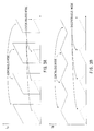
- FIG. 3A is plot of the typical input current waveform for a buck type switching regulator in continuous mode and discontinuous mode.
- FIG. 3B is plot of the typical input current waveform for a boost type switching regulator in continuous mode and discontinuous mode.
- FIG. 4A illustrates a sample set of control waveforms and input power source current for multiple buck switching regulators utilizing sequential switching of switching transistors.
- FIG. 4B illustrates a sample set of control waveforms and input power source current for multiple boost switching regulators utilizing sequential switching of switching transistors.
- FIG. 5 is a block diagram illustrating a control system that sequentially switches the switching transistors of multiple switching regulators.
- FIG. 6. illustrates a sample set of control waveforms for multiple switching regulators utilizing the simultaneous switching of two regulators sequentially after a first regulator.
- FIG. 7 is a block diagram illustrating a control system that switches two switches sequentially after switching a first regulator.
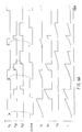
- FIG. 8 illustrates a sample set of control waveforms for multiple switching regulators switching transistors at predetermined times.
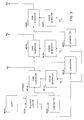
- FIG. 9 is a block diagram illustrating a control system that switches on the switching transistors of multiple switching regulators at predetermined times.
- FIG. 1 is a schematic diagram of multiple buck type switching regulators with the same input power source.
- FIG. 2 is a schematic diagram of multiple boost type switching regulators with the same input power source.
- These types of regulators were chosen for exemplary purposes only. It should be understood that this invention is applicable to other types of switching regulators known to those of ordinary skill in the art.
- the type of switch in these regulators is shown as an N-channel MOSFET. This is also only for exemplary purposes and other types of switching devices know to those skilled in the art could be used.
- the input voltage to the multiple regulators 1010, 1020, and 1030 is V i .
- the aggregate input current into the multiple regulators is I i .
- Input current into the first regulator 1010 is I i1 .
- the input current into the second regulator 1020 is I i2 and so on, such that the input current into the third regulator 1030 is I i3 .
- first regulator 1010 is shown comprising switching transistor S1, 1012, diode 1014, inductor L1, 105, and filter capacitor C1 1016.
- First regulator 1010 is shown as producing output voltage V 1 into load LOAD1 1018.
- Switching transistor S1 is shown as an N-type enhancement MOSFET with its drain connected to V i , its body and source connected to the cathode of diode 1014, and its gate connected to control voltage V g1 .
- the anode of diode 1014 is shown being connected to the reference node of V i , gnd.
- the cathode of diode 1014, source and body of S1 are also connected a first terminal of inductor L1, 1015.
- the second terminal of L1, 1015 is connected to a first terminal of filter capacitor C1, 1016.
- the second terminal of filter capacitor C1, 1016 is shown connected to gnd.
- the load on the first regulator LOAD1, 1018 is shown connected in parallel with filter capacitor C1 1016.
- Second regulator 1020 is shown with the same circuit design as first regulator 1010. Second regulator 1020 is shown comprising switching transistor S2, 1022, diode 1024, inductor L2, 1025, and filter capacitor C2 1026. Second regulator 1020 is shown as producing output voltage V 2 into load LOAD2 1028. Switching transistor S2 is shown as an N-type enhancement MOSFET with its drain connected to V i , its body and source connected to the cathode of diode 1024, and its gate connected to control voltage V g2 . The anode of diode 1024 is shown being connected to the reference node of V i , gnd.
- the cathode of diode 1024, source and body of S2, are also connected a first terminal of inductor L2, 1025.
- the second terminal of L2, 1025 is connected to a first terminal of filter capacitor C2, 1026.
- the second terminal of filter capacitor C2, 1026 is shown connected to gnd.
- the load on the first regulator LOAD2, 1028 is shown connected in parallel with filter capacitor C2 1026.
- Third regulator 1030 is shown with the same circuit design as first regulator 1010 and second regulator 1020.
- Third regulator 1030 is shown comprising switching transistor S3, 1032, diode 1034, inductor L3, 1035, and filter capacitor C3 1036.
- Second regulator 1030 is shown as producing output voltage V 3 into load LOAD3 1038.
- Switching transistor S3 is shown as an N-type enhancement MOSFET with its drain connected to V i , its body and source connected to the cathode of diode 1034, and its gate connected to control voltage V g3 .
- the anode of diode 1034 is shown being connected to the reference node of V i , gnd.
- the cathode of diode 1034, source and body of S3, are also connected a first terminal of inductor L3, 1035.
- the second terminal of L3, 1035 is connected to a first terminal of filter capacitor C3, 1036.
- the second terminal of filter capacitor C3, 1036 is shown connected to gnd.
- the load on the first regulator LOAD3, 1038 is shown connected in parallel with filter capacitor C3 1036.
- regulators 1010, 1020, and 1030 are intended to represent an arbitrary number of supply voltages generated from a single input power source.
- the basic design of these supplies is a buck regulator type design.
- boost type or buck-boost type, or a combination of switching regulator types.
- the input voltage to the multiple regulators 2010, 2020, and 2030 is V i .
- the aggregate input current into the multiple regulators is I i .
- Input current into the first regulator 2010 is I i1 .
- the input current into the second regulator 2020 is I i2 and so on, such that the input current into the third regulator 2030 is I i3 .
- first regulator 2010 is shown comprising switching transistor S1, 2014, diode 2015, inductor L1, 2012, and filter capacitor C1 2016.
- First regulator 2010 is shown as producing output voltage V 1 into load LOAD1 2018.
- Inductor L1 2012 is shown connected between V i and the drain of switching transistor S1 2014.
- Switching transistor S1 is shown as an N-type enhancement MOSFET with its body and source connected to the reference node of V i , gnd, and its gate connected to control voltage V g1 .
- the anode of diode 2015 is connected to the drain of switching transistor S1 2014.
- the cathode of diode 2015 is connected a first terminal of filter capacitor C1 2016.
- the second terminal of C1 2016 is connected to gnd.
- the load on the first regulator LOAD1, 2018 is shown connected in parallel with filter capacitor C1 2016.
- second regulator 2020 is shown comprising switching transistor S2, 2024, diode 2025, inductor L2, 2022, and filter capacitor C2 2026.
- Second regulator 2020 is shown as producing output voltage V 2 into load LOAD2 2028.
- Inductor L2 2022 is shown connected between V i and the drain of switching transistor S2 2024.
- Switching transistor S2 is shown as an N-type enhancement MOSFET with its body and source connected to the reference node of V i , gnd, and its gate connected to control voltage V g2 .
- the anode of diode 2025 is connected to the drain of switching transistor S2 2024.
- the cathode of diode 2025 is connected a first terminal of filter capacitor C2 2026.
- the second terminal of C2 2026 is connected to gnd.
- the load on the first regulator LOAD2, 2028 is shown connected in parallel with filter capacitor C2 2026.
- third regulator 2030 is shown comprising switching transistor S3, 2034, diode 2035, inductor L3, 2032, and filter capacitor C3 2036.
- Second regulator 2030 is shown as producing output voltage V 3 into load LOAD3 2038.
- Inductor L3 2032 is shown connected between V i and the drain of switching transistor S3 2034.
- Switching transistor S3 is shown as an N-type enhancement MOSFET with its body and source connected to the reference node of V i , gnd, and its gate connected to control voltage V g3 .
- the anode of diode 2035 is connected to the drain of switching transistor S3 2034.
- the cathode of diode 2035 is connected a first terminal of filter capacitor C3 2036.
- the second terminal of C3 2036 is connected to gnd.
- the load on the first regulator LOAD3, 2038 is shown connected in parallel with filter capacitor C3 2036.
- FIG. 3A is a plot of the typical input current waveforms for a buck type switching regulator in continuous mode and discontinuous mode.
- FIG. 3B is plot of the typical input current waveforms for a boost type switching regulator in continuous mode and discontinuous mode. Note that these current waveforms come to a peak before declining. When the current peaks of multiple regulators drawing from the same input power source coincide roughly in time a large input current peak occurs. This invention helps prevent that condition so that the overall peak input current is reduced.
- FIG. 4A illustrates an example set of control signals and current waveforms for sequential switching of transistors in multiple buck regulators.
- Signal CLOCK is a periodic waveform that sets triggers the switching of the first regulator in the sequence. That regulator is controlled by V g1 .
- V g1 rises turning on the switching transistor in the first regulator when CLOCK falls.
- V g2 rises turning on the switching transistor in the second regulator in the sequence.
- V g3 rises turning on the switching transistor in the third regulator in the sequence.
- V g3 falls turning off the switching transistor in the third regulator.
- the falling edge of signal CLOCK starts the sequence again.
- FIG. 4A Also shown on FIG. 4A are example input currents (I i1 , I i2 , I i3 ) for each of the three power supplies when controlled by sequenced control signals described above and shown in FIG. 4A.
- the sum of these input currents is the total input current load on the input power source, I i .
- the sequenced switching of the transistors in the three supplies in this example reduces the total current load when compared to the situation where all three switching transistors are switched so that all three supplies reach their peak current at about the same time.
- each switching transistor of each regulator may be set according to an error signal derived from the output voltage of that regulator.
- the system may not operate with optimally low peak input current depending on the dynamic loading, but regulation should be maintained as long as the signal to switch off the transistor in a particular regulator occurs before or nearly the same time as the signal to switch on that particular transistor occurs again.
- arranging the sequence that supplies from the largest input anticipated current load to the smallest will help reduce the peak input current even when there are two or more switching transistors in different supplies on at the same time.
- FIG. 4B illustrates an example set of control signals and current waveforms for sequential switching of transistors in multiple boost regulators.
- Signal CLOCK is a periodic waveform that sets triggers the switching of the first regulator in the sequence. That regulator is controlled by V g1 .
- V g1 rises turning on the switching transistor in the first regulator when CLOCK falls.
- V g2 rises turning on the switching transistor in the second regulator in the sequence.
- V g3 rises turning on the switching transistor in the third regulator in the sequence.
- V g3 falls turning off the switching transistor in the third regulator.
- the falling edge of signal CLOCK starts the sequence again.
- FIG. 4B Also shown on FIG. 4B are example input currents (I i1 , I i2 , I i3 ) for each of the three power supplies when controlled by sequenced control signals described above and shown in FIG. 4B.
- the sum of these input currents is the total input current load on the input power source, I i .
- the sequenced switching of the transistors in the three supplies in this example reduces the total current load when compared to the situation where all three switching transistors are switched so that all three supplies reach their peak current at about the same time.
- each switching transistor of each regulator may be set according to an error signal derived from the output voltage of that regulator.
- the system may not operate with optimally low peak input current depending on the dynamic loading, but regulation should be maintained as long as the signal to switch off the transistor in a particular regulator occurs before or nearly the same time as the signal to switch on that particular transistor occurs again.
- arranging the sequence that supplies from the largest input anticipated current load to the smallest will help reduce the peak input current even when there are two or more switching transistors in different supplies on at the same time.
- FIG. 5 illustrates a block diagram of a system that sequentially switches the transistors in multiple supplies.
- Clock generator 5002 sends a signal (CLOCK) to pulse width modulation (PWM) generator 5004 that turns on the switching transistor of the first regulator in the sequence via signal V g1 .
- the length of time that V g1 remains active keeping the switching transistor of the first regulator in the sequence on depends on a signal from error generator 5010.
- the signal from error generator 5010 depends on the output voltage of the first regulator in the sequence.
- this control system is used with three supplies as shown in FIG. 1, this would be V 1 for regulator 1010.
- PWM generator 5006 turns on the switching transistor of the second regulator in the sequence via signal V g2 .
- the length of time that V g2 remains active keeping the switching transistor of the second regulator in the sequence on depends on a signal from error generator 5012.
- the signal from error generator 5012 depends on the output voltage of the second regulator in the sequence.
- PWM generator 5008 turns on the switching transistor of the third regulator in the sequence via signal V g3 .
- the length of time that V g3 remains active keeping the switching transistor of the third regulator in the sequence on depends on a signal from error generator 5014.
- the signal from error generator 5014 depends on the output voltage of the third regulator in the sequence.
- FIG. 6. illustrates the control waveforms for multiple switching regulators utilizing the simultaneous switching of two regulators sequentially after a first regulator.
- signal CLOCK is a periodic waveform that sets triggers the switching of the first regulator in the sequence. That regulator is controlled by V g1 .
- V g1 rises turning on the switching transistor in the first regulator when CLOCK falls.
- Vg2 and V g3 rise turning on the switching transistors in the second and third power supplies.
- V g2 and V g3 then fall independent of each other switching off the switching transistors in the second and third power supplies.
- the falling edge of signal CLOCK starts the sequence again.
- Simultaneous turning on the switching transistors in two or more regulators allows a faster cycle time for signal CLOCK. This is particularly useful when two of the regulators are known, or expected, to have low input power source current when compared to other supplies. These two regulators may then be switched on at the same time to allow for a faster cycle time for signal CLOCK without greatly affecting the peak total input power source current.
- a fixed delay may be introduced from the switching on of the transistor in one regulator, to the switching on of the transistor in another. This may be useful when the input current to two regulators are thought to roughly track each other, but one is expected to mostly be larger than the other.
- FIG. 7 is a block diagram illustrating a control system that switches two switches sequentially after switching a first regulator.
- Clock generator 7002 sends a signal (CLOCK) to pulse width modulation (PWM) generator 7004 that turns on the switching transistor of the first regulator in the sequence via signal V g1 .
- the length of time that V g1 remains active keeping the switching transistor of the first regulator in the sequence on depends on a signal from error generator 7010.
- the signal from error generator 7010 depends on the output voltage of the first regulator in the sequence.
- this control system is used with three regulators as shown in FIG. 1, this would be V 1 for regulator 1010.
- this control system is used with three regulators as shown in FIG. 2, this would be V 1 for regulator 2010.
- PWM generator 7006 turns on the switching transistor of the second regulator in the sequence via signal V g2 .
- the length of time that V g2 remains active keeping the switching transistor of the second regulator in the sequence on depends on a signal from error generator 7012.
- the signal from error generator 7012 depends on the output voltage of the second regulator in the sequence.
- PWM generator 7008 turns on the switching transistor of the third regulator in the sequence via signal V g3 after an optional time delay 7016. If no time delay is wanted, PWM generator 7008 turns on the switching transistor of the third regulator in the sequence via signal V g3 at the same time that PWM generator 7006 turns on the switching transistor of the second regulator via signal V g2 .
- the length of time that V g3 remains active keeping the switching transistor of the third regulator in the sequence on depends on a signal from error generator 7014.
- the signal from error generator 7014 depends on the output voltage of the third regulator in the sequence. When this control system is used with three regulators as shown in FIG. 1, this would be V 3 for regulator 1030. When this control system is used with three regulators as shown in FIG. 2, this would be V 3 for regulator 2030.
- FIG. 8 illustrates control waveforms for multiple switching regulators that turn on switching transistors at predetermined times.
- Signal CLOCK is a periodic waveform that is used as the timebase for turning on the switching transistors in the multiple supplies.
- Signal FIRST is a signal that when active shows which cycle of CLOCK marks the beginning of a new switching cycle.
- the switching transistor in the first regulator is turned on via V g1 rising during the first cycle of CLOCK.
- the switching transistor in the second regulator is turned on via V g2 rising during the second cycle of CLOCK.
- the switching transistor in the third regulator is turned on via V g3 rising during the forth cycle of CLOCK.
- Each of the control signals V g1 , V g2 , and V g3 fall independently.
- the falling edge of signal CLOCK starts the sequence again.
- the activation of signal FIRST starts a new switching cycle.
- FIG. 9 is a block diagram illustrating a control system that can switch on switching transistors of multiple switching regulators at predetermined times.
- Clock generator 9002 produces signal CLOCK that provides a periodic waveform that is used as the timebase for the system.
- CLOCK is input to rollover counter 9004.
- Rollover counter 9004 takes the input pulses of clock and produces a digital output that is a count of those pulses.
- the rollover counter resets its output to a first count number and activates signal FIRST until another pulse is received on CLOCK.
- comparator 9006 The count output of rollover counter is input to comparators 9006, 9008, and 9010. Each of these comparators produces a signal when its input matches a predetermined number. If FIG. 8 is used as an example, then comparator 9006 would produce a signal when its input was 1, comparator 9008 would produce a signal when its input was 2, and comparator 9010 would produce a signal when its inputs was 4.
- the signal generated by comparator 9006 triggers pulse width modulation (PWM) generator 9006 to turn on the switching transistor of a first regulator via signal V g1
- PWM pulse width modulation
- the length of time that V g1 remains active keeping the switching transistor of that regulator on depends on a signal from error generator 9014.
- the signal from error generator 9014 depends on the output voltage of that regulator. When this control system is used with three supplies as shown in FIG. 1, this output voltage would be V 1 for regulator 1010. When this control system is used with three supplies as shown in FIG. 2, this output voltage would be V 1 for regulator 2010.
- the signal generated by comparator 9008 triggers pulse width modulation (PWM) generator 9016 to turn on the switching transistor of a second regulator via signal V g2 .
- PWM pulse width modulation
- the length of time that V g2 remains active keeping the switching transistor of that regulator on depends on a signal from error generator 9018.
- the signal from error generator 9018 depends on the output voltage of that regulator. When this control system is used with three regulators as shown in FIG. 1, this output voltage would be V 2 for regulator 1020. When this control system is used with three regulators as shown in FIG. 2, this output voltage would be V 2 for regulator 2020.
- the signal generated by comparator 9010 triggers pulse width modulation (PWM) generator 9020 to turn on the switching transistor of a third regulator via signal V g3 .
- PWM pulse width modulation
- the length of time that V g3 remains active keeping the switching transistor of that regulator on depends on a signal from error generator 9022.
- the signal from error generator 9022 depends on the output voltage of that regulator. When this control system is used with three regulators as shown in FIG. 1, this output voltage would be V 2 for regulator 1020. When this control system is used with three regulators as shown in FIG. 2, this output voltage would be V 2 for regulator 2020.
- One way to choose the predetermined times to switch on the switching transistors of the multiple supplies is to choose the times that will result in the minimum peak input power source current. If the maximum input currents to each regulator for each load situation are known or estimated, the length of each control (V g1 , V g2 , etc.) pulse can be determined. This information, the input voltage, and the design of each regulator give enough data to determine the input current waveform for each regulator in a given load situation. These input current waveforms can then be used to determine when to start each control pulse so that the peak input power source current is minimized.
- the CLOCK signal is shown as having a constant period.
- a variable period clock may be used in any of these.
- This variable period (or frequency) clock may be derived in response to changing loads on the multiple power supplies, or some other control system variables.
- these systems have been shown as block diagrams of discrete blocks, it should be understood that any of these systems could be implemented using a microcontroller, other processor, or custom integrated circuit. Any of these systems may also take into account more variables than is shown when arranging, or timing, control pulses. For example, a microcontroller may know that it is about to perform a number of functions that require a great deal of power on a certain voltage supply. Before performing those operations, the microcontroller may rearrange, or change the timing of, the control pulses so that when these functions are performed, the peak input power source current will be minimized when that regulator begins to pull greater input current.
Landscapes
- Engineering & Computer Science (AREA)
- Power Engineering (AREA)
- Dc-Dc Converters (AREA)
- Continuous-Control Power Sources That Use Transistors (AREA)
Abstract
Description
Claims (10)
- A power supply, comprising:an input power source;a first switching regulator (1010, 2010), said first switching regulator increasing and decreasing current drawn by said first switching regulator from said input power source;a second switching regulator (1020, 2020), said second switching regulator increasing and decreasing current drawn by said second switching regulator from said input power source; and,a switching controller, said switching controller causing said second switching regulator to increase current drawn by said second switching regulator from said input power source after said switching controller causes said first switching regulator to decrease current drawn by said first switching regulator from said input power source.
- The power supply of claim 1, further comprising:
a third switching regulator (1030, 2030), said third switching regulator increasing and decreasing current drawn by said third switching regulator from said input power source and wherein said switching controller causes said third switching regulator to increase current drawn by said third switching regulator from said input power source after said switching controller causes said second switching regulator to decrease current drawn by said second switching regulator from said input power source. - The power supply of claim 1, further comprising:
a third switching regulator (1030, 2030), said third switching regulator increasing and decreasing current drawn by said third switching regulator from said input power source and wherein said switching controller causes said third switching regulator to increase current drawn by said third switching regulator from said input power source after said switching controller causes said first switching regulator to decrease current drawn by said first switching regulator from said input power source. - The power supply of claim 3, wherein said switching controller causes said third switching regulator to increase current drawn by said third switching regulator from said input power source a fixed time delay after said switching controller causes said first switching regulator to decrease current drawn by said first switching regulator from said input power source.
- The power supply of claim 1, further comprising:
a third switching regulator (1030, 2030), said third switching regulator increasing and decreasing current drawn by said third switching regulator from said input power source and wherein said switching controller causes the order of the increasing and decreasing of current drawn by said second switching regulator and the increasing and decreasing of current drawn by said third regulator to lower the peak amount of current drawn from said input power source. - The power supply of claim 5 wherein said controller also alters the timing of the increasing and decreasing of the current drawn by said second switching regulator and the timing of the increasing and the decreasing of the current drawn by the third switching regulator to lower the peak amount of current drawn from said input power source.
- A power supply, comprising:an input power source;a first switching regulator (1010, 2010), said first switching regulator drawing current from said input power source;a second switching regulator (1010, 2010), said second switching regulator drawing current from said input power source; and,a switching controller, said switching controller causing said first switching regulator to change the current drawn by said first switching regulator from said input power source at a first time in a cycle and said switching controller causing said second switching regulator to change the current drawn by said second switching regulator from said input power source at a second time in said cycle.
- The power supply of claim 7 wherein said first time and said second time are chosen to lower a peak input current drawn from said input power source.
- The power supply of claim 8 wherein said switching controller chooses said first time and said second time.
- A power supply, comprising:an input power source;a plurality of switching regulators (1010, 1020, 1030) drawing input currents from said input power source; and,a switching controller, said switching controller causing said input currents to initiate a change in magnitude of said input currents in a first direction in a first sequence.
Applications Claiming Priority (2)
| Application Number | Priority Date | Filing Date | Title |
|---|---|---|---|
| US09/437,669 US6265855B1 (en) | 1999-11-10 | 1999-11-10 | Coordinated switching in a multiple switching regulator system to lower peak current load |
| US437669 | 1999-11-10 |
Publications (3)
| Publication Number | Publication Date |
|---|---|
| EP1104949A2 true EP1104949A2 (en) | 2001-06-06 |
| EP1104949A3 EP1104949A3 (en) | 2002-01-02 |
| EP1104949B1 EP1104949B1 (en) | 2003-07-09 |
Family
ID=23737398
Family Applications (1)
| Application Number | Title | Priority Date | Filing Date |
|---|---|---|---|
| EP00309850A Expired - Lifetime EP1104949B1 (en) | 1999-11-10 | 2000-11-06 | Coordinated switching in a multiple switching regulator system to lower peak current load |
Country Status (5)
| Country | Link |
|---|---|
| US (2) | US6265855B1 (en) |
| EP (1) | EP1104949B1 (en) |
| JP (1) | JP3628955B2 (en) |
| CN (2) | CN1171373C (en) |
| DE (1) | DE60003771T2 (en) |
Families Citing this family (28)
| Publication number | Priority date | Publication date | Assignee | Title |
|---|---|---|---|---|
| US6816978B1 (en) * | 2000-06-07 | 2004-11-09 | Hewlett-Packard Development Company, L.P. | System and method for adjusting an input voltage to a switching power supply while keeping the output voltage constant |
| US6747855B2 (en) * | 2002-01-24 | 2004-06-08 | Intel Corporation | Innovative regulation characteristics in multiple supply voltages |
| JP3688257B2 (en) * | 2002-09-27 | 2005-08-24 | 株式会社リコー | Power supply device and mobile phone |
| US6819011B2 (en) * | 2002-11-14 | 2004-11-16 | Fyre Storm, Inc. | Switching power converter controller with watchdog timer |
| WO2004066050A1 (en) * | 2003-01-17 | 2004-08-05 | Freescale Semiconductor, Inc. | Power management system |
| JP3851303B2 (en) * | 2003-09-08 | 2006-11-29 | ローム株式会社 | Multi-output type power supply device and portable device using the same |
| TW200516821A (en) * | 2003-11-14 | 2005-05-16 | Hon Hai Prec Ind Co Ltd | System and method for starting up devices orderly |
| CN1627412A (en) * | 2003-12-13 | 2005-06-15 | 鸿富锦精密工业(深圳)有限公司 | Control circuit and method for starting up multiple hard disks with multiple backboards in sequence |
| JP4238872B2 (en) * | 2004-02-03 | 2009-03-18 | 株式会社村田製作所 | Switching power supply |
| US7400064B2 (en) * | 2005-04-22 | 2008-07-15 | Texas Instruments Incorporated | DC/DC power converter |
| US7276885B1 (en) * | 2005-05-09 | 2007-10-02 | National Semiconductor Corporation | Apparatus and method for power sequencing for a power management unit |
| US7723864B2 (en) * | 2005-07-26 | 2010-05-25 | Norgren, Inc. | AC-to-DC electrical switching circuit |
| US20070090815A1 (en) * | 2005-10-24 | 2007-04-26 | Faraday Technology Corp. | Integrated circuit with power gating function |
| CN101313632B (en) * | 2005-12-12 | 2012-04-25 | 三菱电机株式会社 | Light emitting diode lighting device and vehicle light lighting device using same |
| JP2007174856A (en) * | 2005-12-26 | 2007-07-05 | Matsushita Electric Ind Co Ltd | Booster and step-down device |
| US8064179B2 (en) * | 2006-09-05 | 2011-11-22 | Silicon Laboratories Inc. | Integrated circuit including a switching regulator design for power over Ethernet devices |
| US7629779B2 (en) * | 2006-09-21 | 2009-12-08 | Intel Corporation | Multiple output multiple topology voltage converter |
| US20080157597A1 (en) * | 2006-12-27 | 2008-07-03 | Annabelle Pratt | Multiple output isolated converter circuit |
| US7911190B2 (en) * | 2007-02-14 | 2011-03-22 | Texas Instruments Incorporated | Regulator with automatic power output device detection |
| US20090015066A1 (en) * | 2007-07-10 | 2009-01-15 | Yazaki North America, Inc. | Close-loop relay driver with equal-phase interval |
| JP5239360B2 (en) * | 2008-01-31 | 2013-07-17 | 株式会社リコー | Switching power supply circuit |
| US8164378B2 (en) * | 2008-05-06 | 2012-04-24 | Freescale Semiconductor, Inc. | Device and technique for transistor well biasing |
| TWI381622B (en) * | 2009-10-05 | 2013-01-01 | Anpec Electronics Corp | Power supply with synchronized clocks and related dc-dc converter |
| US8330441B1 (en) * | 2010-01-25 | 2012-12-11 | National Semiconductor Corporation | Technique for reducing crosstalk interference between integrated switching regulators |
| US9041452B2 (en) * | 2010-01-27 | 2015-05-26 | Silicon Laboratories Inc. | Circuit and method of clocking multiple digital circuits in multiple phases |
| KR20160001093A (en) * | 2014-06-26 | 2016-01-06 | 삼성전자주식회사 | Method for controlling switching regulator and electronic device |
| JP2017153218A (en) * | 2016-02-23 | 2017-08-31 | 富士通株式会社 | Power supply device |
| CN116088625B (en) * | 2023-04-07 | 2023-06-13 | 河北极太科技有限公司 | Output voltage regulating circuit |
Family Cites Families (11)
| Publication number | Priority date | Publication date | Assignee | Title |
|---|---|---|---|---|
| US4034232A (en) * | 1976-06-01 | 1977-07-05 | Burroughs Corporation | System for synchronizing and phase shifting switching regulators |
| JPS5872370A (en) * | 1981-10-23 | 1983-04-30 | Hitachi Ltd | Switching regulator |
| US5045712A (en) * | 1985-03-28 | 1991-09-03 | Raytheon Company | Synchronized switched mode power supplies |
| JPH0595672A (en) * | 1991-10-01 | 1993-04-16 | Fujitsu Ltd | Starting circuit for multiple output power supply |
| JP2571942Y2 (en) * | 1992-10-12 | 1998-05-20 | ネミック・ラムダ株式会社 | Boost converter |
| US5442534A (en) * | 1993-02-23 | 1995-08-15 | California Institute Of Technology | Isolated multiple output Cuk converter with primary input voltage regulation feedback loop decoupled from secondary load regulation loops |
| JP3359097B2 (en) * | 1993-06-11 | 2002-12-24 | オリジン電気株式会社 | Multi-output power supply |
| JPH09289773A (en) * | 1996-04-22 | 1997-11-04 | Mitsubishi Electric Corp | Multi-output switching power supply |
| US5905369A (en) * | 1996-10-17 | 1999-05-18 | Matsushita Electric Industrial Co., Ltd. | Variable frequency switching of synchronized interleaved switching converters |
| JP3148171B2 (en) * | 1998-01-12 | 2001-03-19 | 株式会社日本プロテクター | Switching regulator |
| US6043634A (en) * | 1998-12-22 | 2000-03-28 | Intel Corporation | Interleaved switching regulator |
-
1999
- 1999-11-10 US US09/437,669 patent/US6265855B1/en not_active Expired - Fee Related
-
2000
- 2000-08-10 CN CNB001226487A patent/CN1171373C/en not_active Expired - Fee Related
- 2000-08-10 CN CNA2004100074035A patent/CN1551474A/en active Pending
- 2000-11-06 EP EP00309850A patent/EP1104949B1/en not_active Expired - Lifetime
- 2000-11-06 JP JP2000337743A patent/JP3628955B2/en not_active Expired - Fee Related
- 2000-11-06 DE DE60003771T patent/DE60003771T2/en not_active Expired - Fee Related
-
2001
- 2001-04-25 US US09/842,334 patent/US6437548B2/en not_active Expired - Lifetime
Also Published As
| Publication number | Publication date |
|---|---|
| JP3628955B2 (en) | 2005-03-16 |
| CN1551474A (en) | 2004-12-01 |
| DE60003771D1 (en) | 2003-08-14 |
| CN1296202A (en) | 2001-05-23 |
| EP1104949B1 (en) | 2003-07-09 |
| EP1104949A3 (en) | 2002-01-02 |
| JP2001161061A (en) | 2001-06-12 |
| US6437548B2 (en) | 2002-08-20 |
| CN1171373C (en) | 2004-10-13 |
| US20010015639A1 (en) | 2001-08-23 |
| DE60003771T2 (en) | 2004-06-17 |
| US6265855B1 (en) | 2001-07-24 |
Similar Documents
| Publication | Publication Date | Title |
|---|---|---|
| EP1104949B1 (en) | Coordinated switching in a multiple switching regulator system to lower peak current load | |
| US5617015A (en) | Multiple output regulator with time sequencing | |
| US6037755A (en) | Switching controller for a buck+boost converter and method of operation thereof | |
| US6900620B2 (en) | Switching regulator having two or more outputs | |
| US7075277B2 (en) | DC-DC converter | |
| KR101243595B1 (en) | Multi output power supply | |
| US6903536B2 (en) | PFC-PWM controller having interleaved switching | |
| US7498786B2 (en) | Digital control of switching voltage regulators | |
| US6861826B2 (en) | Timing circuit for synchronous DC/DC control to reduce synchronous rectifier body diode conduction | |
| US20110101946A1 (en) | Voltage converters | |
| US20050088160A1 (en) | Multi output DC-DC converter | |
| JP2006050894A (en) | Power feeding for multiple load by dc-dc converter | |
| JP2002209376A (en) | Control device and control method for voltage regulator | |
| US20010043059A1 (en) | Integrated low ripple, high frequency hysteretic controller for DC-DC converters | |
| CN112311236A (en) | Switched mode power supply | |
| JP2006014559A (en) | Dc/dc converter | |
| US20260100650A1 (en) | Transient control scheme for multiphase power converters | |
| CN100359599C (en) | Power-supply device and its power supply method | |
| US20020079948A1 (en) | Bootstrap circuit in DC/DC static converters | |
| CN118232655A (en) | Minimum inductance peak current circuit for low-power-consumption switching power supply | |
| JP7452395B2 (en) | Switching power supply control device | |
| EP1198057A2 (en) | A power supply | |
| US20250247004A1 (en) | Switching power supply device | |
| CN219875494U (en) | voltage conversion system | |
| US20250183800A1 (en) | Dc-dc converter |
Legal Events
| Date | Code | Title | Description |
|---|---|---|---|
| PUAI | Public reference made under article 153(3) epc to a published international application that has entered the european phase |
Free format text: ORIGINAL CODE: 0009012 |
|
| AK | Designated contracting states |
Kind code of ref document: A2 Designated state(s): DE FR GB Kind code of ref document: A2 Designated state(s): AT BE CH CY DE DK ES FI FR GB GR IE IT LI LU MC NL PT SE TR |
|
| AX | Request for extension of the european patent |
Free format text: AL;LT;LV;MK;RO;SI |
|
| PUAL | Search report despatched |
Free format text: ORIGINAL CODE: 0009013 |
|
| AK | Designated contracting states |
Kind code of ref document: A3 Designated state(s): AT BE CH CY DE DK ES FI FR GB GR IE IT LI LU MC NL PT SE TR |
|
| AX | Request for extension of the european patent |
Free format text: AL;LT;LV;MK;RO;SI |
|
| 17P | Request for examination filed |
Effective date: 20020521 |
|
| AKX | Designation fees paid |
Free format text: DE FR GB |
|
| 17Q | First examination report despatched |
Effective date: 20020814 |
|
| GRAH | Despatch of communication of intention to grant a patent |
Free format text: ORIGINAL CODE: EPIDOS IGRA |
|
| GRAH | Despatch of communication of intention to grant a patent |
Free format text: ORIGINAL CODE: EPIDOS IGRA |
|
| GRAA | (expected) grant |
Free format text: ORIGINAL CODE: 0009210 |
|
| AK | Designated contracting states |
Designated state(s): DE FR GB |
|
| REG | Reference to a national code |
Ref country code: GB Ref legal event code: FG4D |
|
| REF | Corresponds to: |
Ref document number: 60003771 Country of ref document: DE Date of ref document: 20030814 Kind code of ref document: P |
|
| REG | Reference to a national code |
Ref country code: IE Ref legal event code: FG4D |
|
| PLBE | No opposition filed within time limit |
Free format text: ORIGINAL CODE: 0009261 |
|
| STAA | Information on the status of an ep patent application or granted ep patent |
Free format text: STATUS: NO OPPOSITION FILED WITHIN TIME LIMIT |
|
| 26N | No opposition filed |
Effective date: 20040414 |
|
| REG | Reference to a national code |
Ref country code: IE Ref legal event code: MM4A |
|
| PGFP | Annual fee paid to national office [announced via postgrant information from national office to epo] |
Ref country code: FR Payment date: 20070207 Year of fee payment: 7 Ref country code: GB Payment date: 20071128 Year of fee payment: 8 |
|
| PGFP | Annual fee paid to national office [announced via postgrant information from national office to epo] |
Ref country code: DE Payment date: 20071221 Year of fee payment: 8 |
|
| REG | Reference to a national code |
Ref country code: FR Ref legal event code: ST Effective date: 20080930 |
|
| PG25 | Lapsed in a contracting state [announced via postgrant information from national office to epo] |
Ref country code: FR Free format text: LAPSE BECAUSE OF NON-PAYMENT OF DUE FEES Effective date: 20071130 |
|
| GBPC | Gb: european patent ceased through non-payment of renewal fee |
Effective date: 20081106 |
|
| PG25 | Lapsed in a contracting state [announced via postgrant information from national office to epo] |
Ref country code: DE Free format text: LAPSE BECAUSE OF NON-PAYMENT OF DUE FEES Effective date: 20090603 |
|
| PG25 | Lapsed in a contracting state [announced via postgrant information from national office to epo] |
Ref country code: GB Free format text: LAPSE BECAUSE OF NON-PAYMENT OF DUE FEES Effective date: 20081106 |