EP1104054A1 - Semiconductor laser - Google Patents
Semiconductor laser Download PDFInfo
- Publication number
- EP1104054A1 EP1104054A1 EP00922939A EP00922939A EP1104054A1 EP 1104054 A1 EP1104054 A1 EP 1104054A1 EP 00922939 A EP00922939 A EP 00922939A EP 00922939 A EP00922939 A EP 00922939A EP 1104054 A1 EP1104054 A1 EP 1104054A1
- Authority
- EP
- European Patent Office
- Prior art keywords
- cavity length
- current
- semiconductor laser
- optical output
- oscillation
- Prior art date
- Legal status (The legal status is an assumption and is not a legal conclusion. Google has not performed a legal analysis and makes no representation as to the accuracy of the status listed.)
- Granted
Links
Images


Classifications
-
- H—ELECTRICITY
- H01—ELECTRIC ELEMENTS
- H01S—DEVICES USING THE PROCESS OF LIGHT AMPLIFICATION BY STIMULATED EMISSION OF RADIATION [LASER] TO AMPLIFY OR GENERATE LIGHT; DEVICES USING STIMULATED EMISSION OF ELECTROMAGNETIC RADIATION IN WAVE RANGES OTHER THAN OPTICAL
- H01S5/00—Semiconductor lasers
- H01S5/10—Construction or shape of the optical resonator, e.g. extended or external cavity, coupled cavities, bent-guide, varying width, thickness or composition of the active region
-
- H—ELECTRICITY
- H01—ELECTRIC ELEMENTS
- H01S—DEVICES USING THE PROCESS OF LIGHT AMPLIFICATION BY STIMULATED EMISSION OF RADIATION [LASER] TO AMPLIFY OR GENERATE LIGHT; DEVICES USING STIMULATED EMISSION OF ELECTROMAGNETIC RADIATION IN WAVE RANGES OTHER THAN OPTICAL
- H01S2301/00—Functional characteristics
- H01S2301/16—Semiconductor lasers with special structural design to influence the modes, e.g. specific multimode
-
- H—ELECTRICITY
- H01—ELECTRIC ELEMENTS
- H01S—DEVICES USING THE PROCESS OF LIGHT AMPLIFICATION BY STIMULATED EMISSION OF RADIATION [LASER] TO AMPLIFY OR GENERATE LIGHT; DEVICES USING STIMULATED EMISSION OF ELECTROMAGNETIC RADIATION IN WAVE RANGES OTHER THAN OPTICAL
- H01S5/00—Semiconductor lasers
- H01S5/02—Structural details or components not essential to laser action
- H01S5/028—Coatings ; Treatment of the laser facets, e.g. etching, passivation layers or reflecting layers
- H01S5/0287—Facet reflectivity
-
- H—ELECTRICITY
- H01—ELECTRIC ELEMENTS
- H01S—DEVICES USING THE PROCESS OF LIGHT AMPLIFICATION BY STIMULATED EMISSION OF RADIATION [LASER] TO AMPLIFY OR GENERATE LIGHT; DEVICES USING STIMULATED EMISSION OF ELECTROMAGNETIC RADIATION IN WAVE RANGES OTHER THAN OPTICAL
- H01S5/00—Semiconductor lasers
- H01S5/10—Construction or shape of the optical resonator, e.g. extended or external cavity, coupled cavities, bent-guide, varying width, thickness or composition of the active region
- H01S5/1039—Details on the cavity length
-
- H—ELECTRICITY
- H01—ELECTRIC ELEMENTS
- H01S—DEVICES USING THE PROCESS OF LIGHT AMPLIFICATION BY STIMULATED EMISSION OF RADIATION [LASER] TO AMPLIFY OR GENERATE LIGHT; DEVICES USING STIMULATED EMISSION OF ELECTROMAGNETIC RADIATION IN WAVE RANGES OTHER THAN OPTICAL
- H01S5/00—Semiconductor lasers
- H01S5/20—Structure or shape of the semiconductor body to guide the optical wave ; Confining structures perpendicular to the optical axis, e.g. index or gain guiding, stripe geometry, broad area lasers, gain tailoring, transverse or lateral reflectors, special cladding structures, MQW barrier reflection layers
- H01S5/2004—Confining in the direction perpendicular to the layer structure
-
- H—ELECTRICITY
- H01—ELECTRIC ELEMENTS
- H01S—DEVICES USING THE PROCESS OF LIGHT AMPLIFICATION BY STIMULATED EMISSION OF RADIATION [LASER] TO AMPLIFY OR GENERATE LIGHT; DEVICES USING STIMULATED EMISSION OF ELECTROMAGNETIC RADIATION IN WAVE RANGES OTHER THAN OPTICAL
- H01S5/00—Semiconductor lasers
- H01S5/30—Structure or shape of the active region; Materials used for the active region
- H01S5/32—Structure or shape of the active region; Materials used for the active region comprising PN junctions, e.g. hetero- or double- heterostructures
- H01S5/323—Structure or shape of the active region; Materials used for the active region comprising PN junctions, e.g. hetero- or double- heterostructures in AIIIBV compounds, e.g. AlGaAs-laser, InP-based laser
-
- H—ELECTRICITY
- H01—ELECTRIC ELEMENTS
- H01S—DEVICES USING THE PROCESS OF LIGHT AMPLIFICATION BY STIMULATED EMISSION OF RADIATION [LASER] TO AMPLIFY OR GENERATE LIGHT; DEVICES USING STIMULATED EMISSION OF ELECTROMAGNETIC RADIATION IN WAVE RANGES OTHER THAN OPTICAL
- H01S5/00—Semiconductor lasers
- H01S5/30—Structure or shape of the active region; Materials used for the active region
- H01S5/32—Structure or shape of the active region; Materials used for the active region comprising PN junctions, e.g. hetero- or double- heterostructures
- H01S5/323—Structure or shape of the active region; Materials used for the active region comprising PN junctions, e.g. hetero- or double- heterostructures in AIIIBV compounds, e.g. AlGaAs-laser, InP-based laser
- H01S5/3235—Structure or shape of the active region; Materials used for the active region comprising PN junctions, e.g. hetero- or double- heterostructures in AIIIBV compounds, e.g. AlGaAs-laser, InP-based laser emitting light at a wavelength longer than 1000 nm, e.g. InP-based 1300 nm and 1500 nm lasers
-
- H—ELECTRICITY
- H01—ELECTRIC ELEMENTS
- H01S—DEVICES USING THE PROCESS OF LIGHT AMPLIFICATION BY STIMULATED EMISSION OF RADIATION [LASER] TO AMPLIFY OR GENERATE LIGHT; DEVICES USING STIMULATED EMISSION OF ELECTROMAGNETIC RADIATION IN WAVE RANGES OTHER THAN OPTICAL
- H01S5/00—Semiconductor lasers
- H01S5/30—Structure or shape of the active region; Materials used for the active region
- H01S5/34—Structure or shape of the active region; Materials used for the active region comprising quantum well or superlattice structures, e.g. single quantum well [SQW] lasers, multiple quantum well [MQW] lasers or graded index separate confinement heterostructure [GRINSCH] lasers
- H01S5/3428—Structure or shape of the active region; Materials used for the active region comprising quantum well or superlattice structures, e.g. single quantum well [SQW] lasers, multiple quantum well [MQW] lasers or graded index separate confinement heterostructure [GRINSCH] lasers layer orientation perpendicular to the substrate
Definitions
- the present invention relates to a semiconductor laser device, and more specifically, to a semiconductor laser device adapted for use as a pumping light source for optical fiber amplifier, such as a laser device of the gain-waveguide type that oscillates with a wavelength of, e.g., 0.98 ⁇ m and requires high optical output of hundreds of mW, and capable of ensuring a linear current-optical output characteristic even during high-current operation.
- a semiconductor laser device adapted for use as a pumping light source for optical fiber amplifier, such as a laser device of the gain-waveguide type that oscillates with a wavelength of, e.g., 0.98 ⁇ m and requires high optical output of hundreds of mW, and capable of ensuring a linear current-optical output characteristic even during high-current operation.
- injected carriers are quantized toward quantum wells, and the state density of carrier energy is stepped. Accordingly, the gain coefficient rapidly rises in response to driving current, so that a laser beam can be oscillated even with a low current density.
- the semiconductor laser device of this type delivers higher optical output than a semiconductor laser device that includes an active layer of a bulk semiconductor, so that it is being studied for practical use as a pumping light source for optical fiber amplifier.
- the following semiconductor laser device that oscillates with a wavelength of 0.98 ⁇ m is an object of investigation as a pumping light source for optical fiber amplifier. This device will now be described with reference to the accompanying drawings.
- the device has a layer structure of a semiconductor material, including a lower clad layer 2 of n-AlGaAs, an active layer 3 of a quantum-well structure made of InGaAs and GaAs, an upper clad layer 4 of p-AlGaAs, and a cap layer 5 of p-GaAs, which are stacked in layers on an n-GaAs substrate 1.
- a part of the upper clad layer 4 and the cap layer 5 form a mesa structure, and a passivation film 6 of SiN is formed on the lateral of the mesa structure.
- an upper electrode 7 of Ti/Pt/Au is formed on the cap layer 5 and the passivation film 6, and a lower electrode 8 of AuGe/Ni/Au is formed on the back surface of the substrate 1.
- the device A is manufactured in the following manner.
- the aforesaid layer structure is formed on the n-GaAs substrate by, for example, the MOCVD method, and the upper and lower electrodes are formed on the upper and lower surfaces, respectively, of the layer structure.
- the resulting structure is cleft with a given cavity length L, a low-reflection film 9 of, e.g., SIN is formed on one end face (front facet) S 1 of the structure, and a high-reflection film 10 of, e.g., SiO 2 /Si is formed on the other end face (rear facet) S 2 .
- the cavity length L of the device A with this construction is designed so that the cavity length L is not longer than 1,000 ⁇ m.
- the inventors hereof examined the current-optical output characteristic for the case where the cavity length L of the device A with the layer structure shown in FIGS. 1 and 2 was adjusted to 800 ⁇ m. Thereupon, the characteristic curve of FIG. 3 and the following new knowledge were obtained.
- the inventors hereof first closely examined the oscillation spectrum of the device A. The following is a description of the results of the examination.
- ⁇ the confinement coefficient of the active layer
- K is a factor reflective of the complexity of the electric field for a transverse mode
- n is an equivalent refractive index
- V is the volume of the active layer
- ⁇ is the half width of the spontaneous emission spectrum. It is believed that the smaller the value ⁇ sp, the higher the probability of generation of single longitudinal mode oscillation is.
- the oscillation wavelength ( ⁇ ) is as short as 0.98 ⁇ m, so that ⁇ sp is lowered in proportion to the fourth power of ⁇ . Accordingly, the device A can be supposed to be able to cause single longitudinal mode oscillation with high probability.
- a module is constructed in a manner such that the device A that undergoes single longitudinal mode oscillation is connected to an optical fiber.
- a laser beam generated by single longitudinal mode oscillation has its noise properties lowered under the influence of return light from an end portion of the optical fiber. Further, the oscillation of the laser beam is made unstable by the return light. Accordingly, an optical output fetched from the module and monitor current are rendered unstable.
- the result (2) implies the following situation.
- the longitudinal mode hopping occur which causes substantial discontinuous fluctuations of the optical output when the gain band shifts to the longer wavelength side in response to temperature rise.
- the current-optical output characteristic loses its linearity, so that the first kink (a 1 ) is generated.
- curve C 1 represents a transverse oscillation mode for the case where the injected current is lower than A 2
- curve C 2 represents a transverse oscillation mode for the case where the injected current is near A 2 (or where the second kink a 2 is generated).
- unit-modal transverse oscillation modes shift horizontally from the center position of the device A (or undergo beam steering).
- the direction of emission of the laser beam changes.
- the optical output fetched through the optical fiber fluctuates when the injected current reaches a value approximate to A 2 . This is supposed to result in the generation of the second kink (a 2 ) in the current-optical output characteristic curve.
- An object of the present invention is to provide a semiconductor laser device of the gain-waveguide type, capable of oscillating in a longitudinal multi-mode without generating any kinks in a current-optical output characteristic curve even with use of an injected current of 500 mA or more.
- Another object of the invention is to provide a novel semiconductor laser device adapted for use as a high-reliability pumping light source for optical fiber amplifier and connected to an optical fiber to form a module, in which a bad influence of return light can be restrained and there is no possibility of beam steering in a far field pattern, so that fluctuations of fetched optical output can be inhibited.
- the inventors hereof conducted the following examinations in the process of investigation to achieve the above objects. These examinations will be described first.
- a semiconductor laser device comprising: a laminated structure of a semiconductor material including an active layer formed of a quantum well structure; a low-reflection film formed on one end face of the structure; and a high-reflection film formed on the other end face of the structure; and the cavity length of the device being 1,200 ⁇ m or more.
- the device has a transverse light confinement structure with the transverse refractive index difference of about 1 x 10 -2 for oscillation modes, the reflectance of the low-reflection film on the one end face is 5% or less, and the active layer is formed of one or two quantum well structures.
- FIGS. 1 and 2 A device according to the present invention will now be described with reference to a device A shown by FIGS. 1 and 2.
- the device of the invention has a layer structure such that a semiconductor material is put on a semiconductor substrate by, for example, the MOCVD method, and an active layer 3 is formed of a quantum well structure.
- InP- and GaInNAs-based semiconductor materials may be used in place of the aforesaid materials for the device A.
- the most distinguishing feature of the device of the invention lies in the cavity length (L) of 1,200 ⁇ m or more.
- the intervals between the longitudinal modes which oscillate in the gain band of the oscillation spectrum are shortened in proportion to the reciprocal of the cavity length, as mentioned before. If the cavity length (L) is 1,200 ⁇ m or more and if the quantum well structure is formed of InGaAs/GaAs, the interval between each two adjacent longitudinal oscillation modes is about 0.12 nm spacing.
- This oscillation spectrum shows a longitudinal multi-oscillation mode in which a large number of longitudinal oscillation modes aggregate densely at short intervals in the gain band.
- return light from the optical fiber is also based on the longitudinal multi-mode, so that oscillation of a laser beam can be restrained from being made unstable by the return light.
- the volume of the active layer that is formed of the quantum well structure should preferably be reduced. More specifically, it is advisable to use one or two quantum well structures to form the active layer.
- the value ⁇ sp in expression (1) becomes greater, so that single longitudinal mode oscillation is restrained. If the active layer volume is lessened, moreover, the internal loss of the cavity is reduced, so that the optical output can be improved.
- the cavity length (L) is 1,200 ⁇ m or more, furthermore, the resistance of the device is lowered. If the injected current is increased, therefore, the temperature of the active layer is restrained from rising, so that the laser beam no longer can be moved. In consequence, dislocation of transverse oscillation modes (beam steering), which occurs with conventional devices, never takes place, so that the second kink (a 2 ) cannot be generated in the current-optical output characteristic.
- the cavity length (L) is adjusted to 1,200 ⁇ m (or more), so that the kinks a 1 and a 2 cannot be generated in the current-optical output characteristic curve, and therefore, the linearity of the curve can be maintained.
- a low-reflection film should preferably be formed on one end face (front facet) of the cavity in the device of the invention.
- a low-reflection film with a reflectance of 5% or less is formed on the one end face of the cavity, and a high-reflection film with a reflectance of 80% or more on the other end face.
- a lower clad layer 2 of n-AlGaAs with a thickness of 2 ⁇ m, an active layer 3 formed of two quantum well structures of InGaAs and GaAs, an upper clad layer 4 of p-AlGaAs with a thickness of 2 ⁇ m, and a cap layer 5 of p-GaAs with a thickness of 0.3 ⁇ m were successively stacked in layers on the (100) surface of an n-GaAs substrate 1 by the MOCVD method. Thereafter, the upper part of the resulting layer structure was formed into a mesa structure 4 ⁇ m wide and 2 ⁇ m high, and its whole surface was coated with a passivation film 6 of SiN.
- the back surface of the substrate 1 was polished so that the overall thickness of the substrate was about 100 ⁇ m. After that portion of the passivation film 6 which was situated on the upper surface of the cap layer 5 was removed, an upper electrode 7 of Ti/Pt/Au was formed on the surface of the resulting structure, and a lower electrode 8 of AUGe/Ni/Au was formed on the back surface of the substrate 1.
- a low-reflection film 9 of SiN was formed on one end face S 1 of the bar, and a high-reflection film 10 of SiO 2 /Si was formed on the other end face S 2 .
- the bar was worked into chips, whereupon devices, such as the one shown in FIG. 1, were obtained.
- kink currents injected currents with which kinks are generated were measured.
- the "kink” is defined herein as a state in which the external differential quantum efficiency of an oscillated laser beam is 15% or more of that produced by low injection current, in consideration of the practicality of the device for use as a pumping light source.
- FIG. 6 shows the results of measurement on the kink (a 1 ) that is attributable to jumping of longitudinal modes.
- the kink (a 1 ) current value of a device having the cavity length (L) of 800 ⁇ m is 200 mA, and that of a device having the cavity length (L) of 1,200 ⁇ m is 350 mA.
- currents not higher than 700 mA do not cause generation of the kink (a 1 ).
- FIG. 7 shows the results of measurement on the kink (a 2 ) that is attributable to beam steering for the time of high current injection.
- the kink (a 2 ) current value of the device having the cavity length (L) of 800 ⁇ m is 400 mA
- that of the device having the cavity length (L) of 1,200 ⁇ m is 550 mA
- that of the device having the cavity length (L) of 1,500 ⁇ m is 700 mA.
- the greater the cavity length (L) the higher the current value that causes beam steering is.
- operating voltages for the devices with the cavity lengths of 800 ⁇ m, 1,200 ⁇ m, and 1,500 ⁇ m are 2.1 V, 1.9 V, and 1.75 V, respectively.
- L the greater the cavity length (L), the lower the operating voltage is.
- FIG. 8 shows an oscillation spectrum of the device with the cavity length (L) of 1,500 ⁇ m for the case where the injected current is at 200 mA.
- this device is based on a longitudinal multi-oscillation mode in which a large number of longitudinal modes exist at short intervals in a gain band g.
- the interval between each two adjacent longitudinal modes is about 0.1 nm spacing.
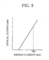
- FIG. 9 shows a current-optical output characteristic curve for this device.
- the semiconductor laser device of the gain-waveguide type according to the present invention undergoes longitudinal multi-mode oscillation.
- the module that is formed by connecting the device to the optical fiber therefore, a bad influence of the return light can be restrained, and there is no possibility of dislocation of transverse modes (beam steering) in a far field pattern, so that fluctuations of the fetched optical output can be inhibited.
- the linearity of the current-optical output characteristic can be maintained as a whole even if the injected current is increased.
- the device according to the present invention for use as a pumping light source for optical fiber amplifier, is of great industrial value.
Landscapes
- Physics & Mathematics (AREA)
- Condensed Matter Physics & Semiconductors (AREA)
- General Physics & Mathematics (AREA)
- Electromagnetism (AREA)
- Optics & Photonics (AREA)
- Semiconductor Lasers (AREA)
Abstract
Description
Claims (5)
- A semiconductor laser device comprising:a laminated structure of a semiconductor material including an active layer formed of a quantum well structure;a low-reflection film formed on one end face of the structure;a high-reflection film formed on the other end face of the structure; andthe cavity length of the device being 1,200 µm or more.
- The semiconductor laser device according to claim 1, wherein said device has a transverse light confinement structure with the transverse refractive index difference of about 1 x 10⁻² or less for oscillation modes.
- The semiconductor laser device according to claim 1, wherein the reflectance of said low-reflection film on the one end face is 5% or less.
- The semiconductor laser device according to claim 1, wherein said active layer is formed of one or two quantum well structures.
- The semiconductor laser device according to any one of claims 1 to 4, wherein the coefficient of light confinement to the active layer ranges from 1% to 2%.
Applications Claiming Priority (3)
| Application Number | Priority Date | Filing Date | Title |
|---|---|---|---|
| JP16279299 | 1999-06-09 | ||
| JP16279299 | 1999-06-09 | ||
| PCT/JP2000/002881 WO2000076041A1 (en) | 1999-06-09 | 2000-05-01 | Semiconductor laser |
Publications (3)
| Publication Number | Publication Date |
|---|---|
| EP1104054A1 true EP1104054A1 (en) | 2001-05-30 |
| EP1104054A4 EP1104054A4 (en) | 2006-06-21 |
| EP1104054B1 EP1104054B1 (en) | 2013-04-10 |
Family
ID=15761305
Family Applications (1)
| Application Number | Title | Priority Date | Filing Date |
|---|---|---|---|
| EP00922939.4A Expired - Lifetime EP1104054B1 (en) | 1999-06-09 | 2000-05-01 | Semiconductor laser |
Country Status (4)
| Country | Link |
|---|---|
| US (1) | US6810063B1 (en) |
| EP (1) | EP1104054B1 (en) |
| CA (1) | CA2339955A1 (en) |
| WO (1) | WO2000076041A1 (en) |
Cited By (1)
| Publication number | Priority date | Publication date | Assignee | Title |
|---|---|---|---|---|
| DE10260378A1 (en) * | 2002-12-16 | 2004-07-08 | Infineon Technologies Ag | Optoelectronic component for generating short light pulses has active coating on semiconducting substrate associated with amplifier, further active coating on substrate associated with absorber |
Family Cites Families (49)
| Publication number | Priority date | Publication date | Assignee | Title |
|---|---|---|---|---|
| US4616898A (en) | 1980-03-31 | 1986-10-14 | Polaroid Corporation | Optical communication systems using raman repeaters and components therefor |
| JPS5814590A (en) * | 1981-07-17 | 1983-01-27 | Matsushita Electric Ind Co Ltd | Semiconductor laser |
| US4731792A (en) * | 1983-06-29 | 1988-03-15 | Matsushita Electric Industrial Co., Ltd. | Semiconductor laser device with decreased light intensity noise |
| JPS62276892A (en) | 1986-05-26 | 1987-12-01 | Hitachi Ltd | electronic components |
| US5377291A (en) * | 1989-01-13 | 1994-12-27 | Kabushiki Kaisha Toshiba | Wavelength converting optical device |
| JP2884603B2 (en) | 1989-07-17 | 1999-04-19 | 住友電気工業株式会社 | Semiconductor laser device |
| RO102871B1 (en) * | 1990-04-20 | 1993-08-16 | Inst De Fizica Si Tehnologia M | High power laser diode |
| JPH05206580A (en) | 1991-05-17 | 1993-08-13 | Canon Inc | External-cavity laser device |
| JPH05206579A (en) | 1991-05-17 | 1993-08-13 | Canon Inc | External-cavity laser device |
| JP3149965B2 (en) | 1991-05-21 | 2001-03-26 | 日本電気株式会社 | Optical semiconductor module |
| US5189679A (en) | 1991-09-06 | 1993-02-23 | The Boeing Company | Strained quantum well laser for high temperature operation |
| JPH05136511A (en) | 1991-11-15 | 1993-06-01 | Sumitomo Electric Ind Ltd | Optical fiber amplifier |
| US5305336A (en) | 1992-01-29 | 1994-04-19 | At&T Bell Laboratories | Compact optical pulse source |
| JPH05315705A (en) | 1992-05-08 | 1993-11-26 | Nec Corp | Semiconductor laser device |
| JPH05327031A (en) | 1992-05-22 | 1993-12-10 | Fujitsu Ltd | Optical semiconductor module |
| JP3326283B2 (en) | 1993-08-05 | 2002-09-17 | シャープ株式会社 | Semiconductor laser device |
| US5563732A (en) | 1994-01-06 | 1996-10-08 | At&T Corp. | Laser pumping of erbium amplifier |
| KR100357787B1 (en) * | 1994-01-31 | 2003-01-24 | 가부시끼가이샤 히다치 세이사꾸쇼 | Manufacturing method of waveguide fluorescent element |
| DE69517614T2 (en) * | 1994-03-22 | 2001-02-15 | Uniphase Opto Holdings Inc., San Jose | Semiconductor diode laser and its manufacturing process |
| JP3596029B2 (en) | 1994-06-06 | 2004-12-02 | 住友電気工業株式会社 | Semiconductor laser module |
| JPH08116124A (en) | 1994-10-13 | 1996-05-07 | Hitachi Ltd | Semiconductor optical device |
| JPH08201609A (en) | 1995-01-23 | 1996-08-09 | Fujikura Ltd | Chirped fiber grating |
| JPH08330671A (en) | 1995-05-31 | 1996-12-13 | Hitachi Ltd | Semiconductor optical device |
| JP3987138B2 (en) | 1995-07-11 | 2007-10-03 | 三井化学株式会社 | Semiconductor laser element |
| JPH0983059A (en) | 1995-09-08 | 1997-03-28 | Nippon Telegr & Teleph Corp <Ntt> | Semiconductor laser |
| US5978401A (en) * | 1995-10-25 | 1999-11-02 | Honeywell Inc. | Monolithic vertical cavity surface emitting laser and resonant cavity photodetector transceiver |
| JPH09219475A (en) | 1996-02-09 | 1997-08-19 | Hitachi Denshi Ltd | Electric cooling element power supply circuit |
| US5724377A (en) | 1996-02-29 | 1998-03-03 | Lucent Technologies Inc. | Method and apparatus for improving the instability of a laser |
| JPH09260766A (en) | 1996-03-19 | 1997-10-03 | Matsushita Electric Ind Co Ltd | Semiconductor laser and method of manufacturing the same |
| TW342545B (en) * | 1996-03-28 | 1998-10-11 | Sanyo Electric Co | Semiconductor laser element and method for designing same |
| JP3754169B2 (en) | 1996-03-28 | 2006-03-08 | 三洋電機株式会社 | Semiconductor laser device and design method thereof |
| JP2828025B2 (en) | 1996-03-29 | 1998-11-25 | 日本電気株式会社 | Semiconductor laser module |
| JPH09275240A (en) | 1996-04-02 | 1997-10-21 | Hitachi Ltd | Waveguide optical element and method of manufacturing the same |
| JP3120828B2 (en) | 1996-04-08 | 2000-12-25 | 住友電気工業株式会社 | Semiconductor laser module |
| US5699377A (en) | 1996-04-30 | 1997-12-16 | E-Tek Dynamics, Inc. | Narrow linewidth, stabilized semiconductor laser source |
| JP3560414B2 (en) | 1996-05-07 | 2004-09-02 | 北川工業株式会社 | Peltier element |
| JPH1012959A (en) | 1996-06-19 | 1998-01-16 | Sumitomo Electric Ind Ltd | Semiconductor light emitting device, light emitting device module, and method of manufacturing semiconductor light emitting device |
| JPH1062654A (en) | 1996-08-15 | 1998-03-06 | Furukawa Electric Co Ltd:The | Semiconductor laser module |
| US5936763A (en) | 1996-11-15 | 1999-08-10 | Matsushita Electric Industrial Co., Ltd. | Optical fiber amplifier, semiconductor laser module for pumping and optical signal communication system |
| US5870417A (en) * | 1996-12-20 | 1999-02-09 | Sdl, Inc. | Thermal compensators for waveguide DBR laser sources |
| US5801403A (en) | 1997-04-04 | 1998-09-01 | Opto Power Corporation | Low divergence laser diode |
| JPH1117248A (en) | 1997-06-25 | 1999-01-22 | Nippon Telegr & Teleph Corp <Ntt> | Highly reflective film structure for semiconductor laser and semiconductor laser |
| EP0898345A3 (en) * | 1997-08-13 | 2004-01-02 | Mitsubishi Chemical Corporation | Compound semiconductor light emitting device and method of fabricating the same |
| US6122299A (en) * | 1997-12-31 | 2000-09-19 | Sdl, Inc. | Angled distributed reflector optical device with enhanced light confinement |
| US6396861B1 (en) * | 1999-01-11 | 2002-05-28 | The Furukawa Electric Co., Ltd. | N-type modulation-doped multi quantum well semiconductor laser device |
| EP1069659A4 (en) * | 1999-02-03 | 2003-03-05 | Furukawa Electric Co Ltd | Semiconductor laser and semiconductor laser module using the same |
| US6614822B2 (en) * | 2000-02-03 | 2003-09-02 | The Furukawa Electric Co., Ltd. | Semiconductor laser devices, and semiconductor laser modules and optical communication systems using the same |
| US6738403B2 (en) * | 2000-04-06 | 2004-05-18 | Fuji Photo Film Co., Ltd. | Semiconductor laser element and semiconductor laser |
| JP2003115634A (en) * | 2001-08-02 | 2003-04-18 | Furukawa Electric Co Ltd:The | Surface emitting laser device |
-
2000
- 2000-02-25 US US09/513,702 patent/US6810063B1/en not_active Expired - Lifetime
- 2000-05-01 WO PCT/JP2000/002881 patent/WO2000076041A1/en not_active Ceased
- 2000-05-01 EP EP00922939.4A patent/EP1104054B1/en not_active Expired - Lifetime
- 2000-05-01 CA CA002339955A patent/CA2339955A1/en not_active Abandoned
Cited By (1)
| Publication number | Priority date | Publication date | Assignee | Title |
|---|---|---|---|---|
| DE10260378A1 (en) * | 2002-12-16 | 2004-07-08 | Infineon Technologies Ag | Optoelectronic component for generating short light pulses has active coating on semiconducting substrate associated with amplifier, further active coating on substrate associated with absorber |
Also Published As
| Publication number | Publication date |
|---|---|
| CA2339955A1 (en) | 2000-12-14 |
| EP1104054A4 (en) | 2006-06-21 |
| EP1104054B1 (en) | 2013-04-10 |
| WO2000076041A1 (en) | 2000-12-14 |
| US6810063B1 (en) | 2004-10-26 |
Similar Documents
| Publication | Publication Date | Title |
|---|---|---|
| US6014396A (en) | Flared semiconductor optoelectronic device | |
| Sebastian et al. | High-power 810-nm GaAsP-AlGaAs diode lasers with narrow beam divergence | |
| US6594297B1 (en) | Laser apparatus in which surface-emitting semiconductor is excited with semiconduct laser element and high-order oscillation modes are suppressed | |
| Koyama et al. | Multiple-quantum-well GaInAs/GaInAsP tapered broad-area amplifiers with monolithically integrated waveguide lens for high-power applications | |
| CA2473396C (en) | High coherent power, two-dimensional surface-emitting semiconductor diode array laser | |
| JP3322512B2 (en) | Design method of semiconductor laser device | |
| Mikulla | Tapered high-power, high-brightness diode lasers: design and performance | |
| US5953358A (en) | Semiconductor laser device | |
| US7072373B2 (en) | Ridge waveguide semiconductor laser diode | |
| Gao et al. | High-power highly reliable single emitter laser diodes at 808 nm | |
| Walker et al. | A gain-clamped, crosstalk free, vertical cavity lasing semiconductor optical amplifier for WDM applications | |
| US6810063B1 (en) | Semiconductor laser device | |
| Ostendorf et al. | 10 W high-efficiency high-brightness tapered diode lasers at 976 nm | |
| US20010021212A1 (en) | Fundamental-transverse-mode index-guided semiconductor laser device having upper optical waveguide layer thicker than lower optical waveguide layer | |
| CA1318722C (en) | Surface emitting lasers with combined output | |
| JP4297322B2 (en) | Semiconductor laser device and laser module using the same | |
| JPH10209553A (en) | Semiconductor laser device | |
| CN100397734C (en) | laser components | |
| JPH0671121B2 (en) | Semiconductor laser device | |
| JP3606933B2 (en) | Semiconductor laser | |
| EP0144205B1 (en) | Semiconductor laser | |
| US6738405B1 (en) | Semiconductor laser | |
| Liou et al. | Single-quantum-well strained-layer InGaAs-InGaAsP lasers for the wavelength range from 1.43 to 1.55 mu m | |
| JP2001148541A (en) | Semiconductor light emitting device and solid-state laser device using the semiconductor light emitting device as excitation light source | |
| Friedmann et al. | 5 W frequency stabilized 976 nm tapered diode lasers |
Legal Events
| Date | Code | Title | Description |
|---|---|---|---|
| PUAI | Public reference made under article 153(3) epc to a published international application that has entered the european phase |
Free format text: ORIGINAL CODE: 0009012 |
|
| 17P | Request for examination filed |
Effective date: 20010206 |
|
| AK | Designated contracting states |
Kind code of ref document: A1 Designated state(s): AT BE CH CY DE DK ES FI FR GB GR IE IT LI LU MC NL PT SE |
|
| RBV | Designated contracting states (corrected) |
Designated state(s): CH DE FR GB IT LI |
|
| A4 | Supplementary search report drawn up and despatched |
Effective date: 20060524 |
|
| 17Q | First examination report despatched |
Effective date: 20080904 |
|
| GRAP | Despatch of communication of intention to grant a patent |
Free format text: ORIGINAL CODE: EPIDOSNIGR1 |
|
| GRAS | Grant fee paid |
Free format text: ORIGINAL CODE: EPIDOSNIGR3 |
|
| GRAA | (expected) grant |
Free format text: ORIGINAL CODE: 0009210 |
|
| AK | Designated contracting states |
Kind code of ref document: B1 Designated state(s): CH DE FR GB IT LI |
|
| REG | Reference to a national code |
Ref country code: GB Ref legal event code: FG4D |
|
| REG | Reference to a national code |
Ref country code: CH Ref legal event code: EP |
|
| REG | Reference to a national code |
Ref country code: DE Ref legal event code: R096 Ref document number: 60047945 Country of ref document: DE Effective date: 20130606 |
|
| REG | Reference to a national code |
Ref country code: CH Ref legal event code: NV Representative=s name: ISLER AND PEDRAZZINI AG, CH |
|
| PG25 | Lapsed in a contracting state [announced via postgrant information from national office to epo] |
Ref country code: DE Free format text: LAPSE BECAUSE OF NON-PAYMENT OF DUE FEES Effective date: 20131203 |
|
| PLBE | No opposition filed within time limit |
Free format text: ORIGINAL CODE: 0009261 |
|
| STAA | Information on the status of an ep patent application or granted ep patent |
Free format text: STATUS: NO OPPOSITION FILED WITHIN TIME LIMIT |
|
| REG | Reference to a national code |
Ref country code: DE Ref legal event code: R119 Ref document number: 60047945 Country of ref document: DE Effective date: 20131203 |
|
| PG25 | Lapsed in a contracting state [announced via postgrant information from national office to epo] |
Ref country code: IT Free format text: LAPSE BECAUSE OF FAILURE TO SUBMIT A TRANSLATION OF THE DESCRIPTION OR TO PAY THE FEE WITHIN THE PRESCRIBED TIME-LIMIT Effective date: 20130410 |
|
| REG | Reference to a national code |
Ref country code: FR Ref legal event code: ST Effective date: 20140131 |
|
| 26N | No opposition filed |
Effective date: 20140113 |
|
| GBPC | Gb: european patent ceased through non-payment of renewal fee |
Effective date: 20130710 |
|
| PG25 | Lapsed in a contracting state [announced via postgrant information from national office to epo] |
Ref country code: GB Free format text: LAPSE BECAUSE OF NON-PAYMENT OF DUE FEES Effective date: 20130710 |
|
| PG25 | Lapsed in a contracting state [announced via postgrant information from national office to epo] |
Ref country code: FR Free format text: LAPSE BECAUSE OF NON-PAYMENT OF DUE FEES Effective date: 20130610 |
|
| PGFP | Annual fee paid to national office [announced via postgrant information from national office to epo] |
Ref country code: CH Payment date: 20160511 Year of fee payment: 17 |
|
| REG | Reference to a national code |
Ref country code: CH Ref legal event code: PL |
|
| PG25 | Lapsed in a contracting state [announced via postgrant information from national office to epo] |
Ref country code: LI Free format text: LAPSE BECAUSE OF NON-PAYMENT OF DUE FEES Effective date: 20170531 Ref country code: CH Free format text: LAPSE BECAUSE OF NON-PAYMENT OF DUE FEES Effective date: 20170531 |