EP1104030A2 - Manufacturing method of photovoltaic device - Google Patents
Manufacturing method of photovoltaic device Download PDFInfo
- Publication number
- EP1104030A2 EP1104030A2 EP00126006A EP00126006A EP1104030A2 EP 1104030 A2 EP1104030 A2 EP 1104030A2 EP 00126006 A EP00126006 A EP 00126006A EP 00126006 A EP00126006 A EP 00126006A EP 1104030 A2 EP1104030 A2 EP 1104030A2
- Authority
- EP
- European Patent Office
- Prior art keywords
- zinc oxide
- etching
- substrate
- photovoltaic device
- oxide film
- Prior art date
- Legal status (The legal status is an assumption and is not a legal conclusion. Google has not performed a legal analysis and makes no representation as to the accuracy of the status listed.)
- Withdrawn
Links
- 238000004519 manufacturing process Methods 0.000 title claims abstract description 27
- XLOMVQKBTHCTTD-UHFFFAOYSA-N Zinc monoxide Chemical compound [Zn]=O XLOMVQKBTHCTTD-UHFFFAOYSA-N 0.000 claims abstract description 140
- 239000000758 substrate Substances 0.000 claims abstract description 82
- 239000011787 zinc oxide Substances 0.000 claims abstract description 70
- 238000000034 method Methods 0.000 claims abstract description 42
- 238000005530 etching Methods 0.000 claims abstract description 36
- 238000006243 chemical reaction Methods 0.000 claims abstract description 21
- 239000011521 glass Substances 0.000 claims description 39
- 238000001039 wet etching Methods 0.000 claims description 4
- 238000001312 dry etching Methods 0.000 claims description 3
- 239000002253 acid Substances 0.000 claims 2
- 229910052736 halogen Inorganic materials 0.000 claims 2
- 150000002367 halogens Chemical class 0.000 claims 2
- 239000007787 solid Substances 0.000 claims 2
- 239000010408 film Substances 0.000 description 80
- 239000010410 layer Substances 0.000 description 32
- 229910021417 amorphous silicon Inorganic materials 0.000 description 18
- 239000004065 semiconductor Substances 0.000 description 18
- 239000000463 material Substances 0.000 description 17
- XOLBLPGZBRYERU-UHFFFAOYSA-N tin dioxide Chemical compound O=[Sn]=O XOLBLPGZBRYERU-UHFFFAOYSA-N 0.000 description 16
- 238000012545 processing Methods 0.000 description 13
- 238000009792 diffusion process Methods 0.000 description 10
- 229910052751 metal Inorganic materials 0.000 description 9
- 239000002184 metal Substances 0.000 description 9
- 238000004544 sputter deposition Methods 0.000 description 9
- 230000015556 catabolic process Effects 0.000 description 8
- 238000006731 degradation reaction Methods 0.000 description 8
- BLRPTPMANUNPDV-UHFFFAOYSA-N Silane Chemical compound [SiH4] BLRPTPMANUNPDV-UHFFFAOYSA-N 0.000 description 6
- ZAMOUSCENKQFHK-UHFFFAOYSA-N Chlorine atom Chemical compound [Cl] ZAMOUSCENKQFHK-UHFFFAOYSA-N 0.000 description 5
- 229910052801 chlorine Inorganic materials 0.000 description 5
- 239000000460 chlorine Substances 0.000 description 5
- 229910052782 aluminium Inorganic materials 0.000 description 4
- 230000015572 biosynthetic process Effects 0.000 description 4
- 230000000694 effects Effects 0.000 description 4
- 230000001788 irregular Effects 0.000 description 4
- 238000002844 melting Methods 0.000 description 4
- 230000008018 melting Effects 0.000 description 4
- 230000002787 reinforcement Effects 0.000 description 4
- HBMJWWWQQXIZIP-UHFFFAOYSA-N silicon carbide Chemical compound [Si+]#[C-] HBMJWWWQQXIZIP-UHFFFAOYSA-N 0.000 description 4
- 239000002904 solvent Substances 0.000 description 4
- 229910001887 tin oxide Inorganic materials 0.000 description 4
- QTBSBXVTEAMEQO-UHFFFAOYSA-N Acetic acid Chemical compound CC(O)=O QTBSBXVTEAMEQO-UHFFFAOYSA-N 0.000 description 3
- LEVVHYCKPQWKOP-UHFFFAOYSA-N [Si].[Ge] Chemical compound [Si].[Ge] LEVVHYCKPQWKOP-UHFFFAOYSA-N 0.000 description 3
- 239000005357 flat glass Substances 0.000 description 3
- 239000007789 gas Substances 0.000 description 3
- 229910021424 microcrystalline silicon Inorganic materials 0.000 description 3
- 238000000926 separation method Methods 0.000 description 3
- 229910052709 silver Inorganic materials 0.000 description 3
- XLYOFNOQVPJJNP-UHFFFAOYSA-N water Substances O XLYOFNOQVPJJNP-UHFFFAOYSA-N 0.000 description 3
- 229910052733 gallium Inorganic materials 0.000 description 2
- 229910010272 inorganic material Inorganic materials 0.000 description 2
- 239000011147 inorganic material Substances 0.000 description 2
- 238000009413 insulation Methods 0.000 description 2
- 229910052749 magnesium Inorganic materials 0.000 description 2
- 238000005259 measurement Methods 0.000 description 2
- 238000005268 plasma chemical vapour deposition Methods 0.000 description 2
- 239000004332 silver Substances 0.000 description 2
- 239000010409 thin film Substances 0.000 description 2
- 229910001218 Gallium arsenide Inorganic materials 0.000 description 1
- XUIMIQQOPSSXEZ-UHFFFAOYSA-N Silicon Chemical compound [Si] XUIMIQQOPSSXEZ-UHFFFAOYSA-N 0.000 description 1
- XAGFODPZIPBFFR-UHFFFAOYSA-N aluminium Chemical compound [Al] XAGFODPZIPBFFR-UHFFFAOYSA-N 0.000 description 1
- PNEYBMLMFCGWSK-UHFFFAOYSA-N aluminium oxide Inorganic materials [O-2].[O-2].[O-2].[Al+3].[Al+3] PNEYBMLMFCGWSK-UHFFFAOYSA-N 0.000 description 1
- 239000011248 coating agent Substances 0.000 description 1
- 238000000576 coating method Methods 0.000 description 1
- 150000001875 compounds Chemical class 0.000 description 1
- 229910052593 corundum Inorganic materials 0.000 description 1
- 229910021419 crystalline silicon Inorganic materials 0.000 description 1
- 230000007423 decrease Effects 0.000 description 1
- 238000011161 development Methods 0.000 description 1
- 230000005611 electricity Effects 0.000 description 1
- 238000002474 experimental method Methods 0.000 description 1
- 238000007499 fusion processing Methods 0.000 description 1
- QUZPNFFHZPRKJD-UHFFFAOYSA-N germane Chemical compound [GeH4] QUZPNFFHZPRKJD-UHFFFAOYSA-N 0.000 description 1
- 229910052986 germanium hydride Inorganic materials 0.000 description 1
- 239000011810 insulating material Substances 0.000 description 1
- 230000001678 irradiating effect Effects 0.000 description 1
- 238000003475 lamination Methods 0.000 description 1
- 238000002488 metal-organic chemical vapour deposition Methods 0.000 description 1
- 229910021420 polycrystalline silicon Inorganic materials 0.000 description 1
- 229920001296 polysiloxane Polymers 0.000 description 1
- 239000012495 reaction gas Substances 0.000 description 1
- 230000003014 reinforcing effect Effects 0.000 description 1
- 229910052710 silicon Inorganic materials 0.000 description 1
- 239000010703 silicon Substances 0.000 description 1
- 239000002356 single layer Substances 0.000 description 1
- 229910001845 yogo sapphire Inorganic materials 0.000 description 1
Images

Classifications
-
- H—ELECTRICITY
- H01—ELECTRIC ELEMENTS
- H01L—SEMICONDUCTOR DEVICES NOT COVERED BY CLASS H10
- H01L31/00—Semiconductor devices sensitive to infrared radiation, light, electromagnetic radiation of shorter wavelength or corpuscular radiation and specially adapted either for the conversion of the energy of such radiation into electrical energy or for the control of electrical energy by such radiation; Processes or apparatus specially adapted for the manufacture or treatment thereof or of parts thereof; Details thereof
- H01L31/02—Details
- H01L31/0224—Electrodes
-
- H—ELECTRICITY
- H01—ELECTRIC ELEMENTS
- H01L—SEMICONDUCTOR DEVICES NOT COVERED BY CLASS H10
- H01L31/00—Semiconductor devices sensitive to infrared radiation, light, electromagnetic radiation of shorter wavelength or corpuscular radiation and specially adapted either for the conversion of the energy of such radiation into electrical energy or for the control of electrical energy by such radiation; Processes or apparatus specially adapted for the manufacture or treatment thereof or of parts thereof; Details thereof
- H01L31/18—Processes or apparatus specially adapted for the manufacture or treatment of these devices or of parts thereof
-
- Y—GENERAL TAGGING OF NEW TECHNOLOGICAL DEVELOPMENTS; GENERAL TAGGING OF CROSS-SECTIONAL TECHNOLOGIES SPANNING OVER SEVERAL SECTIONS OF THE IPC; TECHNICAL SUBJECTS COVERED BY FORMER USPC CROSS-REFERENCE ART COLLECTIONS [XRACs] AND DIGESTS
- Y10—TECHNICAL SUBJECTS COVERED BY FORMER USPC
- Y10S—TECHNICAL SUBJECTS COVERED BY FORMER USPC CROSS-REFERENCE ART COLLECTIONS [XRACs] AND DIGESTS
- Y10S438/00—Semiconductor device manufacturing: process
- Y10S438/94—Laser ablative material removal
Definitions
- This invention relates to an integrated photovoltaic device, particularly relates to a manufacturing method of a photovoltaic device provided with a transparent electrode of zinc oxide.
- a photovoltaic device such as a solar cell can directly convert sunlight into electricity and has been commercialized as a new energy source.
- Such the photovoltaic device has been formed of crystalline semiconductor material such as single crystalline silicon and polycrystalline silicon, compound semiconductor material such as GaAs, InP or the like, and amorphous semiconductor material such as amorphous silicon and amorphous silicon germanium or the like.
- the photovoltaic device using the amorphous semiconductor material is manufactured at a low temperature as compared with other semiconductor material, can increase a size easily, and can easily be integrated on a substrate.
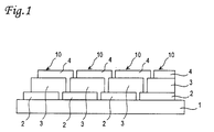
- Fig. 1 is a structural cross sectional view of an integrated photovoltaic device using the amorphous semiconductor material.
- a substrate 1 is formed of translucent and insulating material such as glass, plastic, or the like.
- a plurality of first electrodes 2 are arranged on a surface of the substrate 1.
- the first electrode 2 is formed of tin oxide (SnO 2 ) and has a rough plane for scattering light incident from the substrate 1 on the surface. This rough plane is generally referred as a texture plane.
- a photovoltaic conversion layer 3 is formed of amorphous semiconductor material, and generally includes a p-type amorphous silicon carbide film of approximately 100 ⁇ , an intrinsic amorphous silicon film of approximately 4000 A, and an n-type amorphous silicon film of approximately 200 ⁇ laminated in this order from a side of the first electrode 2.
- a second electrode 4 is formed of a highly reflective metal film such as Ag, Al or the like.
- a lamination body of the first electrode 2, the photovoltaic conversion layer 3, and the second electrode 4 is a unit cell 10, and adjacent unit cells 10 are electrically connected in series by electrically linking the first electrode 2 of the one unit cell 10 and the second electrode 4 of the other unit cell 10.
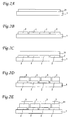
- Figs. 2A-2E are structural cross sectional views of each of processes for illustrating manufacturing processes of the conventional photovoltaic device.
- a transparent electrode film 21 of tin oxide (SnO 2 ) having a texture plane is formed on a surface of the substrate 1.
- a predetermined part of the transparent electrode film 21 is eliminated by laser beam irradiation and is divided into a plurality of the first electrodes 2, as shown in Fig. 2B.
- An amorphous semiconductor film 31 having pin junction inside is formed on the substrate so as to cover over the first electrodes 2 as shown in Fig. 2C.
- a predetermined part of the amorphous semiconductor film 31 is eliminated by laser beam irradiation and is divided into a plurality of the photovoltaic conversion layers 3 as shown in Fig. 2D.
- a metal film 4 is formed on the substrate 1 so as to cover the photovoltaic conversion layers 3 as shown in Fig. 2E. Then, a predetermined part of the metal film 41 is eliminated by laser beam irradiation and is divided into a plurality of the second electrodes 4 to produce the photovoltaic device as shown in Fig. 1.
- the material for forming the first electrode as the transparent electrode is conventionally SnO 2 .
- SnO 2 requires a temperature higher than approximately 500°C, resulting in an increase in manufacture cost.
- a substrate of less heat resistance such as plastic can not be usable and selection of substrate material is limited.
- the first electrode of zinc oxide can be prepared at a low temperature of not higher than 200°C by sputtering, resulting in reduction of manufacture cost.
- selection of the substrate material is not limited as tightly as in the conventional case.
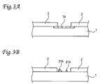
- the applicants of this invention have examined and found that it is more difficult to electrically separate the adjacent first electrodes of zinc oxide in eliminating the predetermined part of the zinc oxide film by laser beam irradiation and dividing into a plurality of the first electrodes as compared with the first electrode of a SnO 2 film. Thus, leak current is likely to occur between adjacent unit cells of the photovoltaic device comprising the first electrodes of zinc oxide and the photovoltaic conversion characteristics are degraded.
- the first electrode is formed of zinc oxide and intensity of laser beams to be irradiated is great, doping material of Al, Mg, Ga or the like included in the zinc oxide is scattered and the diffusion region is formed on a surface of the substrate.
- the intensity of the laser beams is small, residual of zinc oxide is generated. In these cases, it is expected that leak current occurs between the adjacent first electrodes through the diffusion region and the residual, and photovoltaic conversion characteristic are degraded.
- the energy beams In processing the transparent electrode by energy beams, the energy beams should be applied so that the temperature increases momentarily up to approximately 2000°C of a melting point. Therefore, heat from irradiation energy transmits to a side of the glass when the energy beams are irradiated in order to divide the transparent electrode into a plurality of regions even though the transparent electrode of good characteristics are formed at lower than 500°C. As a result, the temperature increases up to higher than 500°C locally, which causes fine cracks and irregular degradation of strength of the part of the glass to degrade the strength of the entire glass.
- This invention was made to solve the existing problem and provides a manufacturing method of a photovoltaic device comprising a first electrode of zinc oxide capable of improving photovoltaic conversion characteristics.
- This invention provides a manufacturing method capable of using reinforced glass as a substrate, improving photovoltaic conversion characteristic, and having sufficient mechanical strength
- a manufacturing method of a photovoltaic device provided with a plurality of unit cells including a first electrode of zinc oxide, a photovoltaic conversion layer, and a second electrode on a surface of a transparent substrate comprises a process for forming a zinc oxide film on a surface of a substrate, a process for eliminating a predetermined part of the zinc oxide film by energy beam irradiation and dividing the zinc oxide film into a plurality of the first electrodes, and a process for etching the surface of the substrate provided with the plurality of the first electrodes.
- a texture plane is formed on a surface of the first electrode by etching.
- a predetermined part of the zinc oxide film is eliminated by energy beam irradiation and the zinc oxide film is divided into a plurality of the first electrodes. Then, a diffusion region and residual of zinc oxide formed on a surface of the substrate are eliminated by etching. Leak current between the adjacent first electrodes decreases greatly as compared with the conventional case. Therefore, a photovoltaic device with excellent photovoltaic conversion characteristics can be provided by this invention.
- a manufacturing method of a photovoltaic device provided with a plurality of unit cells including a first electrode of zinc oxide, a photovoltaic conversion layer, and a second electrode on a surface of a transparent substrate comprising a process for forming a zinc oxide film on a surface of a substrate, a process for eliminating a predetermined part of the zinc oxide film by energy beam irradiation so as to leave the zinc oxide film of not less than a predetermined thickness on a side of the transparent substrate and preliminarily dividing the zinc oxide film into a plurality of the first electrodes, and a process for etching the surface of the substrate provided with the plurality of the first electrodes which are preliminarily divided, and electrically separating adjacent divided areas.
- the transparent substrate is a reinforced glass.
- the transparent electrode of more than a predetermined thickness is intentionally remained on a glass substrate side of the transparent electrode in a process for dividing into a plurality of regions by energy beams, and the adjacent divided regions are electrically separated in the etching process. Degradation of substrate strength caused by fine cracks and irregular degradation of strength caused by heat transmitted to the glass in processing the transparent electrodes by energy beams is prevented with these processes.
- the above second constitution prevents an increase of a temperature to a melting point of glass and maintains an effect of reinforcement, thus is particularly effective in using reinforced glass.
- a zinc oxide film 21 is formed on a substrate 1 by sputtering.
- a predetermined part of the zinc oxide film 21 is eliminated by laser beam irradiation and is divided into a plurality of the first electrodes 2.
- a diffusion region 1A on the substrate 1 and residual 21A of the zinc oxide film seem to be generated, as shown in Figs. 3A-3B.
- the surface of the substrate 1 provided with a plurality of the divided first electrodes 2 is etched. By this etching, the residual 21A of zinc oxide and the diffusion region 1A are eliminated.
- the etching may be dry etching or wet etching; any of methods capable of eliminating the diffusion region 1A on the substrate 1 and the residual 21A of zinc oxide. To eliminate them, selection of etching gas or etching solvent is important. It is required to select etching gas or etching solvent capable of etching component of the substrate 1 and zinc oxide. For example, chlorine solvent and acetic acid solvent are preferred for wet etching, but any one capable of etching component of the substrate 1 and zinc oxide can be used.
- a p-type amorphous silicon carbide film of approximately 100 ⁇ , an intrinsic amorphous silicon film of approximately 4000 ⁇ , and an n-type amorphous silicon film of approximately 200 ⁇ are laminated in this order on the substrate 1 so as to cover the etched first electrodes 2 to form an amorphous semiconductor film 31.
- a predetermined part of the amorphous semiconductor film 31 is eliminated by laser beam irradiation and is divided into a plurality of photovoltaic conversion layers 3.
- a metal film 41 of silver is formed on the substrate 1 so as to cover the photovoltaic conversion layers 3 by sputtering. Then, a predetermined part of the metal film 41 is eliminated by laser beam irradiation and is divided into a plurality of the second electrodes 4 to manufacture an integrated photovoltaic device.
- the diffusion region 1A on the substrate 1 and the residual 21A of zinc oxide are eliminated. Therefore, leak current between the adjacent first electrodes is greatly reduced as compared with the conventional case, and a photovoltaic device having excellent photovoltaic characteristics is produced in this invention.
- a glass substrate is prepared as the substrate 1.
- a size of the substrate is 30 ⁇ 40cm and 5mm in thickness.
- the zinc oxide film 21 of approximately 1 ⁇ m is formed on an approximately entire surface of the substrate 1 by sputtering.
- Conditions for forming the zinc oxide film is shown in Table 1.
- Target ZnO Al 2 O 3 dope : 2 wt.%)
- Applied RF power 400W Pressure
- 13.33Pa Sputtering gas Ar 20SCCM
- a predetermined part of the zinc oxide film 21 is eliminated by irradiation of YAG laser beam of wavelength 1.06 ⁇ m, pulse frequency 3kHz, and intensity 4.0 ⁇ 10 7 W/cm 2 , and is divided into a plurality of the first electrodes 2.
- the zinc oxide film 21 is not completely eliminated by the YAG laser beam irradiation under these conditions, and the residual 21A of the zinc oxide film is found on the surface of the substrate 1.
- the substrate 1 having the plurality of the first electrodes 2 is immersed in chlorine solution of 0.5 wt.% for about 30 minutes, is etched, and is cleaned with pure water. By this etching, a texture plane is formed on the surface of the first electrode 2.
- a p-type amorphous silicon carbide layer of approximately 100 ⁇ , an intrinsic amorphous silicon layer of approximately 1500 ⁇ , a n-type microcrystalline silicon layer of approximately 200 ⁇ , a p-type amorphous silicone layer of approximately 100 ⁇ , an intrinsic amorphous silicon germanium layer of approximately 1000 ⁇ , and a n-type amorphous silicon layer of approximately 200 ⁇ are laminated in this order by plasma CVD so as to form an amorphous semiconductor film 31. Formation conditions of each of the layers are shown in Table 2. In this case, reaction pressure is controlled to be 50Pa.
- a predetermined part of the amorphous semiconductor film 31 is eliminated by irradiation of YAG laser beams of wavelength 1.06 ⁇ m, pulse frequency 3kHz, and intensity 1.3 ⁇ 10 8 W/cm 2 , and is divided into a plurality of photovoltaic conversion layers 3.
- a metal film 41 of silver of approximately 1 ⁇ m is formed on the substrate 1 by sputtering so as to cover the photovoltaic conversion layers 3, and a predetermined part of the metal film 41 is eliminated by irradiation of Ar laser beams of wavelength 0.51 ⁇ m and intensity 2 ⁇ 10 3 W/cm 2 , and is divided into a plurality of second electrodes 4 to produce a photovoltaic device of this embodiment.
- a photovoltaic device for comparison is manufactured by the same method as in the case of the first embodiment except for the etching process after division for forming the first electrodes 2.
- Table 3 shows measurement of a resistance value between the adjacent first electrodes 2 of the photovoltaic device of the embodiment and of the photovoltaic device of the comparison example.
- Table 4 shows measurement of the photovoltaic characteristics when light of AM1.5, 100mW/cm 2 is irradiated to the photovoltaic devices of the embodiment and the comparison example.
- this invention can produce a photovoltaic device having excellent photovoltaic characteristics as compared with the conventional one even when zinc oxide is used for the first electrode.
- the texture plane formed on the surface of the first electrode by the etching process after division for forming the first electrodes scatters incident light, leading to improved photovoltaic characteristics.
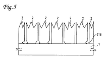
- the transparent electrode When the transparent electrode can not be electrically separated completely by scattered attachment generated in separating the transparent electrode by energy beams, a process such as etching or the like is effective for separation. At that time, as shown in Fig. 5, if a part 21B between the substrate 1 and the transparent electrode 2 which is readily etched is over-etched, the transparent electrode 2 in proximity of a part to be processed may be peeled, resulting in degraded reliability and characteristics of the device.
- a second embodiment provides a method for readily using reinforced glass and preventing over-etching.
- a reinforced glass substrate is used as a substrate 1.
- the size is 30 ⁇ 40cm, 5mm in thickness.
- a zinc oxide film 21 of 8000 ⁇ is formed on an approximately entire surface of the substrate 1 by sputtering. Conditions for forming the zinc oxide film are same as shown in Table 1.
- a predetermined part of the zinc oxide film 21 is processed with Nd:YAG laser of 1.06 ⁇ m wavelength, 3kHz pulse frequency, 2.0X 10 6 W/cm 2 laser power density, and 10mm/sec. processing rate to divide into a plurality of regions so as to form a photovoltaic device of 35-stage integrated connection.
- the dividing process by the YAG laser intentionally leaves the zinc oxide film 21C in a divided region.
- the zinc oxide film 21C of approximately 2000 ⁇ is intentionally left after processing.
- the substrate 1 processed with laser beams is immersed in chlorine solution of 1.0 wt.% for approximately 20 seconds and is etched to eliminate the remained zinc oxide film, and the substrate 1 is cleaned with pure water.
- a thickness of the zinc oxide film to be etched under the above conditions is approximately 2500 ⁇ .
- the remained zinc oxide film is eliminated and a plurality of the first electrodes 2 are formed.
- a texture plane on the surface of the first electrode 2 is formed.
- a cross section of the first electrode processed with energy beams is observed by a SEM with a magnification rate of 10,000. It was found from the observation that the residual of the zinc oxide film was eliminated from the processed part.
- the resistance value between the adjacent first electrodes 2 is measured by a tester, the value was more than 1M ⁇ and it was found that the electrodes were electrically separated.
- a p-type amorphous silicon carbide layer of approximately 100 ⁇ , an intrinsic amorphous silicon layer of approximately 1500 ⁇ , a n-type microcrystalline silicon layer of approximately 200 ⁇ , a p-type amorphous silicon layer of approximately 100 ⁇ , an intrinsic amorphous silicon germanium layer of approximately 1000 ⁇ , and a n-type amorphous silicon layer of approximately 200 ⁇ are laminated in this order by plasma CVD on the substrate 1 so as to cover the first electrodes 2 to form an amorphous semiconductor film 31.
- Conditions for forming each of the layers are same as shown in Table 2.
- YAG laser secondary harmonic of 0.53 ⁇ m wavelength, 3kHz pulse frequency is irradiated to a predetermined part of the amorphous semiconductor film 31 with 2X 10 7 W/cm 2 laser power density, 10mm/sec. processing rate for obtaining good workability, to divide into a plurality of photovoltaic conversion layers 3.
- a metal film 41 of aluminum of approximately 4000 ⁇ is formed on the substrate 1 so as to cover the photovoltaic conversion layers 3 by DC sputtering.
- This film is formed by applying power of 0.1kW to an A1 target of 300cm 2 under an atmosphere of Ar of 400sccm, 1Pa.
- YAG laser secondary harmonic of 0.53 ⁇ m wavelength, 3kHz pulse frequency is irradiated to a predetermined part of the metal film with 2 ⁇ 10 7 W/cm 2 laser power density, 10mm/sec. processing rate for obtaining good workability, to divide into a plurality of second electrodes. By these processes, the photovoltaic device of the second embodiment is produced.
- the predetermined part of the zinc oxide film 21 of approximately 8000 ⁇ is processed with Nd:YAG laser of 1.06 ⁇ m wavelength, 3kHz pulse frequency, 2.0 ⁇ 10 7 W/cm 2 laser power density, and 10mm/sec. processing rate to divide into a plurality of regions so as to form a photovoltaic device of 35 stage integrated connection.
- the substrate 1 processed with laser beams is immersed in chlorine solution of 1.0 wt.% for approximately 20 seconds and is etched. The remained zinc oxide film is eliminated, and the substrate 1 is cleaned with pure water.
- a photovoltaic device of the first embodiment is produced in the same way as in the second embodiment.
- F.F in the second embodiment improves as compared with the first embodiment.
- Table 6 compares an average breaking weight of a blue plate glass and a reinforced glass used in the first and second embodiments, wherein the parameter is 50. 2nd embodiment (reinforced) 1st embodiment (reinforced) 2nd embodiment (blue plate) 1st embodiment (blue plate) Average breaking weight (kgf) 2500 650 900 800
- a thickness of the film intentionally remained on the glass substrate of the transparent electrode is changed in the process for dividing into a plurality of regions by energy beams in the second embodiment. That is, in the process for dividing into a plurality of regions by energy beams, a thickness of the film intentionally remained on the transparent electrode is changed by controlling laser power and/or processing rate. Relative comparison is made on output of a solar cell using these substrates. In Table 7, laser power is changed and processing rate is made constant at 10mm/sec. The case of the thickness of remained film 2000 ⁇ is used as a reference. The film is etched by chlorine of 1 wt.% for 20 seconds. The thickness of the film to be etched is 2500 ⁇ in this case.
- a thickness to be remained is preferably 20-80% of the thickness to be etched.
- the transparent electrode of not less than a predetermined thickness is intentionally remained on a side of the glass substrate of the transparent electrode, and the adjacent divided regions are electrically separated in an etching process.
- the second embodiment is further effective in using a reinforced glass.
- a temperature of the reinforced glass increases to about 500°C, nearly at a glass fusing temperature, the reinforced glass is not effective. Therefore, the insulating film and the transparent conductive film are formed under a temperature not higher than 500°C.
- relatively good light transmittivity and conductivity can be obtained at not higher than 500°C particularly in using zinc oxide.
- zinc oxide formed by DC sputtering is used as the transparent electrode. This is because good film characteristics can be obtained at a relatively low substrate temperature 300 °C . If sufficient conductive characteristics can be obtained at a temperature not higher than around 500°C, other material such as tin oxide and other method of formation such as MOCVD are applicable.
- this embodiment does not form coating of insulating inorganic material on a surface of the glass substrate, the same effect can be obtained in a case of a glass substrate coated with the insulating inorganic material.
- this embodiment describes on an example of application to the integrated solar cell device of this invention, this invention can be applied to a pin single layer solar cell device.
- This invention can be applied not only to a solar cell but to a photovoltaic device such as a photo sensor or the like.
- YAG laser beams are used as energy beams for separating the transparent electrode
- line beams of excimer laser can be used for separation.
Abstract


Description
- This invention relates to an integrated photovoltaic device, particularly relates to a manufacturing method of a photovoltaic device provided with a transparent electrode of zinc oxide.
- A photovoltaic device such as a solar cell can directly convert sunlight into electricity and has been commercialized as a new energy source. Such the photovoltaic device has been formed of crystalline semiconductor material such as single crystalline silicon and polycrystalline silicon, compound semiconductor material such as GaAs, InP or the like, and amorphous semiconductor material such as amorphous silicon and amorphous silicon germanium or the like. The photovoltaic device using the amorphous semiconductor material is manufactured at a low temperature as compared with other semiconductor material, can increase a size easily, and can easily be integrated on a substrate.
- Fig. 1 is a structural cross sectional view of an integrated photovoltaic device using the amorphous semiconductor material.
- Explanation is made on the integrated photovoltaic device by referring to Fig. 1. A
substrate 1 is formed of translucent and insulating material such as glass, plastic, or the like. A plurality offirst electrodes 2 are arranged on a surface of thesubstrate 1. Thefirst electrode 2 is formed of tin oxide (SnO2) and has a rough plane for scattering light incident from thesubstrate 1 on the surface. This rough plane is generally referred as a texture plane. - A
photovoltaic conversion layer 3 is formed of amorphous semiconductor material, and generally includes a p-type amorphous silicon carbide film of approximately 100Å, an intrinsic amorphous silicon film of approximately 4000 A, and an n-type amorphous silicon film of approximately 200Å laminated in this order from a side of thefirst electrode 2. Asecond electrode 4 is formed of a highly reflective metal film such as Ag, Al or the like. - A lamination body of the
first electrode 2, thephotovoltaic conversion layer 3, and thesecond electrode 4 is aunit cell 10, andadjacent unit cells 10 are electrically connected in series by electrically linking thefirst electrode 2 of the oneunit cell 10 and thesecond electrode 4 of theother unit cell 10. - Figs. 2A-2E are structural cross sectional views of each of processes for illustrating manufacturing processes of the conventional photovoltaic device.
- As shown in Fig. 2A, a
transparent electrode film 21 of tin oxide (SnO2) having a texture plane is formed on a surface of thesubstrate 1. A predetermined part of thetransparent electrode film 21 is eliminated by laser beam irradiation and is divided into a plurality of thefirst electrodes 2, as shown in Fig. 2B. - An
amorphous semiconductor film 31 having pin junction inside is formed on the substrate so as to cover over thefirst electrodes 2 as shown in Fig. 2C. - Then, a predetermined part of the
amorphous semiconductor film 31 is eliminated by laser beam irradiation and is divided into a plurality of thephotovoltaic conversion layers 3 as shown in Fig. 2D. - A
metal film 4 is formed on thesubstrate 1 so as to cover thephotovoltaic conversion layers 3 as shown in Fig. 2E. Then, a predetermined part of themetal film 41 is eliminated by laser beam irradiation and is divided into a plurality of thesecond electrodes 4 to produce the photovoltaic device as shown in Fig. 1. - The material for forming the first electrode as the transparent electrode is conventionally SnO2. However, formation of SnO2 requires a temperature higher than approximately 500°C, resulting in an increase in manufacture cost. And a substrate of less heat resistance such as plastic can not be usable and selection of substrate material is limited.
- In conjunction with this, zinc oxide as material for the first electrode has been considered. The first electrode of zinc oxide can be prepared at a low temperature of not higher than 200°C by sputtering, resulting in reduction of manufacture cost. In addition, selection of the substrate material is not limited as tightly as in the conventional case.
- The applicants of this invention have examined and found that it is more difficult to electrically separate the adjacent first electrodes of zinc oxide in eliminating the predetermined part of the zinc oxide film by laser beam irradiation and dividing into a plurality of the first electrodes as compared with the first electrode of a SnO2 film. Thus, leak current is likely to occur between adjacent unit cells of the photovoltaic device comprising the first electrodes of zinc oxide and the photovoltaic conversion characteristics are degraded.
- A cause of the above problem has been examined. An expected cause of the problem is explained by referring to schematic cross sectional views of Figs. 3A-3B. Elements having the same functions as in Fig. 1 have the same reference numerals.
- When laser beam intensity for irradiating to the zinc oxide film is great, the temperature of the zinc oxide film increases and doping material of Al, Mg, Ga or the like for reducing a resistance value included in the zinc oxide film is scattered in the
substrate 1 to form thediffusion region 1A on a surface of the substrate as shown in Fig. 3A. And leak current is generated between the adjacentfirst electrodes diffusion region 1A. - On the other hand, when laser beam intensity is small so as to suppress formation of the
diffusion region 1A, the residual 21A of thezinc oxide film 21 is generated as shown in Fig. 3B and leak current occurs between the adjacentfirst electrodes 2 through the residual 21A. - When the first electrode is formed of zinc oxide and intensity of laser beams to be irradiated is great, doping material of Al, Mg, Ga or the like included in the zinc oxide is scattered and the diffusion region is formed on a surface of the substrate. When the intensity of the laser beams is small, residual of zinc oxide is generated. In these cases, it is expected that leak current occurs between the adjacent first electrodes through the diffusion region and the residual, and photovoltaic conversion characteristic are degraded.
- In recent years, a thin film semiconductor device using a glass substrate has become large. A solar cell device which is used in the outside is particularly required to have mechanical strength. In conjunction with this, only attachment of a reinforced glass which requires complicated processes and is difficult to reduce production cost, and a reinforcement process, as a post-process, of a glass substrate with a transparent electrode which is difficult to have sufficient strength and film characteristics have been considered. In this case, when a temperature of the reinforced glass increases higher than 500°C of a glass melting point after the reinforcement process, an effect of reinforcement and, as a result, the strength may be degraded. Although a SnO2 film is commonly used material, this film can have sufficient characteristics only when formed at higher than 500°C. Therefore, the reinforced glass can not be used as a substrate. Thus, a method for reinforcing a glass substrate after mounting a transparent electrode has been examined.
- In processing the transparent electrode by energy beams, the energy beams should be applied so that the temperature increases momentarily up to approximately 2000°C of a melting point. Therefore, heat from irradiation energy transmits to a side of the glass when the energy beams are irradiated in order to divide the transparent electrode into a plurality of regions even though the transparent electrode of good characteristics are formed at lower than 500°C. As a result, the temperature increases up to higher than 500°C locally, which causes fine cracks and irregular degradation of strength of the part of the glass to degrade the strength of the entire glass.
- This invention was made to solve the existing problem and provides a manufacturing method of a photovoltaic device comprising a first electrode of zinc oxide capable of improving photovoltaic conversion characteristics.
- This invention provides a manufacturing method capable of using reinforced glass as a substrate, improving photovoltaic conversion characteristic, and having sufficient mechanical strength
- A manufacturing method of a photovoltaic device provided with a plurality of unit cells including a first electrode of zinc oxide, a photovoltaic conversion layer, and a second electrode on a surface of a transparent substrate, comprises a process for forming a zinc oxide film on a surface of a substrate, a process for eliminating a predetermined part of the zinc oxide film by energy beam irradiation and dividing the zinc oxide film into a plurality of the first electrodes, and a process for etching the surface of the substrate provided with the plurality of the first electrodes.
- A texture plane is formed on a surface of the first electrode by etching.
- In this invention, a predetermined part of the zinc oxide film is eliminated by energy beam irradiation and the zinc oxide film is divided into a plurality of the first electrodes. Then, a diffusion region and residual of zinc oxide formed on a surface of the substrate are eliminated by etching. Leak current between the adjacent first electrodes decreases greatly as compared with the conventional case. Therefore, a photovoltaic device with excellent photovoltaic conversion characteristics can be provided by this invention.
- A manufacturing method of a photovoltaic device provided with a plurality of unit cells including a first electrode of zinc oxide, a photovoltaic conversion layer, and a second electrode on a surface of a transparent substrate, comprising a process for forming a zinc oxide film on a surface of a substrate, a process for eliminating a predetermined part of the zinc oxide film by energy beam irradiation so as to leave the zinc oxide film of not less than a predetermined thickness on a side of the transparent substrate and preliminarily dividing the zinc oxide film into a plurality of the first electrodes, and a process for etching the surface of the substrate provided with the plurality of the first electrodes which are preliminarily divided, and electrically separating adjacent divided areas.
- The transparent substrate is a reinforced glass.
- In this invention, the transparent electrode of more than a predetermined thickness is intentionally remained on a glass substrate side of the transparent electrode in a process for dividing into a plurality of regions by energy beams, and the adjacent divided regions are electrically separated in the etching process. Degradation of substrate strength caused by fine cracks and irregular degradation of strength caused by heat transmitted to the glass in processing the transparent electrodes by energy beams is prevented with these processes.
- In addition, development of over-etching is prevented in a readily etched part between the substrate and the transparent electrodes when attachment of scattered material generated in processing the transparent electrodes by energy beam prevents complete separation of the transparent electrodes. Thus, peeling of a transparent conductive film in proximity of a processed part is prevented and reliability and performance of a device are improved.
- The above second constitution prevents an increase of a temperature to a melting point of glass and maintains an effect of reinforcement, thus is particularly effective in using reinforced glass.
- BRIEF DESCRIPTION OF THE TRAWINGS
- Fig. 1 is a structural cross sectional view of a photovoltaic device;
- Figs. 2A-2E are structural cross sectional views illustrating manufacturing processes of the photovoltaic device;
- Figs. 3A-3B are schematic cross sectional views illustrating causes of conventional problems;
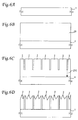
- Figs. 4A-D are structural cross sectional views of each of processes illustrating main parts of the manufacturing processes of a photovoltaic device according to a first embodiment of this invention;
- Fig. 5 is a structural cross sectional view of the photovoltaic device according to the first embodiment;
- Figs. 6A-D are structural cross sectional views of each of processes illustrating main parts of the manufacturing processes of a photovoltaic device according to a second embodiment of this invention
-
- Explanation is made on a manufacturing method of a photovoltaic device according to embodiments of the present invention provided in connection with the above view. Most of processes in this manufacturing method according to the embodiments are the same as the conventional processes, and features of this invention are explained by referring to Figs. 2A-2E explained previously and Figs. 4A-4D for illustrating the features of this invention.
- As shown in Fig. 2A, a
zinc oxide film 21 is formed on asubstrate 1 by sputtering. - Then, a predetermined part of the
zinc oxide film 21 is eliminated by laser beam irradiation and is divided into a plurality of thefirst electrodes 2. At this stage, adiffusion region 1A on thesubstrate 1 and residual 21A of the zinc oxide film seem to be generated, as shown in Figs. 3A-3B. - The surface of the
substrate 1 provided with a plurality of the dividedfirst electrodes 2 is etched. By this etching, the residual 21A of zinc oxide and thediffusion region 1A are eliminated. The etching may be dry etching or wet etching; any of methods capable of eliminating thediffusion region 1A on thesubstrate 1 and the residual 21A of zinc oxide. To eliminate them, selection of etching gas or etching solvent is important. It is required to select etching gas or etching solvent capable of etching component of thesubstrate 1 and zinc oxide. For example, chlorine solvent and acetic acid solvent are preferred for wet etching, but any one capable of etching component of thesubstrate 1 and zinc oxide can be used. - Then, as shown in Fig. 2C, a p-type amorphous silicon carbide film of approximately 100Å, an intrinsic amorphous silicon film of approximately 4000 Å, and an n-type amorphous silicon film of approximately 200Å are laminated in this order on the
substrate 1 so as to cover the etchedfirst electrodes 2 to form anamorphous semiconductor film 31. - As shown in Fig. 2D, a predetermined part of the
amorphous semiconductor film 31 is eliminated by laser beam irradiation and is divided into a plurality of photovoltaic conversion layers 3.
As shown in Fig. 2E, ametal film 41 of silver is formed on thesubstrate 1 so as to cover the photovoltaic conversion layers 3 by sputtering. Then, a predetermined part of themetal film 41 is eliminated by laser beam irradiation and is divided into a plurality of thesecond electrodes 4 to manufacture an integrated photovoltaic device. - By the etching after eliminating the zinc oxide film by laser beam irradiation, the
diffusion region 1A on thesubstrate 1 and the residual 21A of zinc oxide are eliminated. Therefore, leak current between the adjacent first electrodes is greatly reduced as compared with the conventional case, and a photovoltaic device having excellent photovoltaic characteristics is produced in this invention. - Followings are detailed explanation on a first embodiment of this invention by referring to Figs. 4A-4D.
- In the first embodiment, as shown in Fig. 4A, a glass substrate is prepared as the
substrate 1. A size of the substrate is 30 × 40cm and 5mm in thickness. - As shown in Fig. 4B, the
zinc oxide film 21 of approximately 1µ m is formed on an approximately entire surface of thesubstrate 1 by sputtering. Conditions for forming the zinc oxide film is shown in Table 1.Target ZnO (Al2O3 dope : 2 wt.%) Applied RF power 400W Pressure 13.33Pa Sputtering gas Ar : 20SCCM Substrate temperature 170°C - As shown in Fig. 4C, a predetermined part of the
zinc oxide film 21 is eliminated by irradiation of YAG laser beam of wavelength 1.06µ m, pulse frequency 3kHz, and intensity 4.0 × 10⁷ W/cm2, and is divided into a plurality of thefirst electrodes 2. Thezinc oxide film 21 is not completely eliminated by the YAG laser beam irradiation under these conditions, and the residual 21A of the zinc oxide film is found on the surface of thesubstrate 1. - Then, as shown in Fig. 4D, the
substrate 1 having the plurality of thefirst electrodes 2 is immersed in chlorine solution of 0.5 wt.% for about 30 minutes, is etched, and is cleaned with pure water. By this etching, a texture plane is formed on the surface of thefirst electrode 2. - And, as shown in the above mentioned Figs. 2A-2E, a p-type amorphous silicon carbide layer of approximately 100Å, an intrinsic amorphous silicon layer of approximately 1500Å, a n-type microcrystalline silicon layer of approximately 200Å, a p-type amorphous silicone layer of approximately 100Å, an intrinsic amorphous silicon germanium layer of approximately 1000Å, and a n-type amorphous silicon layer of approximately 200Å are laminated in this order by plasma CVD so as to form an
amorphous semiconductor film 31. Formation conditions of each of the layers are shown in Table 2. In this case, reaction pressure is controlled to be 50Pa.Reaction gas Substrate temperature (°C) RF power (W) First p -layer SiH4 : 10SCCM CH4 : 5SCCM 100ppmB2H6 : 5SCCM H2 : 150SCCM 150 200 First i-layer SiH4 : 50SCCM H2 : 100SCCM 200 200 First n-layer SiH4 10SCCM 1%PH3 : 5SCCM H2 : 100SCCM 200 500 Second p-layer SiH4 10SCCM CH4 : 5SCCM 100ppmB2H5 : 5SCCM H2 : 150SCCM 150 200 Second i-layer SiH4 50SCCM GeH4 : 10SCCM H2 : 100SCCM 200 200 Second n-layer SiH4 10SCCM 1%PH3 : 5SCCM H2 : 100SCCM 200 200 - A predetermined part of the
amorphous semiconductor film 31 is eliminated by irradiation of YAG laser beams of wavelength 1.06 µm, pulse frequency 3kHz, and intensity 1.3 × 10⁸W/cm2, and is divided into a plurality of photovoltaic conversion layers 3. - Then, a
metal film 41 of silver of approximately 1µ m is formed on thesubstrate 1 by sputtering so as to cover the photovoltaic conversion layers 3, and a predetermined part of themetal film 41 is eliminated by irradiation of Ar laser beams of wavelength 0.51 µ m andintensity 2 × 10³W/cm2, and is divided into a plurality ofsecond electrodes 4 to produce a photovoltaic device of this embodiment. - A photovoltaic device for comparison is manufactured by the same method as in the case of the first embodiment except for the etching process after division for forming the
first electrodes 2. - Table 3 shows measurement of a resistance value between the adjacent
first electrodes 2 of the photovoltaic device of the embodiment and of the photovoltaic device of the comparison example. Table 4 shows measurement of the photovoltaic characteristics when light of AM1.5, 100mW/cm2 is irradiated to the photovoltaic devices of the embodiment and the comparison example.Insulation resistance (M Ω) Embodiment ∞ Comparison example 600 Ω Voc/stage (V) Isc (mA/cm2) F. F. Efficiency (%) First embodiment 1.5 8.5 0.71 9.1 Comparison example 1.5 8.5 0.67 8.5 - As shown in Table 3, the insulation resistance of the adjacent
first electrodes 2 of the first embodiment improves. In connection with this, as shown in Table 4, F.F. of the embodiment improves and high photovoltaic efficiency is obtained. - As described above, this invention can produce a photovoltaic device having excellent photovoltaic characteristics as compared with the conventional one even when zinc oxide is used for the first electrode.
- Furthermore, the texture plane formed on the surface of the first electrode by the etching process after division for forming the first electrodes scatters incident light, leading to improved photovoltaic characteristics.
- Meantime, energy is required to be applied for momentarily increasing a temperature up to a melting point of approximately 2000°C for processing the transparent electrode by using energy beams. Therefore, when the energy beams are irradiated for dividing the transparent electrode into a plurality of regions, the energy is transmitted to glass. As a result, a temperature increases up to higher than 500°C locally, causing fine cracks and irregular degradation of strength of the glass.
- When the transparent electrode can not be electrically separated completely by scattered attachment generated in separating the transparent electrode by energy beams, a process such as etching or the like is effective for separation. At that time, as shown in Fig. 5, if a
part 21B between thesubstrate 1 and thetransparent electrode 2 which is readily etched is over-etched, thetransparent electrode 2 in proximity of a part to be processed may be peeled, resulting in degraded reliability and characteristics of the device. - A second embodiment provides a method for readily using reinforced glass and preventing over-etching.
- Followings are explanation on the second embodiment of this invention by referring to Figs. 6A-6D.
- As shown in Fig. 6A, a reinforced glass substrate is used as a
substrate 1. The size is 30 × 40cm, 5mm in thickness. And as shown in Fig. 6B, azinc oxide film 21 of 8000Å is formed on an approximately entire surface of thesubstrate 1 by sputtering. Conditions for forming the zinc oxide film are same as shown in Table 1. - As shown in Fig. 6C, a predetermined part of the
zinc oxide film 21 is processed with Nd:YAG laser of 1.06 µm wavelength, 3kHz pulse frequency, 2.0X 10⁶W/cm2 laser power density, and 10mm/sec. processing rate to divide into a plurality of regions so as to form a photovoltaic device of 35-stage integrated connection. The dividing process by the YAG laser intentionally leaves thezinc oxide film 21C in a divided region. In the irradiation of YAG laser under the above conditions, thezinc oxide film 21C of approximately 2000Å is intentionally left after processing. - Then as shown in Fig. 6D, the
substrate 1 processed with laser beams is immersed in chlorine solution of 1.0 wt.% for approximately 20 seconds and is etched to eliminate the remained zinc oxide film, and thesubstrate 1 is cleaned with pure water. A thickness of the zinc oxide film to be etched under the above conditions is approximately 2500Å. The remained zinc oxide film is eliminated and a plurality of thefirst electrodes 2 are formed. By the etching under these conditions, a texture plane on the surface of thefirst electrode 2 is formed. After the etching, a cross section of the first electrode processed with energy beams is observed by a SEM with a magnification rate of 10,000. It was found from the observation that the residual of the zinc oxide film was eliminated from the processed part. Furthermore, when the resistance value between the adjacentfirst electrodes 2 is measured by a tester, the value was more than 1MΩ and it was found that the electrodes were electrically separated. - Then, a p-type amorphous silicon carbide layer of approximately 100Å, an intrinsic amorphous silicon layer of approximately 1500 Å , a n-type microcrystalline silicon layer of approximately 200Å, a p-type amorphous silicon layer of approximately 100Å, an intrinsic amorphous silicon germanium layer of approximately 1000Å, and a n-type amorphous silicon layer of approximately 200 Å are laminated in this order by plasma CVD on the
substrate 1 so as to cover thefirst electrodes 2 to form anamorphous semiconductor film 31. Conditions for forming each of the layers are same as shown in Table 2. - YAG laser secondary harmonic of 0.53 µ m wavelength, 3kHz pulse frequency is irradiated to a predetermined part of the
amorphous semiconductor film 31 with 2X 10⁷W/cm2 laser power density, 10mm/sec. processing rate for obtaining good workability, to divide into a plurality of photovoltaic conversion layers 3. - A
metal film 41 of aluminum of approximately 4000 Å is formed on thesubstrate 1 so as to cover the photovoltaic conversion layers 3 by DC sputtering. This film is formed by applying power of 0.1kW to an A1 target of 300cm2 under an atmosphere of Ar of 400sccm, 1Pa. YAG laser secondary harmonic of 0.53 µ m wavelength, 3kHz pulse frequency is irradiated to a predetermined part of the metal film with 2×10⁷W/cm2 laser power density, 10mm/sec. processing rate for obtaining good workability, to divide into a plurality of second electrodes. By these processes, the photovoltaic device of the second embodiment is produced. - For comparison, the predetermined part of the
zinc oxide film 21 of approximately 8000Å is processed with Nd:YAG laser of 1.06 µm wavelength, 3kHz pulse frequency, 2.0×10⁷W/cm2 laser power density, and 10mm/sec. processing rate to divide into a plurality of regions so as to form a photovoltaic device of 35 stage integrated connection. Then, thesubstrate 1 processed with laser beams is immersed in chlorine solution of 1.0 wt.% for approximately 20 seconds and is etched. The remained zinc oxide film is eliminated, and thesubstrate 1 is cleaned with pure water. And a photovoltaic device of the first embodiment is produced in the same way as in the second embodiment. Light of AM1.5, 100mW/cm2 is irradiated to the photovoltaic devices of the first embodiment and the second embodiment, and the photovoltaic characteristics under 25°C are measured. The results are shown in Table 5.Voc/stage(V) Isc (mA/cm2) F. F. Efficiency(%) First embodiment 1.5 8.5 0.71 9.1 Second embodiment 1.5 8.5 0.73 9.1 - As shown in Table 5, F.F in the second embodiment improves as compared with the first embodiment.
- When observing a cross section of an element by a SEM, peeling of the zinc oxide film at an interface of the glass substrate and the zinc oxide film caused by over-etching is observed after the etching in the first embodiment, and degradation of F.F seems to be caused by increase of leakage component. On the other hand, over-etching is not observed in the second embodiment.
- Table 6 compares an average breaking weight of a blue plate glass and a reinforced glass used in the first and second embodiments, wherein the parameter is 50.
2nd embodiment (reinforced) 1st embodiment (reinforced) 2nd embodiment (blue plate) 1st embodiment (blue plate) Average breaking weight (kgf) 2500 650 900 800 - As indicated in Table 6, strength of the reinforced glass is maintained in the second embodiment. In the first embodiment, on the other hand, when the reinforced glass is used as a substrate, the strength is degraded as compared with the case of the blue plate glass which is not reinforced. Furthermore, it was found that the strength of the blue plate glass of the second embodiment is a little superior to that of the first embodiment.
- This is because heat from irradiation energy transmits to the glass as a base in separating the transparent electrode by laser beams, and the temperature increases up to higher than 500°C locally even when the substrate is the reinforced glass. Thus, the strength is irregularly degraded and the strength as the entire glass substrate is degraded. When observing a cross section of a glass surface of the processed part by a SEM, fine cracks are observed partially in the first embodiment. On the other hand, no crack is observed and mechanical strength is improved in the second embodiment.
- Then, a thickness of the film intentionally remained on the glass substrate of the transparent electrode is changed in the process for dividing into a plurality of regions by energy beams in the second embodiment. That is, in the process for dividing into a plurality of regions by energy beams, a thickness of the film intentionally remained on the transparent electrode is changed by controlling laser power and/or processing rate. Relative comparison is made on output of a solar cell using these substrates. In Table 7, laser power is changed and processing rate is made constant at 10mm/sec. The case of the thickness of remained film 2000Å is used as a reference. The film is etched by chlorine of 1 wt.% for 20 seconds. The thickness of the film to be etched is 2500Å in this case.
Power density Thickness of remained film (Å) Relative output after etched 2 × 10⁷ 0 0.81 1 × 10⁷ 250 0.81 8 × 10⁶ 500 0.97 4 × 10⁶ 1000 1.01 2 × 10⁶ 2000 1.00 1 × 10⁶ 2500 0.87 - As shown in Table 7, when a film is intentionally remained not more than 10% to the thickness to be etched, over-etching is not fully suppressed, resulting in degradation of output. In this experiment, when a film is intentionally remained not less than 20% to the thickness to be etched, output is improved as compared with the first embodiment and the greater output can be obtained as long as the thickness to be remained is not beyond the thickness to be etched.
- When the thickness of a film to be remained is not less than the thickness to be etched, any improvement was not found. Therefore, a thickness to be remained is preferably 20-80% of the thickness to be etched.
- In the process for dividing into a plurality of regions by energy beams in the second embodiment, the transparent electrode of not less than a predetermined thickness is intentionally remained on a side of the glass substrate of the transparent electrode, and the adjacent divided regions are electrically separated in an etching process. These processes solve the problem of fine cracks and irregular degradation of strength, which leads to degradation of strength of the substrate, caused by heat of irradiation energy transmitted to the glass in processing the transparent electrode by energy beams.
- In addition, over-etching of a part easily etched between the substrate and the transparent electrode in a case that attachment of scattered material (its thickness is less than a few dozens Å) generated in processing the transparent electrode by energy beams is prevented and reliability and characteristics of the device can be improved by preventing peeling of a transparent conductive film in proximity of the processed part.
- The second embodiment is further effective in using a reinforced glass. When a temperature of the reinforced glass increases to about 500°C, nearly at a glass fusing temperature, the reinforced glass is not effective. Therefore, the insulating film and the transparent conductive film are formed under a temperature not higher than 500°C. As compared with tin oxide, relatively good light transmittivity and conductivity can be obtained at not higher than 500°C particularly in using zinc oxide.
- In this embodiment, zinc oxide formed by DC sputtering is used as the transparent electrode. This is because good film characteristics can be obtained at a relatively low substrate temperature 300 °C . If sufficient conductive characteristics can be obtained at a temperature not higher than around 500°C, other material such as tin oxide and other method of formation such as MOCVD are applicable.
- Although this embodiment does not form coating of insulating inorganic material on a surface of the glass substrate, the same effect can be obtained in a case of a glass substrate coated with the insulating inorganic material.
- Although this embodiment describes on an example of application to the integrated solar cell device of this invention, this invention can be applied to a pin single layer solar cell device.
- Although application to a photovoltaic device having component of amorphous silicon, amorphous carbonized silicon, and microcrystalline silicon is described in this embodiment, a semiconductor element of other structure using a thin film semiconductor containing other component can obtain the same effect.
- This invention can be applied not only to a solar cell but to a photovoltaic device such as a photo sensor or the like.
- In the above embodiment, although YAG laser beams are used as energy beams for separating the transparent electrode, line beams of excimer laser can be used for separation.
- Although the present invention has been described and illustrated in detail, it is clearly understood that the same is and example only and is not to be taken by way of limitation by way of illustration, the spirit and scope of the present invention being limited only by the terms of the appended claims.
Claims (10)
- A manufacturing method of a photovoltaic device provided with a plurality of unit cells including a first electrode of zinc oxide, a photovoltaic conversion layer, and a second electrode on a surface of a transparent substrate, comprisinga process for forming a zinc oxide film on a surface of a substrate,a process for eliminating a predetermined part of the zinc oxide film by energy beam irradiation and dividing the zinc oxide film into a plurality of the first electrodes, anda process for etching the surface of the substrate provided with the plurality of the first electrodes.
- The manufacturing method of a photovoltaic device according to claim 1, wherein
a texture plane is formed on a surface of the first electrode by etching. - The manufacturing method of a photovoltaic device according to claim 1, wherein
the etching is provided by wet-etching using acid or dry-etching using halogen gas. - The manufacturing method of a photovoltaic device according to claim 1, wherein
the energy beam is a solid laser beam of YAG laser or a line beam of an excimer laser. - A manufacturing method of a photovoltaic device provided with a plurality of unit cells including a first electrode of zinc oxide, a photovoltaic conversion layer, and a second electrode on a surface of a transparent substrate, comprisinga process for forming a zinc oxide film on a surface of a substrate,a process for eliminating a predetermined part of the zinc oxide film by energy beam irradiation so as to leave the zinc oxide film of not less than a predetermined thickness on a side of the transparent substrate and preliminarily dividing the zinc oxide film into a plurality of the first electrodes, anda process for etching the surface of the substrate provided with the plurality of the first electrodes which are preliminarily divided, and electrically separating adjacent divided areas.
- The manufacturing method of a photovoltaic device according to claim 5, wherein
the transparent substrate is a reinforced glass. - The manufacturing method of a photovoltaic device according to claim 5, wherein
the thickness of the film remained on the side of the transparent substrate is 20-80 % of a thickness of the film to be eliminated by etching. - The manufacturing method of a photovoltaic device according to claim 5, wherein
a texture plane is formed on a surface of the first electrode by etching. - The manufacturing method of a photovoltaic device according to claim 5, wherein
the etching is provided by wet-etching using acid or dry-etching using halogen gas. - The manufacturing method of a photovoltaic device according to claim 5, wherein
the energy beam is a solid laser beam of YAG laser or a line beam of an excimer laser.
Applications Claiming Priority (2)
| Application Number | Priority Date | Filing Date | Title |
|---|---|---|---|
| JP33698599 | 1999-11-29 | ||
| JP33698599 | 1999-11-29 |
Publications (2)
| Publication Number | Publication Date |
|---|---|
| EP1104030A2 true EP1104030A2 (en) | 2001-05-30 |
| EP1104030A3 EP1104030A3 (en) | 2001-09-05 |
Family
ID=18304424
Family Applications (1)
| Application Number | Title | Priority Date | Filing Date |
|---|---|---|---|
| EP00126006A Withdrawn EP1104030A3 (en) | 1999-11-29 | 2000-11-28 | Manufacturing method of photovoltaic device |
Country Status (2)
| Country | Link |
|---|---|
| US (1) | US6348362B1 (en) |
| EP (1) | EP1104030A3 (en) |
Cited By (8)
| Publication number | Priority date | Publication date | Assignee | Title |
|---|---|---|---|---|
| DE102004017680A1 (en) * | 2004-04-10 | 2005-10-27 | Forschungszentrum Jülich GmbH | Method for cleaning and etching a substrate with a transparent, conductive oxide layer, and device for carrying out the method |
| DE102008051730A1 (en) | 2008-10-15 | 2010-04-22 | Saint-Gobain Sekurit Deutschland Gmbh & Co. Kg | Transparent article having a localized, structured, electrically heatable, transparent region, process for its preparation and its use |
| CN101496178B (en) * | 2006-07-31 | 2010-11-10 | 三洋电机株式会社 | Solar cell module |
| EP2256856A1 (en) | 2009-05-28 | 2010-12-01 | Saint-Gobain Glass France | Transparent, flat device for receiving and/or transmitting electromagnetic radiation with at least one other function, method for producing same and use of same |
| DE102009025888A1 (en) | 2009-05-29 | 2010-12-02 | Saint-Gobain Sekurit Deutschland Gmbh & Co. Kg | Electrically extensively heatable, transparent object, process for its preparation and its use |
| DE202010017313U1 (en) | 2010-05-20 | 2011-10-27 | Saint-Gobain Glass France | Transparent, sheet-like device for receiving and / or transmitting electromagnetic radiation with at least one further function |
| US8872703B2 (en) | 2009-01-16 | 2014-10-28 | Saint-Gobain Glass France | Transparent, flat antenna, suitable for transmitting and receiving electromagnetic waves, method for the production thereof, and use thereof |
| TWI460853B (en) * | 2011-06-10 | 2014-11-11 | Mitsubishi Materials Corp | A transparent conductive film for organic EL and an organic EL element using the transparent conductive film |
Families Citing this family (1)
| Publication number | Priority date | Publication date | Assignee | Title |
|---|---|---|---|---|
| KR101476120B1 (en) * | 2008-06-12 | 2014-12-26 | 주성엔지니어링(주) | Thin film type Solar Cell and Method for manufacturing the same |
Citations (5)
| Publication number | Priority date | Publication date | Assignee | Title |
|---|---|---|---|---|
| EP0322258A2 (en) * | 1987-12-23 | 1989-06-28 | Semiconductor Energy Laboratory Co., Ltd. | Method for producing thin film patterns on substrates |
| EP0324550A1 (en) * | 1988-01-06 | 1989-07-19 | Semiconductor Energy Laboratory Co., Ltd. | Thin film pattern structure |
| EP0554877A1 (en) * | 1992-02-05 | 1993-08-11 | Canon Kabushiki Kaisha | Photovoltaic device and method for producing the same |
| EP0827212A2 (en) * | 1996-08-26 | 1998-03-04 | Sharp Kabushiki Kaisha | Method of fabricating integrated thin film solar cells |
| US5976396A (en) * | 1998-02-10 | 1999-11-02 | Feldman Technology Corporation | Method for etching |
Family Cites Families (4)
| Publication number | Priority date | Publication date | Assignee | Title |
|---|---|---|---|---|
| US4772335A (en) * | 1987-10-15 | 1988-09-20 | Stemcor Corporation | Photovoltaic device responsive to ultraviolet radiation |
| JP2983684B2 (en) * | 1991-05-23 | 1999-11-29 | 三洋電機株式会社 | Method for manufacturing photovoltaic device |
| US5800632A (en) * | 1995-09-28 | 1998-09-01 | Canon Kabushiki Kaisha | Photovoltaic device and method for manufacturing it |
| CA2267076C (en) * | 1996-09-26 | 2005-01-25 | Akzo Nobel Nv | Method of manufacturing a photovoltaic foil |
-
2000
- 2000-11-28 EP EP00126006A patent/EP1104030A3/en not_active Withdrawn
- 2000-11-28 US US09/722,718 patent/US6348362B1/en not_active Expired - Lifetime
Patent Citations (5)
| Publication number | Priority date | Publication date | Assignee | Title |
|---|---|---|---|---|
| EP0322258A2 (en) * | 1987-12-23 | 1989-06-28 | Semiconductor Energy Laboratory Co., Ltd. | Method for producing thin film patterns on substrates |
| EP0324550A1 (en) * | 1988-01-06 | 1989-07-19 | Semiconductor Energy Laboratory Co., Ltd. | Thin film pattern structure |
| EP0554877A1 (en) * | 1992-02-05 | 1993-08-11 | Canon Kabushiki Kaisha | Photovoltaic device and method for producing the same |
| EP0827212A2 (en) * | 1996-08-26 | 1998-03-04 | Sharp Kabushiki Kaisha | Method of fabricating integrated thin film solar cells |
| US5976396A (en) * | 1998-02-10 | 1999-11-02 | Feldman Technology Corporation | Method for etching |
Cited By (10)
| Publication number | Priority date | Publication date | Assignee | Title |
|---|---|---|---|---|
| DE102004017680A1 (en) * | 2004-04-10 | 2005-10-27 | Forschungszentrum Jülich GmbH | Method for cleaning and etching a substrate with a transparent, conductive oxide layer, and device for carrying out the method |
| DE102004017680B4 (en) * | 2004-04-10 | 2008-01-24 | Forschungszentrum Jülich GmbH | Process for the treatment of substrates with prestructured zinc oxide layers |
| CN101496178B (en) * | 2006-07-31 | 2010-11-10 | 三洋电机株式会社 | Solar cell module |
| DE102008051730A1 (en) | 2008-10-15 | 2010-04-22 | Saint-Gobain Sekurit Deutschland Gmbh & Co. Kg | Transparent article having a localized, structured, electrically heatable, transparent region, process for its preparation and its use |
| US8872703B2 (en) | 2009-01-16 | 2014-10-28 | Saint-Gobain Glass France | Transparent, flat antenna, suitable for transmitting and receiving electromagnetic waves, method for the production thereof, and use thereof |
| EP2256856A1 (en) | 2009-05-28 | 2010-12-01 | Saint-Gobain Glass France | Transparent, flat device for receiving and/or transmitting electromagnetic radiation with at least one other function, method for producing same and use of same |
| DE102009025888A1 (en) | 2009-05-29 | 2010-12-02 | Saint-Gobain Sekurit Deutschland Gmbh & Co. Kg | Electrically extensively heatable, transparent object, process for its preparation and its use |
| US9277597B2 (en) | 2009-05-29 | 2016-03-01 | Saint-Gobain Glass France | Electrically extensively heatable, transparent object, method for the production thereof, and use thereof |
| DE202010017313U1 (en) | 2010-05-20 | 2011-10-27 | Saint-Gobain Glass France | Transparent, sheet-like device for receiving and / or transmitting electromagnetic radiation with at least one further function |
| TWI460853B (en) * | 2011-06-10 | 2014-11-11 | Mitsubishi Materials Corp | A transparent conductive film for organic EL and an organic EL element using the transparent conductive film |
Also Published As
| Publication number | Publication date |
|---|---|
| US6348362B1 (en) | 2002-02-19 |
| EP1104030A3 (en) | 2001-09-05 |
Similar Documents
| Publication | Publication Date | Title |
|---|---|---|
| US7964431B2 (en) | Method to make electrical contact to a bonded face of a photovoltaic cell | |
| EP1727211B1 (en) | Method of fabricating a thin-film solar cell, and thin-film solar cell | |
| US8945976B2 (en) | Method for making solar cell having crystalline silicon P—N homojunction and amorphous silicon heterojunctions for surface passivation | |
| JP4194468B2 (en) | Solar cell and method for manufacturing the same | |
| WO2012020682A1 (en) | Crystalline silicon solar cell | |
| US20010035205A1 (en) | Integrated thin-film solar battery and method of manufacturing the same | |
| JP2004014958A (en) | Thin film polycrystalline solar cell and manufacturing method therefor | |
| KR20070119702A (en) | Solar cell | |
| JP2003273383A (en) | Solar cell element and manufacturing method therefor | |
| KR20080002657A (en) | Photovoltaic device which includes all-back-contact configuration and related processes | |
| CA2906462A1 (en) | Solar cell having crystalline silicon p-n homojunction and amorphous silicon heterojunctions for surface passivation | |
| JP2003347571A (en) | Photovoltaic element and photovoltaic device | |
| JP2002025350A (en) | Substrate with transparent conductive film and manufacturing method of the same, etching method using the same, and light electromotive force device | |
| JP3653800B2 (en) | Method for manufacturing integrated thin film solar cell | |
| JP4171162B2 (en) | Photovoltaic element and manufacturing method thereof | |
| US6348362B1 (en) | Manufacturing method of photovoltaic device | |
| US20100139755A1 (en) | Front connected photovoltaic assembly and associated methods | |
| JP5022341B2 (en) | Photoelectric conversion device | |
| WO2010050035A1 (en) | Process for producing photoelectric conversion apparatus | |
| JP2003282458A (en) | Semiconductor device and method of manufacturing the same | |
| US20100224238A1 (en) | Photovoltaic cell comprising an mis-type tunnel diode | |
| JP4171166B2 (en) | Photovoltaic device and manufacturing method thereof | |
| JPH1084125A (en) | Photoelectric converter and manufacture thereof | |
| JP3243229B2 (en) | Solar cell module | |
| JP4162373B2 (en) | Photovoltaic device manufacturing method |
Legal Events
| Date | Code | Title | Description |
|---|---|---|---|
| PUAI | Public reference made under article 153(3) epc to a published international application that has entered the european phase |
Free format text: ORIGINAL CODE: 0009012 |
|
| AK | Designated contracting states |
Kind code of ref document: A2 Designated state(s): AT BE CH CY DE DK ES FI FR GB GR IE IT LI LU MC NL PT SE TR |
|
| AX | Request for extension of the european patent |
Free format text: AL;LT;LV;MK;RO;SI |
|
| PUAL | Search report despatched |
Free format text: ORIGINAL CODE: 0009013 |
|
| AK | Designated contracting states |
Kind code of ref document: A3 Designated state(s): AT BE CH CY DE DK ES FI FR GB GR IE IT LI LU MC NL PT SE TR |
|
| AX | Request for extension of the european patent |
Free format text: AL;LT;LV;MK;RO;SI |
|
| RIC1 | Information provided on ipc code assigned before grant |
Free format text: 7H 01L 31/18 A, 7H 01L 31/0224 B, 7H 01L 27/142 B |
|
| 17P | Request for examination filed |
Effective date: 20011113 |
|
| AKX | Designation fees paid |
Free format text: DE FR GB |
|
| 17Q | First examination report despatched |
Effective date: 20081219 |
|
| STAA | Information on the status of an ep patent application or granted ep patent |
Free format text: STATUS: THE APPLICATION HAS BEEN WITHDRAWN |
|
| 18W | Application withdrawn |
Effective date: 20120503 |