BACKGROUND OF THE INVENTION
Field of the Invention
This invention relates to an integrated photovoltaic device, particularly relates
to a manufacturing method of a photovoltaic device provided with a transparent
electrode of zinc oxide.
Description of Prior Art
A photovoltaic device such as a solar cell can directly convert sunlight into
electricity and has been commercialized as a new energy source. Such the
photovoltaic device has been formed of crystalline semiconductor material such
as single crystalline silicon and polycrystalline silicon, compound
semiconductor material such as GaAs, InP or the like, and amorphous
semiconductor material such as amorphous silicon and amorphous silicon
germanium or the like. The photovoltaic device using the amorphous
semiconductor material is manufactured at a low temperature as compared
with other semiconductor material, can increase a size easily, and can easily be
integrated on a substrate.
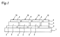
Fig. 1 is a structural cross sectional view of an integrated photovoltaic device
using the amorphous semiconductor material.
Explanation is made on the integrated photovoltaic device by referring to Fig. 1.
A substrate 1 is formed of translucent and insulating material such as glass,
plastic, or the like. A plurality of first electrodes 2 are arranged on a surface of
the substrate 1. The first electrode 2 is formed of tin oxide (SnO2) and has a
rough plane for scattering light incident from the substrate 1 on the surface.
This rough plane is generally referred as a texture plane.
A photovoltaic conversion layer 3 is formed of amorphous semiconductor
material, and generally includes a p-type amorphous silicon carbide film of
approximately 100Å, an intrinsic amorphous silicon film of approximately 4000
A, and an n-type amorphous silicon film of approximately 200Å laminated in
this order from a side of the first electrode 2. A second electrode 4 is formed of a
highly reflective metal film such as Ag, Al or the like.
A lamination body of the first electrode 2, the photovoltaic conversion layer 3,
and the second electrode 4 is a unit cell 10, and adjacent unit cells 10 are
electrically connected in series by electrically linking the first electrode 2 of the
one unit cell 10 and the second electrode 4 of the other unit cell 10.
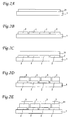
Figs. 2A-2E are structural cross sectional views of each of processes for
illustrating manufacturing processes of the conventional photovoltaic device.
As shown in Fig. 2A, a transparent electrode film 21 of tin oxide (SnO2) having a
texture plane is formed on a surface of the substrate 1. A predetermined part of
the transparent electrode film 21 is eliminated by laser beam irradiation and is
divided into a plurality of the first electrodes 2, as shown in Fig. 2B.
An amorphous semiconductor film 31 having pin junction inside is formed on
the substrate so as to cover over the first electrodes 2 as shown in Fig. 2C.
Then, a predetermined part of the amorphous semiconductor film 31 is
eliminated by laser beam irradiation and is divided into a plurality of the
photovoltaic conversion layers 3 as shown in Fig. 2D.
A metal film 4 is formed on the substrate 1 so as to cover the photovoltaic
conversion layers 3 as shown in Fig. 2E. Then, a predetermined part of the metal
film 41 is eliminated by laser beam irradiation and is divided into a plurality of
the second electrodes 4 to produce the photovoltaic device as shown in Fig. 1.
The material for forming the first electrode as the transparent electrode is
conventionally SnO2. However, formation of SnO2 requires a temperature higher
than approximately 500°C, resulting in an increase in manufacture cost. And a
substrate of less heat resistance such as plastic can not be usable and selection
of substrate material is limited.
In conjunction with this, zinc oxide as material for the first electrode has been
considered. The first electrode of zinc oxide can be prepared at a low
temperature of not higher than 200°C by sputtering, resulting in reduction of
manufacture cost. In addition, selection of the substrate material is not limited
as tightly as in the conventional case.
SUMMARY OF THE INVENTION
The applicants of this invention have examined and found that it is more
difficult to electrically separate the adjacent first electrodes of zinc oxide in
eliminating the predetermined part of the zinc oxide film by laser beam
irradiation and dividing into a plurality of the first electrodes as compared with
the first electrode of a SnO2 film. Thus, leak current is likely to occur between
adjacent unit cells of the photovoltaic device comprising the first electrodes of
zinc oxide and the photovoltaic conversion characteristics are degraded.
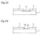
A cause of the above problem has been examined. An expected cause of the
problem is explained by referring to schematic cross sectional views of Figs.
3A-3B. Elements having the same functions as in Fig. 1 have the same reference
numerals.
When laser beam intensity for irradiating to the zinc oxide film is great, the
temperature of the zinc oxide film increases and doping material of Al, Mg, Ga or
the like for reducing a resistance value included in the zinc oxide film is
scattered in the substrate 1 to form the diffusion region 1A on a surface of the
substrate as shown in Fig. 3A. And leak current is generated between the
adjacent first electrodes 2, 2 through the diffusion region 1A.
On the other hand, when laser beam intensity is small so as to suppress
formation of the diffusion region 1A, the residual 21A of the zinc oxide film 21 is
generated as shown in Fig. 3B and leak current occurs between the adjacent
first electrodes 2 through the residual 21A.
When the first electrode is formed of zinc oxide and intensity of laser beams to
be irradiated is great, doping material of Al, Mg, Ga or the like included in the
zinc oxide is scattered and the diffusion region is formed on a surface of the
substrate. When the intensity of the laser beams is small, residual of zinc oxide
is generated. In these cases, it is expected that leak current occurs between the
adjacent first electrodes through the diffusion region and the residual, and
photovoltaic conversion characteristic are degraded.
In recent years, a thin film semiconductor device using a glass substrate has
become large. A solar cell device which is used in the outside is particularly
required to have mechanical strength. In conjunction with this, only attachment
of a reinforced glass which requires complicated processes and is difficult to
reduce production cost, and a reinforcement process, as a post-process, of a
glass substrate with a transparent electrode which is difficult to have sufficient
strength and film characteristics have been considered. In this case, when a
temperature of the reinforced glass increases higher than 500°C of a glass
melting point after the reinforcement process, an effect of reinforcement and, as
a result, the strength may be degraded. Although a SnO2 film is commonly used
material, this film can have sufficient characteristics only when formed at
higher than 500°C. Therefore, the reinforced glass can not be used as a
substrate. Thus, a method for reinforcing a glass substrate after mounting a
transparent electrode has been examined.
In processing the transparent electrode by energy beams, the energy beams
should be applied so that the temperature increases momentarily up to
approximately 2000°C of a melting point. Therefore, heat from irradiation
energy transmits to a side of the glass when the energy beams are irradiated in
order to divide the transparent electrode into a plurality of regions even though
the transparent electrode of good characteristics are formed at lower than 500°C.
As a result, the temperature increases up to higher than 500°C locally, which
causes fine cracks and irregular degradation of strength of the part of the glass
to degrade the strength of the entire glass.
This invention was made to solve the existing problem and provides a
manufacturing method of a photovoltaic device comprising a first electrode of
zinc oxide capable of improving photovoltaic conversion characteristics.
This invention provides a manufacturing method capable of using reinforced
glass as a substrate, improving photovoltaic conversion characteristic, and
having sufficient mechanical strength
A manufacturing method of a photovoltaic device provided with a plurality of
unit cells including a first electrode of zinc oxide, a photovoltaic conversion layer,
and a second electrode on a surface of a transparent substrate, comprises a
process for forming a zinc oxide film on a surface of a substrate, a process for
eliminating a predetermined part of the zinc oxide film by energy beam
irradiation and dividing the zinc oxide film into a plurality of the first electrodes,
and a process for etching the surface of the substrate provided with the plurality
of the first electrodes.
A texture plane is formed on a surface of the first electrode by etching.
In this invention, a predetermined part of the zinc oxide film is eliminated by
energy beam irradiation and the zinc oxide film is divided into a plurality of the
first electrodes. Then, a diffusion region and residual of zinc oxide formed on a
surface of the substrate are eliminated by etching. Leak current between the
adjacent first electrodes decreases greatly as compared with the conventional
case. Therefore, a photovoltaic device with excellent photovoltaic conversion
characteristics can be provided by this invention.
A manufacturing method of a photovoltaic device provided with a plurality of
unit cells including a first electrode of zinc oxide, a photovoltaic conversion layer,
and a second electrode on a surface of a transparent substrate, comprising a
process for forming a zinc oxide film on a surface of a substrate, a process for
eliminating a predetermined part of the zinc oxide film by energy beam
irradiation so as to leave the zinc oxide film of not less than a predetermined
thickness on a side of the transparent substrate and preliminarily dividing the
zinc oxide film into a plurality of the first electrodes, and a process for etching
the surface of the substrate provided with the plurality of the first electrodes
which are preliminarily divided, and electrically separating adjacent divided
areas.
The transparent substrate is a reinforced glass.
In this invention, the transparent electrode of more than a predetermined
thickness is intentionally remained on a glass substrate side of the transparent
electrode in a process for dividing into a plurality of regions by energy beams,
and the adjacent divided regions are electrically separated in the etching
process. Degradation of substrate strength caused by fine cracks and irregular
degradation of strength caused by heat transmitted to the glass in processing
the transparent electrodes by energy beams is prevented with these processes.
In addition, development of over-etching is prevented in a readily etched part
between the substrate and the transparent electrodes when attachment of
scattered material generated in processing the transparent electrodes by energy
beam prevents complete separation of the transparent electrodes. Thus, peeling
of a transparent conductive film in proximity of a processed part is prevented
and reliability and performance of a device are improved.
The above second constitution prevents an increase of a temperature to a
melting point of glass and maintains an effect of reinforcement, thus is
particularly effective in using reinforced glass.
BRIEF DESCRIPTION OF THE TRAWINGS
DESCRIPITION OF PREFERRED EMBODIMENTS
Explanation is made on a manufacturing method of a photovoltaic device
according to embodiments of the present invention provided in connection with
the above view. Most of processes in this manufacturing method according to
the embodiments are the same as the conventional processes, and features of
this invention are explained by referring to Figs. 2A-2E explained previously and
Figs. 4A-4D for illustrating the features of this invention.
As shown in Fig. 2A, a zinc oxide film 21 is formed on a substrate 1 by
sputtering.
Then, a predetermined part of the zinc oxide film 21 is eliminated by laser beam
irradiation and is divided into a plurality of the first electrodes 2. At this stage, a
diffusion region 1A on the substrate 1 and residual 21A of the zinc oxide film
seem to be generated, as shown in Figs. 3A-3B.
The surface of the substrate 1 provided with a plurality of the divided first
electrodes 2 is etched. By this etching, the residual 21A of zinc oxide and the
diffusion region 1A are eliminated. The etching may be dry etching or wet
etching; any of methods capable of eliminating the diffusion region 1A on the
substrate 1 and the residual 21A of zinc oxide. To eliminate them, selection of
etching gas or etching solvent is important. It is required to select etching gas or
etching solvent capable of etching component of the substrate 1 and zinc oxide.
For example, chlorine solvent and acetic acid solvent are preferred for wet
etching, but any one capable of etching component of the substrate 1 and zinc
oxide can be used.
Then, as shown in Fig. 2C, a p-type amorphous silicon carbide film of
approximately 100Å, an intrinsic amorphous silicon film of approximately 4000
Å, and an n-type amorphous silicon film of approximately 200Å are laminated
in this order on the substrate 1 so as to cover the etched first electrodes 2 to
form an amorphous semiconductor film 31.
As shown in Fig. 2D, a predetermined part of the amorphous semiconductor
film 31 is eliminated by laser beam irradiation and is divided into a plurality of
photovoltaic conversion layers 3.
As shown in Fig. 2E, a metal film 41 of silver is formed on the substrate 1 so as
to cover the photovoltaic conversion layers 3 by sputtering. Then, a
predetermined part of the metal film 41 is eliminated by laser beam irradiation
and is divided into a plurality of the second electrodes 4 to manufacture an
integrated photovoltaic device.
By the etching after eliminating the zinc oxide film by laser beam irradiation, the
diffusion region 1A on the substrate 1 and the residual 21A of zinc oxide are
eliminated. Therefore, leak current between the adjacent first electrodes is
greatly reduced as compared with the conventional case, and a photovoltaic
device having excellent photovoltaic characteristics is produced in this
invention.
Followings are detailed explanation on a first embodiment of this invention by
referring to Figs. 4A-4D.
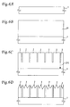
In the first embodiment, as shown in Fig. 4A, a glass substrate is prepared as
the substrate 1. A size of the substrate is 30 × 40cm and 5mm in thickness.
As shown in Fig. 4B, the
zinc oxide film 21 of approximately 1µ m is formed on
an approximately entire surface of the
substrate 1 by sputtering. Conditions for
forming the zinc oxide film is shown in Table 1.
| Target | ZnO (Al2O3 dope : 2 wt.%) |
| Applied RF power | 400W |
| Pressure | 13.33Pa |
| Sputtering gas | Ar : 20SCCM |
| Substrate temperature | 170°C |
As shown in Fig. 4C, a predetermined part of the zinc oxide film 21 is eliminated
by irradiation of YAG laser beam of wavelength 1.06µ m, pulse frequency 3kHz,
and intensity 4.0 × 10⁷ W/cm2, and is divided into a plurality of the first
electrodes 2. The zinc oxide film 21 is not completely eliminated by the YAG
laser beam irradiation under these conditions, and the residual 21A of the zinc
oxide film is found on the surface of the substrate 1.
Then, as shown in Fig. 4D, the substrate 1 having the plurality of the first
electrodes 2 is immersed in chlorine solution of 0.5 wt.% for about 30 minutes,
is etched, and is cleaned with pure water. By this etching, a texture plane is
formed on the surface of the first electrode 2.
And, as shown in the above mentioned Figs. 2A-2E, a p-type amorphous silicon
carbide layer of approximately 100Å, an intrinsic amorphous silicon layer of
approximately 1500Å, a n-type microcrystalline silicon layer of approximately
200Å, a p-type amorphous silicone layer of approximately 100Å, an intrinsic
amorphous silicon germanium layer of approximately 1000Å, and a n-type
amorphous silicon layer of approximately 200Å are laminated in this order by
plasma CVD so as to form an
amorphous semiconductor film 31. Formation
conditions of each of the layers are shown in Table 2. In this case, reaction
pressure is controlled to be 50Pa.
| | Reaction gas | Substrate temperature (°C) | RF power (W) |
| First p -layer | SiH4 : 10SCCM CH4 : 5SCCM 100ppmB2H6 : 5SCCM H2 : 150SCCM | 150 | 200 |
| First i-layer | SiH4 : 50SCCM H2 : 100SCCM | 200 | 200 |
| First n-layer | SiH4 10SCCM 1%PH3 : 5SCCM H2 : 100SCCM | 200 | 500 |
| Second p-layer | SiH4 10SCCM CH4 : 5SCCM 100ppmB2H5 : 5SCCM H2 : 150SCCM | 150 | 200 |
| Second i-layer | SiH4 50SCCM GeH4 : 10SCCM H2 : 100SCCM | 200 | 200 |
| Second n-layer | SiH4 10SCCM 1%PH3 : 5SCCM H2 : 100SCCM | 200 | 200 |
A predetermined part of the amorphous semiconductor film 31 is eliminated by
irradiation of YAG laser beams of wavelength 1.06 µm, pulse frequency 3kHz,
and intensity 1.3 × 10⁸W/cm2, and is divided into a plurality of photovoltaic
conversion layers 3.
Then, a metal film 41 of silver of approximately 1µ m is formed on the substrate
1 by sputtering so as to cover the photovoltaic conversion layers 3, and a
predetermined part of the metal film 41 is eliminated by irradiation of Ar laser
beams of wavelength 0.51 µ m and intensity 2 × 10³W/cm2, and is divided into a
plurality of second electrodes 4 to produce a photovoltaic device of this
embodiment.
A photovoltaic device for comparison is manufactured by the same method as in
the case of the first embodiment except for the etching process after division for
forming the first electrodes 2.
Table 3 shows measurement of a resistance value between the adjacent
first
electrodes 2 of the photovoltaic device of the embodiment and of the photovoltaic
device of the comparison example. Table 4 shows measurement of the
photovoltaic characteristics when light of AM1.5, 100mW/cm
2 is irradiated to
the photovoltaic devices of the embodiment and the comparison example.
| | Insulation resistance (M Ω) |
| Embodiment | ∞ |
| Comparison example | 600 Ω |
| | Voc/stage (V) | Isc (mA/cm2) | F. F. | Efficiency (%) |
| First embodiment | 1.5 | 8.5 | 0.71 | 9.1 |
| Comparison example | 1.5 | 8.5 | 0.67 | 8.5 |
As shown in Table 3, the insulation resistance of the adjacent first electrodes 2
of the first embodiment improves. In connection with this, as shown in Table 4,
F.F. of the embodiment improves and high photovoltaic efficiency is obtained.
As described above, this invention can produce a photovoltaic device having
excellent photovoltaic characteristics as compared with the conventional one
even when zinc oxide is used for the first electrode.
Furthermore, the texture plane formed on the surface of the first electrode by
the etching process after division for forming the first electrodes scatters
incident light, leading to improved photovoltaic characteristics.
Meantime, energy is required to be applied for momentarily increasing a
temperature up to a melting point of approximately 2000°C for processing the
transparent electrode by using energy beams. Therefore, when the energy
beams are irradiated for dividing the transparent electrode into a plurality of
regions, the energy is transmitted to glass. As a result, a temperature increases
up to higher than 500°C locally, causing fine cracks and irregular degradation
of strength of the glass.
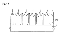
When the transparent electrode can not be electrically separated completely by
scattered attachment generated in separating the transparent electrode by
energy beams, a process such as etching or the like is effective for separation. At
that time, as shown in Fig. 5, if a part 21B between the substrate 1 and the
transparent electrode 2 which is readily etched is over-etched, the transparent
electrode 2 in proximity of a part to be processed may be peeled, resulting in
degraded reliability and characteristics of the device.
A second embodiment provides a method for readily using reinforced glass and
preventing over-etching.
Followings are explanation on the second embodiment of this invention by
referring to Figs. 6A-6D.
As shown in Fig. 6A, a reinforced glass substrate is used as a substrate 1. The
size is 30 × 40cm, 5mm in thickness. And as shown in Fig. 6B, a zinc oxide film
21 of 8000Å is formed on an approximately entire surface of the substrate 1 by
sputtering. Conditions for forming the zinc oxide film are same as shown in
Table 1.
As shown in Fig. 6C, a predetermined part of the zinc oxide film 21 is processed with
Nd:YAG laser of 1.06 µm wavelength, 3kHz pulse frequency, 2.0X 10⁶W/cm2
laser power density, and 10mm/sec. processing rate to divide into a plurality of
regions so as to form a photovoltaic device of 35-stage integrated connection.
The dividing process by the YAG laser intentionally leaves the zinc oxide film
21C in a divided region. In the irradiation of YAG laser under the above
conditions, the zinc oxide film 21C of approximately 2000Å is intentionally left
after processing.
Then as shown in Fig. 6D, the substrate 1 processed with laser beams is
immersed in chlorine solution of 1.0 wt.% for approximately 20 seconds and is
etched to eliminate the remained zinc oxide film, and the substrate 1 is cleaned
with pure water. A thickness of the zinc oxide film to be etched under the above
conditions is approximately 2500Å. The remained zinc oxide film is eliminated
and a plurality of the first electrodes 2 are formed. By the etching under these
conditions, a texture plane on the surface of the first electrode 2 is formed. After
the etching, a cross section of the first electrode processed with energy beams is
observed by a SEM with a magnification rate of 10,000. It was found from the
observation that the residual of the zinc oxide film was eliminated from the
processed part. Furthermore, when the resistance value between the adjacent
first electrodes 2 is measured by a tester, the value was more than 1MΩ and it
was found that the electrodes were electrically separated.
Then, a p-type amorphous silicon carbide layer of approximately 100Å, an
intrinsic amorphous silicon layer of approximately 1500 Å , a n-type
microcrystalline silicon layer of approximately 200Å, a p-type amorphous
silicon layer of approximately 100Å, an intrinsic amorphous silicon germanium
layer of approximately 1000Å, and a n-type amorphous silicon layer of
approximately 200 Å are laminated in this order by plasma CVD on the
substrate 1 so as to cover the first electrodes 2 to form an amorphous
semiconductor film 31. Conditions for forming each of the layers are same as
shown in Table 2.
YAG laser secondary harmonic of 0.53 µ m wavelength, 3kHz pulse frequency is
irradiated to a predetermined part of the amorphous semiconductor film 31 with
2X 10⁷W/cm2 laser power density, 10mm/sec. processing rate for obtaining
good workability, to divide into a plurality of photovoltaic conversion layers 3.
A metal film 41 of aluminum of approximately 4000 Å is formed on the
substrate 1 so as to cover the photovoltaic conversion layers 3 by DC sputtering.
This film is formed by applying power of 0.1kW to an A1 target of 300cm2 under
an atmosphere of Ar of 400sccm, 1Pa. YAG laser secondary harmonic of 0.53 µ
m wavelength, 3kHz pulse frequency is irradiated to a predetermined part of the
metal film with 2×10⁷W/cm2 laser power density, 10mm/sec. processing rate
for obtaining good workability, to divide into a plurality of second electrodes. By
these processes, the photovoltaic device of the second embodiment is produced.
For comparison, the predetermined part of the
zinc oxide film 21 of approximately
8000Å is processed with Nd:YAG laser of 1.06 µm wavelength, 3kHz pulse
frequency, 2.0×10
7W/cm
2 laser power density, and 10mm/sec. processing rate
to divide into a plurality of regions so as to form a photovoltaic device of 35 stage
integrated connection. Then, the
substrate 1 processed with laser beams is
immersed in chlorine solution of 1.0 wt.% for approximately 20 seconds and is
etched. The remained zinc oxide film is eliminated, and the
substrate 1 is
cleaned with pure water. And a photovoltaic device of the first embodiment is
produced in the same way as in the second embodiment. Light of AM1.5,
100mW/cm
2 is irradiated to the photovoltaic devices of the first embodiment
and the second embodiment, and the photovoltaic characteristics under 25°C
are measured. The results are shown in Table 5.
| | Voc/stage(V) | Isc (mA/cm2) | F. F. | Efficiency(%) |
| First embodiment | 1.5 | 8.5 | 0.71 | 9.1 |
| Second embodiment | 1.5 | 8.5 | 0.73 | 9.1 |
As shown in Table 5, F.F in the second embodiment improves as compared with
the first embodiment.
When observing a cross section of an element by a SEM, peeling of the zinc oxide
film at an interface of the glass substrate and the zinc oxide film caused by
over-etching is observed after the etching in the first embodiment, and
degradation of F.F seems to be caused by increase of leakage component. On the
other hand, over-etching is not observed in the second embodiment.
Table 6 compares an average breaking weight of a blue plate glass and a
reinforced glass used in the first and second embodiments, wherein the
parameter is 50.
| | 2nd embodiment (reinforced) | 1st embodiment (reinforced) | 2nd embodiment (blue plate) | 1st embodiment (blue plate) |
| Average breaking weight (kgf) | 2500 | 650 | 900 | 800 |
As indicated in Table 6, strength of the reinforced glass is maintained in the
second embodiment. In the first embodiment, on the other hand, when the
reinforced glass is used as a substrate, the strength is degraded as compared
with the case of the blue plate glass which is not reinforced. Furthermore, it was
found that the strength of the blue plate glass of the second embodiment is a
little superior to that of the first embodiment.
This is because heat from irradiation energy transmits to the glass as a base in
separating the transparent electrode by laser beams, and the temperature
increases up to higher than 500°C locally even when the substrate is the
reinforced glass. Thus, the strength is irregularly degraded and the strength as
the entire glass substrate is degraded. When observing a cross section of a glass
surface of the processed part by a SEM, fine cracks are observed partially in the
first embodiment. On the other hand, no crack is observed and mechanical
strength is improved in the second embodiment.
Then, a thickness of the film intentionally remained on the glass substrate of the
transparent electrode is changed in the process for dividing into a plurality of
regions by energy beams in the second embodiment. That is, in the process for
dividing into a plurality of regions by energy beams, a thickness of the film
intentionally remained on the transparent electrode is changed by controlling
laser power and/or processing rate. Relative comparison is made on output of a
solar cell using these substrates. In Table 7, laser power is changed and
processing rate is made constant at 10mm/sec. The case of the thickness of
remained film 2000Å is used as a reference. The film is etched by chlorine of 1
wt.% for 20 seconds. The thickness of the film to be etched is 2500Å in this
case.
| Power density | Thickness of remained film (Å) | Relative output after etched |
| 2 × 10⁷ | 0 | 0.81 |
| 1 × 10⁷ | 250 | 0.81 |
| 8 × 10⁶ | 500 | 0.97 |
| 4 × 10⁶ | 1000 | 1.01 |
| 2 × 10⁶ | 2000 | 1.00 |
| 1 × 10⁶ | 2500 | 0.87 |
As shown in Table 7, when a film is intentionally remained not more than 10%
to the thickness to be etched, over-etching is not fully suppressed, resulting in
degradation of output. In this experiment, when a film is intentionally remained
not less than 20% to the thickness to be etched, output is improved as
compared with the first embodiment and the greater output can be obtained as
long as the thickness to be remained is not beyond the thickness to be etched.
When the thickness of a film to be remained is not less than the thickness to be
etched, any improvement was not found. Therefore, a thickness to be remained
is preferably 20-80% of the thickness to be etched.
In the process for dividing into a plurality of regions by energy beams in the
second embodiment, the transparent electrode of not less than a predetermined
thickness is intentionally remained on a side of the glass substrate of the
transparent electrode, and the adjacent divided regions are electrically
separated in an etching process. These processes solve the problem of fine
cracks and irregular degradation of strength, which leads to degradation of
strength of the substrate, caused by heat of irradiation energy transmitted to
the glass in processing the transparent electrode by energy beams.
In addition, over-etching of a part easily etched between the substrate and the
transparent electrode in a case that attachment of scattered material (its
thickness is less than a few dozens Å) generated in processing the transparent
electrode by energy beams is prevented and reliability and characteristics of the
device can be improved by preventing peeling of a transparent conductive film in
proximity of the processed part.
The second embodiment is further effective in using a reinforced glass. When a
temperature of the reinforced glass increases to about 500°C, nearly at a glass
fusing temperature, the reinforced glass is not effective. Therefore, the
insulating film and the transparent conductive film are formed under a
temperature not higher than 500°C. As compared with tin oxide, relatively good
light transmittivity and conductivity can be obtained at not higher than 500°C
particularly in using zinc oxide.
In this embodiment, zinc oxide formed by DC sputtering is used as the
transparent electrode. This is because good film characteristics can be obtained
at a relatively low substrate temperature 300 °C . If sufficient conductive
characteristics can be obtained at a temperature not higher than around 500°C,
other material such as tin oxide and other method of formation such as MOCVD
are applicable.
Although this embodiment does not form coating of insulating inorganic
material on a surface of the glass substrate, the same effect can be obtained in a
case of a glass substrate coated with the insulating inorganic material.
Although this embodiment describes on an example of application to the
integrated solar cell device of this invention, this invention can be applied to a
pin single layer solar cell device.
Although application to a photovoltaic device having component of amorphous
silicon, amorphous carbonized silicon, and microcrystalline silicon is described
in this embodiment, a semiconductor element of other structure using a thin
film semiconductor containing other component can obtain the same effect.
This invention can be applied not only to a solar cell but to a photovoltaic device
such as a photo sensor or the like.
In the above embodiment, although YAG laser beams are used as energy beams
for separating the transparent electrode, line beams of excimer laser can be
used for separation.
Although the present invention has been described and illustrated in detail, it is
clearly understood that the same is and example only and is not to be taken by
way of limitation by way of illustration, the spirit and scope of the present
invention being limited only by the terms of the appended claims.