EP1102391A2 - Piezoelectric oscillator and electronic device using it - Google Patents
Piezoelectric oscillator and electronic device using it Download PDFInfo
- Publication number
- EP1102391A2 EP1102391A2 EP00123957A EP00123957A EP1102391A2 EP 1102391 A2 EP1102391 A2 EP 1102391A2 EP 00123957 A EP00123957 A EP 00123957A EP 00123957 A EP00123957 A EP 00123957A EP 1102391 A2 EP1102391 A2 EP 1102391A2
- Authority
- EP
- European Patent Office
- Prior art keywords
- delay
- oscillator
- output stage
- oscillation
- oscillator according
- Prior art date
- Legal status (The legal status is an assumption and is not a legal conclusion. Google has not performed a legal analysis and makes no representation as to the accuracy of the status listed.)
- Granted
Links
Images






Classifications
-
- H—ELECTRICITY
- H03—ELECTRONIC CIRCUITRY
- H03B—GENERATION OF OSCILLATIONS, DIRECTLY OR BY FREQUENCY-CHANGING, BY CIRCUITS EMPLOYING ACTIVE ELEMENTS WHICH OPERATE IN A NON-SWITCHING MANNER; GENERATION OF NOISE BY SUCH CIRCUITS
- H03B5/00—Generation of oscillations using amplifier with regenerative feedback from output to input
- H03B5/02—Details
- H03B5/06—Modifications of generator to ensure starting of oscillations
-
- H—ELECTRICITY
- H03—ELECTRONIC CIRCUITRY
- H03B—GENERATION OF OSCILLATIONS, DIRECTLY OR BY FREQUENCY-CHANGING, BY CIRCUITS EMPLOYING ACTIVE ELEMENTS WHICH OPERATE IN A NON-SWITCHING MANNER; GENERATION OF NOISE BY SUCH CIRCUITS
- H03B5/00—Generation of oscillations using amplifier with regenerative feedback from output to input
- H03B5/30—Generation of oscillations using amplifier with regenerative feedback from output to input with frequency-determining element being electromechanical resonator
- H03B5/32—Generation of oscillations using amplifier with regenerative feedback from output to input with frequency-determining element being electromechanical resonator being a piezoelectric resonator
- H03B5/323—Generation of oscillations using amplifier with regenerative feedback from output to input with frequency-determining element being electromechanical resonator being a piezoelectric resonator the resonator having more than two terminals
-
- H—ELECTRICITY
- H03—ELECTRONIC CIRCUITRY
- H03B—GENERATION OF OSCILLATIONS, DIRECTLY OR BY FREQUENCY-CHANGING, BY CIRCUITS EMPLOYING ACTIVE ELEMENTS WHICH OPERATE IN A NON-SWITCHING MANNER; GENERATION OF NOISE BY SUCH CIRCUITS
- H03B5/00—Generation of oscillations using amplifier with regenerative feedback from output to input
- H03B5/30—Generation of oscillations using amplifier with regenerative feedback from output to input with frequency-determining element being electromechanical resonator
- H03B5/32—Generation of oscillations using amplifier with regenerative feedback from output to input with frequency-determining element being electromechanical resonator being a piezoelectric resonator
- H03B5/36—Generation of oscillations using amplifier with regenerative feedback from output to input with frequency-determining element being electromechanical resonator being a piezoelectric resonator active element in amplifier being semiconductor device
-
- H—ELECTRICITY
- H03—ELECTRONIC CIRCUITRY
- H03K—PULSE TECHNIQUE
- H03K3/00—Circuits for generating electric pulses; Monostable, bistable or multistable circuits
- H03K3/01—Details
- H03K3/014—Modifications of generator to ensure starting of oscillations
-
- H—ELECTRICITY
- H03—ELECTRONIC CIRCUITRY
- H03K—PULSE TECHNIQUE
- H03K3/00—Circuits for generating electric pulses; Monostable, bistable or multistable circuits
- H03K3/02—Generators characterised by the type of circuit or by the means used for producing pulses
- H03K3/027—Generators characterised by the type of circuit or by the means used for producing pulses by the use of logic circuits, with internal or external positive feedback
- H03K3/03—Astable circuits
- H03K3/0307—Stabilisation of output, e.g. using crystal
-
- H—ELECTRICITY
- H03—ELECTRONIC CIRCUITRY
- H03L—AUTOMATIC CONTROL, STARTING, SYNCHRONISATION OR STABILISATION OF GENERATORS OF ELECTRONIC OSCILLATIONS OR PULSES
- H03L3/00—Starting of generators
Definitions
- the present invention relates to a piezoelectric oscillator and an electronic device using it.
- FIG. 12 is a block diagram of a conventional piezoelectric oscillator 1 used for an electronic device.
- a power source 4 is connected via a switch 5 to a power supply terminal VDD and ground GND of oscillator 1.
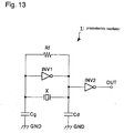
- oscillator 1 is made up of an oscillation stage 2, which comprises a colpitts oscillation circuit consisting of a piezoelectric resonator X, an inverter INV1 for oscillation, a feedback resistor Rf, a capacitor Cg on the gate side, and a capacitor Cd on the drain side, and an output stage 3, which is an inverter INV2 for outputting the oscillation signal.
- Oscillator 1 outputs oscillation pulses P, generated by the oscillation stage 2, through the output stage 3 to an output terminal OUT of the oscillator 1 to which an external load is to be connected.
- Output stage 3 serves to maintain the oscillation stability and avoid frequency deviations of pulses P by preventing the external load from influencing the oscillation stage 2; at the same time, pulses P can be amplified by the output stage 3 to a level suitable for driving the external load.
- the driving power for the inverter INV1 is relatively low.
- the output stage 3 of the oscillator 1 needs to amplify the pulses P to the level suitable for driving the external load, so that the inverter INV2 requires more driving power than inverter INV1.
- FIG. 14 is an example of a circuit structure usable for inverter INV1 and inverter INV2.
- the inverter circuit comprises a series connection of a PMOS transistor and an NMOS transistor with one end of the PMOS transistor connected to a power source terminal VDD and one end of the NMOS transistor connected ground GND; the common gate of the PMOS transistor and the NMOS transistor forms the input G of the inverter and the node at which the respective other ends of the two transistors are connected together is the output D.
- the power noise caused by the inverter INV2 prevents the inverter INV1 from starting stably, thereby resulting in an abnormal oscillation or no oscillation at all of the oscillation stage 2.
- the piezoelectric oscillator 10 illustrated in Fig. 1 has the same structure as the oscillator 1 explained above, except that the configuration of the output stage 13 is different and a start delay circuit is added so as to delay the start of the output stage 13. Hence, the same reference numerals are used for identical parts and those parts will not be explained again.
- FIG. 2 shows the circuit configurations of the output stage 13 and the start delay circuit 14 in more detail.
- the output stage 13 comprises a parallel connection of three clocked gates CG1, CG2 and CG3.
- the clocked gates are each formed of a first and a second PMOS transistor and a first and a second NMOS transistors having their source-drain-paths connected in series in this order between a power source terminal VDD and ground.
- the common gate of the second PMOS transistor and the first NMOS transistor is the input G of the clocked gate and the node between the source-drain-paths of these two transistors is the output D.
- a control input CNT is connected to the gate of the second NMOS transistor and, via an inverter INV3, to the gate of the first PMOS transistor.
- FIG. 4 shows the truth table of the clocked gate.
- control input CNT When control input CNT is at a high level (H), the input signal at input G is inverted at the output D.
- the control input CNT When the control input CNT is at the low level (L), the output D is in a so-called high impedance state regardless of the level at input G.
- the clocked gate switches between an operational state where it operates as a normal inverter and a non-operational state where its output practically becomes open.
- the output stage 13 adds the output pulses from those of the clocked gates CG1 to CG3 whose control input CNT is at a high level, and outputs these added output pulses as pulses P.
- the amplification factor of the output stage 13 as a whole, and, if the output stage 13 is considered to be one (equivalent) inverter IN, the driving power of this inverter change depending on the number of clocked gates whose control input CNT is at a high level.
- While the clocked gates have been described as being made up of MOS transistors they may be made up of bipolar transistors.
- the start delay circuit of output stage 13 consists of a delay circuit 15 for outputting a start signal ⁇ EN, three switches S1, S2 and S3, and a control circuit 16 for controlling the delay circuit 15 and the switches S1 to S3.
- Each of the switches has one end connected to the control input CNT of a respective one of the clocked gates CG1 to CG3; the respective other ends of the switches are commonly connected to the power source terminal VDD.
- the delay circuit 15 consists of a pull-up resistor Rpu having one end connected to the power source terminal VDD, and a parallel circuit of three series connections between the other end of the resistor and ground. Each of the series connections comprises a respective one of three capacitors C1, C2 and C3 and a respective one of three switches Sw1, Sw2 and Sw3.
- the start signal ⁇ EN is taken off the node between the pull-up resistor Rpu and the parallel circuit and is applied to the control circuit 16.
- the level of start signal ⁇ EN gradually increases in accordance with the time constant determined by the resistance of the pull-up resistor Rpu and the capacity of the parallel circuit between the resistor and ground.
- the capacity of the parallel circuit in turn is equal to the sum of the capacities of that or those of capacitors C1 to C3 whose associated switch Sw1, Sw2, and Sw3, respectively, is in the ON state.
- the delay circuit 15 can delay the moment at which the start signal ⁇ EN becomes a high-level signal relative to the moment at which the power supply is turned on by a delay time ⁇ that depends on the connection/disconnection of the switches Sw1 to Sw3.
- each switch S1 to S3 Since one end of each switch S1 to S3 is connected to the power source terminal VDD as described above, a high level signal is supplied to the control input CNT of that or those of the clocked gates CG1 to CG3 whose associated switch is in the ON state.
- the output stage 13 starts amplifying and outputting pulses P and the driving power depends on the number of ON state switches among switches S1 to S3.
- the control circuit 16 By controlling the switches S1 to S3 and the switches Sw1 to Sw3 of the delay circuit 15, the control circuit 16 operates to control the delay circuit 15 and the output stage 13. In other words, when power is supplied from the power source terminal VDD, the control circuit 16 controls the connecting state of switches Sw1 to Sw3 by outputting control signals ⁇ S1, ⁇ S2 and ⁇ S3 to the switches Sw1 to Sw3, respectively, based on set data, which was pre-stored in memory 17. In this way, the control circuit 16 can set the delay time ⁇ .
- control circuit 16 When start signal ⁇ EN has a high level, the control circuit 16 outputs control signals ⁇ Ct1, ⁇ Ct2 and ⁇ Ct3 to the switches S1 to S3, respectively, based on the set data which was pre-stored in the memory 17, thus turning ON a predetermined number of switches. As a result, the control circuit 16 sets the driving power of the output stage 13, and at the same time, the output stage 13 starts operating.
- the control circuit 16 sets the delay time ⁇ for the start signal ⁇ EN based on predetermined set data, and starts the output stage 13 with a predetermined driving power when the delay time ⁇ is over.
- the output stage 13 is started, delayed by a predetermined delay time ⁇ relative to the oscillation stage 2, which starts right after the power supply is turned on.
- the control circuit 16 has input terminals CNT1, CNT2 and CNT3 for inputting set data, and another input terminal OE for inputting a stop signal ⁇ OE for stopping operation of the output stage 13. More specifically, when set data is input through the input terminals CNT1 to CNT3, the set data stored in the memory 17 is renewed to the set data thus supplied. As a result, oscillator 10 allows changing the delay time ⁇ as well as changing the driving power of the output stage 13. While the set data for controlling the switches Sw1 to Sw3 and the switches S1 to S3 are shown to be input as parallel data via the three input terminals CNT1 to CNT3, there may be just one input terminal for inputting set data as serial data.
- the control circuit 16 stops the operation of the output stage 13 by turning the switches S1 to S3 off. Therefore, the oscillator 10 can be made to stop outputting the pulses P at any desirable timing determined by the user of the oscillator 10.
- data is set at an adjustment circuit 20 so as to set the ON/OFF state for each of the switches S1 to S3 and Sw1 to Sw3 by operating the external adjustment circuit 20.
- the switches S1 to S3 are principally set so as to obtain the driving power necessary for the output stage 13.
- the ON/OFF states of the switches Sw1 to Sw3, in other words, the delay time ⁇ , should be set so that the output stage 13 starts operating at a time at which the oscillation of the oscillation stage 2 has stabilized and is no longer affected by the power noise generated when the output stage 13 starts operating. Therefore, the delay time ⁇ must be established corresponding to the starting properties of the inverter INV1 of the oscillation stage 2, the driving power of the output stage 3 and the like. Thus, which of the switches Sw1 to Sw3 is to be turned on, is appropriately confirmed depending on whether there is any abnormal oscillation or no oscillation at all, while the output signal of the oscillator 10 is being monitored.
- the set data stored or set in adjustment circuit 20 is supplied to the control circuit 16 through the terminals CNT1 to CNT3, thus overwriting set data in memory 17, if any.
- the set data in memory 17 can be renewed to new set data before the oscillation stage 2 starts oscillating.
- the starting property of the oscillator 10, based on new set data, can then be monitored immediately.
- set data can be recorded in memory 17 before the oscillation stage 2 starts oscillating; thus, even if no set data have yet been recorded in the memory 17, a malfunction of the oscillator 10 caused by a lack of set data can be avoided.
- the appropriate delay time can be selected and set.
- the memory 17 of the control circuit 16 may be a non-volatile memory, which can be written only once.
- the control circuit 16 controls switches Sw1 to Sw3 based on the set data kept at the adjustment circuit 20, instead of the set data stored in memory 17. After an appropriate delay time ⁇ has been established, corresponding set data is recorded in the memory 17, thus setting the appropriate delay time ⁇ .
- the oscillator 10 starts the output stage 13 later than the oscillation stage 2 by a predetermined delay time ⁇ , so that the starting property of the oscillation stage 2 can be stabilized by avoiding power noise being generated at the output stage 13 while the oscillation stage starts oscillating; hence, the oscillation stability of oscillation pulse can be improved.
- the output stage 13 is configured by connecting a plurality of clocked gates in parallel, so that the driving power of the output stage 13 can be selected among multiple values as desired by the user.
- three series connections i.e., three pairs of capacitor and switch are provided to change the delay time ⁇ of the delay circuit 15.
- the present invention is not limited to this case.
- the number of such pairs of capacitor and switch may be increased or decreased depending on the necessary number of candidate delay times.
- the number of clocked gates, constituting the output stage 13 may also be increased or decreased. In this case, the number of switches for controlling the clocked gates would be increased or decreased correspondingly.
- the delay circuit 15 consists of one pull-up resistor Rpu, a plurality of capacitors C1 to C3, and switches Sw1 to Sw3.
- the present invention is not limited to this case, and can broadly apply circuits, whose time constants change in response to the connection state of one or more switches.
- the number of elements of the delay circuit 15 may be reduced, and the circuit configuration may be simplified.
- control circuit 16 starts the output stage 13 by means of switches S1 to S3, but the present invention is not limited to this case.
- start signal EN may be supplied to the control input CNT of each clocked gate of the output stage 13 so as to directly start the output stage 13 by the start signal ⁇ EN.
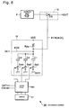
- FIG. 9 is a circuit diagram of oscillator 40 in which the output stage 13 is controlled directly by the start signal ⁇ EN and the stop signal ⁇ OE, wherein the delay circuit 15 has the same structure as that in the second modified embodiment of Fig. 6.
- the control circuit should maintain the switches (corresponding to S1 to Sn in Fig. 1 but not shown in this simplified example) connected to control input CNT of the clocked gates in the number corresponding to obtain the necessary driving power for the output stage 13, in the ON state before the output stage 13 is started.
- a configuration can be considered wherein the switches of the delay circuit 15 and the switches connected to the control inputs CNT of the clocked gates of the output stage 13 correspond to each other, and a switch connected to the control input CNT of the corresponding clocked gate, will be turned ON when the switch of the delay circuit 15 is turned ON.
- start signal ⁇ EN and stop signal ⁇ OE may be directly supplied to the clocked gates.
- the control circuit 16A is only to control the switches of the delay circuit 15, and the configuration of the control circuit 16A may be simplified.
- the output stage 13 is directly controlled to stop operating by the stop signal ⁇ OE as with the oscillator 30 shown in FIG. 8, it is preferable to turn OFF all the switches of the delay circuit 15 after the oscillator 30 is completed to oscillate or has reached a steady state, in order to make the response to the stop signal ⁇ OE faster.
- the stop signal ⁇ OE is directly supplied to the output stage 13 through the input terminal OE, a resistor for setting the electric potential of the terminal OE is necessary so as to avoid the potential from floating when the circuit providing the signal ⁇ OE is in the open state.
- the pull-up resistor Rpu is used as such resistor in the embodiment of FIG. 8. Since, in the embodiment of FIG. 8, the output stop signal ⁇ OE and the start signal ⁇ EN are applied to the same control input terminal of output stage 13, the pull-up resistor Rpu prevents the potential at input terminal OE from floating and no additional resistor is required.
- the pull-up capability in other words, the stability of terminal voltage, improves.
- a low-level signal is applied to the input terminal OE as stop signal, a current path is formed from the power source terminal VDD to ground GND through these pull-up resistors, which is not preferable from the standpoint of energy efficiency. Therefore, even from the standpoint of energy efficiency, it is preferable to disconnect the pull-up resistors Rpu1 to Rpum by turning OFF all the switches Swj of the delay circuit after the oscillator 40 is completed oscillating or reached a steady state.
- a plurality of capacitors or pull-up resistors whose connection/disconnection is controlled by switches are connected in parallel in the delay circuit 15.
- the present invention is not limited to this case, and a plurality of capacitors or pull-up resistors whose connection/disconnection is controlled by switches, may be connected in series, instead.
- FIG. 10 is a block diagram of a piezoelectric oscillator 50 in which the delay circuit 15 is configured by connecting capacitors Cj (wherein j is 1, 2, ..., m) in series via changeover switches SWj connecting, under the control of control circuit 16, an associated capacitor either to another capacitor or to ground.
- capacitor C1 has one end connected to pull-up resistor Rpu and the other end connected to a movable contact of switch Sw1.
- Switch Sw1 connects capacitor C1 either to ground or to one end of capacitor C2.
- the other end of capacitor C2 is connected to a movable contact of switch Sw2 for connecting capacitor C2 either to ground or to capacitor C3.
- a desirable number of capacitor/switch combinations may be connected in series. In this case, when the delay time of the start signal ⁇ EN is set to be long, the number of capacitors to be connected in series is reduced.
- the delay time ⁇ of the start signal ⁇ EN is set preferably by using the delay circuit 15, whose time constant varies depending on the connection state of a plurality of mechanical or electronic switches.
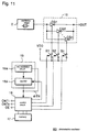
- the delay circuit 15 may be made up of an oscillation circuit 15a and a counter 15b as shown in FIG. 11.
- an RC oscillation circuit 1 5a generates pulses as soon as the power supply to the piezoelectric oscillator 60 is turned on, and the counter 15b counts these pulses.
- the count value of the counter 15b reaches a pre-set value
- high-level start signal ⁇ EN is output.
- start signal ⁇ EN is also used here to stop operation of the RC oscillation circuit 15a.
- the oscillator can surely oscillate and provide pulses while lowering the power noise during the transient period after power supply was turned on, so that the elements, constituting the oscillator, can be integrated.
- the whole circuit of the oscillator except for the resonator may be integrated (an integrated circuit), and provided in one ceramic package or a plastic package.
- the oscillator may be miniaturized and the number of parts can be reduced, thus reducing the assembly man-hours and manufacturing costs.
- a piezoelectric oscillator can be broadly used for a variety of devices, such as a radio communication device and an electronic device.
- An oscillator which is built in a portable radio communication device, carries out intermittent oscillation during intermittent reception so as to save batteries, so that abnormal oscillations or no oscillation is usually a problem. Therefore, the oscillator according to the present invention is particularly suitable for a portable radio communication device.
Landscapes
- Chemical & Material Sciences (AREA)
- Crystallography & Structural Chemistry (AREA)
- Oscillators With Electromechanical Resonators (AREA)
Abstract
Description
- FIG. 1
- is a block diagram of an oscillator according to a basic embodiment of the present invention;
- FIG. 2
- shows the circuit configuration of the output stage and the start delay circuit;
- FIG. 3
- illustrates an example of a clocked gate;
- FIG. 4
- is a truth table of the clocked gate;
- FIG. 5
- is a diagram for explaining the setting of the delay time;
- FIG. 6 to 11
- are block diagrams of respective oscillators according modified embodiments of the invention;
- FIG. 12
- is a block diagram of a conventional piezoelectric oscillator for use in an electronic device;
- FIG. 13
- illustrates the circuit structure of the oscillator; and
- FIG. 14
- shows the circuit structure of an inverter used for the oscillation stage and the output stage.
Claims (16)
- A piezoelectric oscillator comprising:characterized by start delay means responsive to electric power to the oscillator being turned on for delaying the start of operation of the output stage (13) relative to that of the oscillation stage (2) by a delay time selected from a plurality of available delay times.an oscillation stage (2) for generating pulses by exciting a piezoelectric resonator; andan output stage (13) for amplifying the pulses and outputting the amplified pulses;
- The oscillator according to Claim 1, wherein the start delay means comprises:selection means (16, 17) for selecting one delay time from the plurality of delay times based on pre-set information;delay means (15) for generating a start signal (EN) gradually changing from a first level to a second level in accordance with the selected delay time; andstarting means (16, 17, S1-S3) for causing the output stage (13) to start in response to the start signal reaching its second level.
- The oscillator according to Claim 1, wherein the start delay means comprises:wherein the output stages (13) is adapted to start operating in response to the start signal reaching its second level.selection means (16A, 17) for selecting one delay time from the plurality of delay times based on pre-set information; anddelay means for generating a start signal (EN) gradually changing from a first level to a second level in accordance with the selected delay time and for applying the start signal to the output stage (13);
- The oscillator according to Claim 2 or Claim 3, wherein the delay means comprises:wherein the selection means (16, 17; 16A, 17) is adapted to select said delay time by controlling the plurality of switching means based on said pre-set information.a resistance element (Rpu);a plurality of capacitance elements (C1-C3); anda plurality of switching means (Sw1-Sw3, Sw1-Swm) connected to the plurality of capacitance elements, respectively;
- The oscillator according to Claim 2 or Claim 3, wherein the delay means comprises:wherein the selection means (16, 17) is adapted to select said delay time by controlling the plurality of switching means based on said pre-set information.a capacitance element (C);a plurality of resistance elements (Rpu1-Rpum); anda plurality of switching means (Sw1-Swm) connected to the plurality of resistance elements, respectively;
- The oscillator according to Claim 5, wherein the switching means are transistors (Tr1-Trm), and the resistance elements are the ON resistances of the transistors.
- The oscillator according to Claim 1, wherein the start delay means comprises:selection means (16, 17) for selecting one delay time from the plurality of delay times based on pre-set information;delay means (15) for generating a start signal (EN) at a time delayed by the selected delay time from the start of oscillation of the oscillation stage (2); anda starting means (S1-Sn) for causing the output stage (13) to start in response to the start signal.
- The oscillator according to Claim 1, wherein the start delay means comprises:wherein the output stage is adapted to start operating in response to the start signal.selection means for selecting one delay time from the plurality of delay times based on pre-set information; anddelay means for generating a start signal at a time delayed by the selected delay time from the start of oscillation of the oscillation stage and for applying the start signal to the output stage;
- The oscillator according to Claim 7 or Claim 8, wherein the delay means (15) comprises:an oscillation circuit (2; 15a) for generating pulses; anda counter (15b) for counting the pulses generated by said oscillation circuit and for outputting said start signal (EN) when a predetermined number of pulses has been counted; wherein the selection means (16, 17) is adapted to set said predetermined number corresponding to the selected delay time based on said pre-set information.
- The oscillator according to Claim 9, wherein the oscillation circuit is the oscillation stage (2).
- The oscillator according to any of Claim 2 to Claim 7, wherein the output stage (13) comprises a plurality of clocked gates (CG1-CG3) connected in parallel; and wherein the starting means (S1-S3; S1-Sn) is adapted to cause the output stage (13) to start operating by operating predetermined clocked gates among the plurality of clocked gates based on pre-set information.
- The oscillator according to any of Claim 2 to Claim 11, wherein the selection means (16, 17; 16A, 17) has input terminal means (CNT1, CNT2) for inputting information so as to renew said pre-set information to new set information as the new set information is input via the input terminal means.
- The oscillator according to any of Claim 2, Claim 7 and Claim 11 wherein the starting means (S1-S3; S1-Sn) has a control input terminal (OE) and the output stage (13) is adapted to stop operating in response to a stop signal (OE) being applied to the control input terminal.
- The oscillator according to any of Claim 1 to Claim 13 wherein, except for a piezoelectric resonator, the circuit of the oscillator is integrated.
- The oscillator according to Claim 14 wherein the oscillator is housed in one package.
- An electronic device, having the oscillator according to any of Claim 1 to Claim 15, and operating based on the pulses (P) output from the oscillator.
Applications Claiming Priority (2)
| Application Number | Priority Date | Filing Date | Title |
|---|---|---|---|
| JP32879299 | 1999-11-18 | ||
| JP32879299A JP2001148612A (en) | 1999-11-18 | 1999-11-18 | Piezoelectric oscillator and electronic equipment |
Publications (3)
| Publication Number | Publication Date |
|---|---|
| EP1102391A2 true EP1102391A2 (en) | 2001-05-23 |
| EP1102391A3 EP1102391A3 (en) | 2002-02-06 |
| EP1102391B1 EP1102391B1 (en) | 2003-06-04 |
Family
ID=18214170
Family Applications (1)
| Application Number | Title | Priority Date | Filing Date |
|---|---|---|---|
| EP00123957A Expired - Lifetime EP1102391B1 (en) | 1999-11-18 | 2000-11-03 | Piezoelectric oscillator and electronic device using it |
Country Status (4)
| Country | Link |
|---|---|
| US (1) | US6480071B1 (en) |
| EP (1) | EP1102391B1 (en) |
| JP (1) | JP2001148612A (en) |
| DE (1) | DE60003138T2 (en) |
Cited By (2)
| Publication number | Priority date | Publication date | Assignee | Title |
|---|---|---|---|---|
| US6480071B1 (en) * | 1999-11-18 | 2002-11-12 | Seiko Epson Corporation | Piezoelectric oscillator and electronic device |
| EP1328065A3 (en) * | 2002-01-10 | 2005-07-20 | Fujitsu Limited | Oscillator circuits |
Families Citing this family (12)
| Publication number | Priority date | Publication date | Assignee | Title |
|---|---|---|---|---|
| DE10126608A1 (en) * | 2001-05-31 | 2002-12-12 | Infineon Technologies Ag | Compensated oscillator circuit |
| DE10154812B4 (en) * | 2001-11-08 | 2010-04-15 | Qimonda Ag | Circuit for adjusting a signal propagation time of a signal on a signal line |
| JP2006157767A (en) * | 2004-12-01 | 2006-06-15 | Renesas Technology Corp | Communication semiconductor integrated circuit with built-in oscillation circuit, communication system, and manufacturing method of semiconductor integrated circuit |
| US7558086B2 (en) * | 2006-06-28 | 2009-07-07 | Zippy Technology Corp. | Inverter control circuit with a resonant frequency modulation function |
| US7420432B2 (en) * | 2006-07-11 | 2008-09-02 | Mediatek Inc. | Noise removal circuit |
| JP2009290380A (en) * | 2008-05-27 | 2009-12-10 | Kyocera Kinseki Corp | Oscillator |
| JP5311545B2 (en) * | 2008-05-27 | 2013-10-09 | 京セラクリスタルデバイス株式会社 | Oscillator |
| JP2011217349A (en) * | 2010-03-19 | 2011-10-27 | Panasonic Corp | Crystal oscillator circuit |
| US8164392B2 (en) * | 2010-04-26 | 2012-04-24 | Juniper Networks, Inc. | Error-free startup of low phase noise oscillators |
| US9515604B2 (en) | 2014-05-19 | 2016-12-06 | Texas Instruments Incorporated | Driving crystal oscillator startup at above, below and operating frequency |
| CN105739660A (en) * | 2014-12-10 | 2016-07-06 | 鸿富锦精密工业(武汉)有限公司 | Voltage regulation device of electronic equipment |
| RU2627716C2 (en) * | 2015-12-03 | 2017-08-10 | Лев Антонович Симонов | Radiation hard circuit of quartz generator frequency resetting with non-volatile memory |
Family Cites Families (8)
| Publication number | Priority date | Publication date | Assignee | Title |
|---|---|---|---|---|
| JPS57103408A (en) | 1980-12-19 | 1982-06-28 | Hitachi Ltd | Quartz oscillator circuit |
| JPS5860806A (en) | 1981-10-06 | 1983-04-11 | Toshiba Corp | Semiconductor device |
| JPS59169301A (en) | 1983-03-16 | 1984-09-25 | Hitachi Ltd | Controller of motor driven blower for electric rolling stock |
| US5126695A (en) | 1989-06-14 | 1992-06-30 | Seiko Epson Corporation | Semiconductor integrated circuit device operated with an applied voltage lower than required by its clock oscillator |
| JPH0481009A (en) | 1990-07-20 | 1992-03-13 | Seiko Epson Corp | Piezoelectric oscillation circuit |
| JPH0548440A (en) | 1991-08-09 | 1993-02-26 | Seiko Epson Corp | Semiconductor integrated circuit |
| US5568100A (en) | 1995-09-22 | 1996-10-22 | Lucent Technologies Inc. | Synchronous power down clock oscillator device |
| JP2001148612A (en) * | 1999-11-18 | 2001-05-29 | Seiko Epson Corp | Piezoelectric oscillator and electronic equipment |
-
1999
- 1999-11-18 JP JP32879299A patent/JP2001148612A/en not_active Withdrawn
-
2000
- 2000-10-31 US US09/699,421 patent/US6480071B1/en not_active Expired - Lifetime
- 2000-11-03 EP EP00123957A patent/EP1102391B1/en not_active Expired - Lifetime
- 2000-11-03 DE DE60003138T patent/DE60003138T2/en not_active Expired - Lifetime
Cited By (5)
| Publication number | Priority date | Publication date | Assignee | Title |
|---|---|---|---|---|
| US6480071B1 (en) * | 1999-11-18 | 2002-11-12 | Seiko Epson Corporation | Piezoelectric oscillator and electronic device |
| EP1328065A3 (en) * | 2002-01-10 | 2005-07-20 | Fujitsu Limited | Oscillator circuits |
| US7042300B2 (en) | 2002-01-10 | 2006-05-09 | Fujitsu Limited | Oscillator circuit, semiconductor device and semiconductor memory device provided with the oscillator circuit, and control method of the oscillator circuit |
| US7239210B2 (en) | 2002-01-10 | 2007-07-03 | Fujitsu Limited | Oscillator circuit, semiconductor device and semiconductor memory device provided with the oscillator circuit, and control method of the oscillator circuit |
| US7492232B2 (en) | 2002-01-10 | 2009-02-17 | Fujitsu Microelectronics Limited | Oscillator circuit, semiconductor device and semiconductor memory device provided with the oscillator circuit, and control method of the oscillator circuit |
Also Published As
| Publication number | Publication date |
|---|---|
| EP1102391B1 (en) | 2003-06-04 |
| JP2001148612A (en) | 2001-05-29 |
| US6480071B1 (en) | 2002-11-12 |
| EP1102391A3 (en) | 2002-02-06 |
| DE60003138D1 (en) | 2003-07-10 |
| DE60003138T2 (en) | 2004-01-29 |
Similar Documents
| Publication | Publication Date | Title |
|---|---|---|
| EP1102391B1 (en) | Piezoelectric oscillator and electronic device using it | |
| US6563391B1 (en) | Precision crystal oscillator circuit used in microcontroller | |
| US5117206A (en) | Variable capacitance integrated circuit usable in temperature compensated oscillators | |
| US6285264B1 (en) | Crystal oscillator with frequency trim | |
| US7852164B2 (en) | Piezoelectric oscillator | |
| US4321562A (en) | Crystal oscillator circuit capable of changing the number of inverter stages coupled in series | |
| JP2008054134A (en) | RING OSCILLATOR, SEMICONDUCTOR INTEGRATED CIRCUIT AND ELECTRONIC DEVICE HAVING THE SAME | |
| US20130038505A1 (en) | Semiconductor device and radio communication device | |
| JP2002344242A (en) | Voltage-controlled oscillator | |
| JP3201339B2 (en) | Oscillation circuit | |
| US8890632B2 (en) | Oscillator circuit | |
| US9634608B2 (en) | Crystal oscillation circuit and electronic timepiece | |
| EP2242175B1 (en) | Oscillator circuit | |
| EP1187309B1 (en) | Voltage-controlled oscillator, IC chip for voltage-controlled oscillator, resistance setting apparatus, and resistance setting method | |
| JP3937781B2 (en) | Crystal oscillation circuit | |
| US20070126485A1 (en) | Voltage-controlled oscillator | |
| US5770979A (en) | Programmable oscillator using one capacitor | |
| JP2022170966A (en) | circuit devices and oscillators | |
| JP2003283249A (en) | Crystal oscillation circuit and electronic equipment using the crystal oscillation circuit | |
| US11664765B2 (en) | Circuit device and oscillator | |
| JP2005217773A (en) | Voltage controlled piezoelectric oscillator | |
| US6690245B2 (en) | Oscillation control circuit | |
| JP2007053746A (en) | Integrated circuit | |
| JPH06140838A (en) | Crystal oscillator | |
| JP7845544B2 (en) | Oscillator, oscillator, and control method for the oscillator |
Legal Events
| Date | Code | Title | Description |
|---|---|---|---|
| PUAI | Public reference made under article 153(3) epc to a published international application that has entered the european phase |
Free format text: ORIGINAL CODE: 0009012 |
|
| AK | Designated contracting states |
Kind code of ref document: A2 Designated state(s): DE FR GB Kind code of ref document: A2 Designated state(s): AT BE CH CY DE DK ES FI FR GB GR IE IT LI LU MC NL PT SE TR |
|
| AX | Request for extension of the european patent |
Free format text: AL;LT;LV;MK;RO;SI |
|
| PUAL | Search report despatched |
Free format text: ORIGINAL CODE: 0009013 |
|
| AK | Designated contracting states |
Kind code of ref document: A3 Designated state(s): AT BE CH CY DE DK ES FI FR GB GR IE IT LI LU MC NL PT SE TR |
|
| AX | Request for extension of the european patent |
Free format text: AL;LT;LV;MK;RO;SI |
|
| 17P | Request for examination filed |
Effective date: 20020522 |
|
| AKX | Designation fees paid |
Free format text: DE FR GB |
|
| GRAH | Despatch of communication of intention to grant a patent |
Free format text: ORIGINAL CODE: EPIDOS IGRA |
|
| GRAH | Despatch of communication of intention to grant a patent |
Free format text: ORIGINAL CODE: EPIDOS IGRA |
|
| GRAH | Despatch of communication of intention to grant a patent |
Free format text: ORIGINAL CODE: EPIDOS IGRA |
|
| GRAA | (expected) grant |
Free format text: ORIGINAL CODE: 0009210 |
|
| AK | Designated contracting states |
Designated state(s): DE FR GB |
|
| REG | Reference to a national code |
Ref country code: GB Ref legal event code: FG4D |
|
| REG | Reference to a national code |
Ref country code: IE Ref legal event code: FG4D |
|
| REF | Corresponds to: |
Ref document number: 60003138 Country of ref document: DE Date of ref document: 20030710 Kind code of ref document: P |
|
| ET | Fr: translation filed | ||
| PLBE | No opposition filed within time limit |
Free format text: ORIGINAL CODE: 0009261 |
|
| STAA | Information on the status of an ep patent application or granted ep patent |
Free format text: STATUS: NO OPPOSITION FILED WITHIN TIME LIMIT |
|
| 26N | No opposition filed |
Effective date: 20040305 |
|
| REG | Reference to a national code |
Ref country code: IE Ref legal event code: MM4A |
|
| REG | Reference to a national code |
Ref country code: FR Ref legal event code: PLFP Year of fee payment: 16 |
|
| PGFP | Annual fee paid to national office [announced via postgrant information from national office to epo] |
Ref country code: GB Payment date: 20151028 Year of fee payment: 16 Ref country code: DE Payment date: 20151028 Year of fee payment: 16 |
|
| PGFP | Annual fee paid to national office [announced via postgrant information from national office to epo] |
Ref country code: FR Payment date: 20151008 Year of fee payment: 16 |
|
| REG | Reference to a national code |
Ref country code: DE Ref legal event code: R119 Ref document number: 60003138 Country of ref document: DE |
|
| GBPC | Gb: european patent ceased through non-payment of renewal fee |
Effective date: 20161103 |
|
| REG | Reference to a national code |
Ref country code: FR Ref legal event code: ST Effective date: 20170731 |
|
| PG25 | Lapsed in a contracting state [announced via postgrant information from national office to epo] |
Ref country code: FR Free format text: LAPSE BECAUSE OF NON-PAYMENT OF DUE FEES Effective date: 20161130 |
|
| PG25 | Lapsed in a contracting state [announced via postgrant information from national office to epo] |
Ref country code: DE Free format text: LAPSE BECAUSE OF NON-PAYMENT OF DUE FEES Effective date: 20170601 Ref country code: GB Free format text: LAPSE BECAUSE OF NON-PAYMENT OF DUE FEES Effective date: 20161103 |