EP1102343A1 - Polarized wave separator - Google Patents
Polarized wave separator Download PDFInfo
- Publication number
- EP1102343A1 EP1102343A1 EP00310324A EP00310324A EP1102343A1 EP 1102343 A1 EP1102343 A1 EP 1102343A1 EP 00310324 A EP00310324 A EP 00310324A EP 00310324 A EP00310324 A EP 00310324A EP 1102343 A1 EP1102343 A1 EP 1102343A1
- Authority
- EP
- European Patent Office
- Prior art keywords
- wave
- partition wall
- polarized wave
- waveguide
- substrate
- Prior art date
- Legal status (The legal status is an assumption and is not a legal conclusion. Google has not performed a legal analysis and makes no representation as to the accuracy of the status listed.)
- Granted
Links
Images












Classifications
-
- H—ELECTRICITY
- H01—ELECTRIC ELEMENTS
- H01P—WAVEGUIDES; RESONATORS, LINES, OR OTHER DEVICES OF THE WAVEGUIDE TYPE
- H01P1/00—Auxiliary devices
- H01P1/16—Auxiliary devices for mode selection, e.g. mode suppression or mode promotion; for mode conversion
- H01P1/161—Auxiliary devices for mode selection, e.g. mode suppression or mode promotion; for mode conversion sustaining two independent orthogonal modes, e.g. orthomode transducer
Definitions
- the present invention relates to polarized wave separators, and more particularly to a polarized wave separator for use in a receiving converter (a low noise blockdown converter, LNB) that receives radio wave from a broadcasting or communication satellite.
- a receiving converter a low noise blockdown converter, LNB
- Microwave being used in satellite broadcasting normally consists of two components.
- circularly polarized wave includes clockwise polarized wave and counterclockwise polarized wave.
- Linearly polarized wave includes vertically polarized wave and horizontally polarized wave.
- the receiving converter is required to efficiently separate such two components from each other, and a polarized wave separator is used for such separation of microwave.
- a polarized wave separator for use in the receiving converters, a polarized wave separator for separating the components included in circularly polarized wave will now be described.
- a pair of wave receiving probes 104a, 104b is formed on a substrate 103.
- a waveguide 101 is placed on one side of substrate 103.
- a waveguide partition wall lOla in a stepped shape is formed within waveguide 101, which partitions the interior of waveguide 101 into two portions.
- a wave reflecting unit 102 is placed on the other side of substrate 103.
- a wave reflecting unit partition wall 102a is formed within wave reflecting unit 102, which partitions the interior thereof into two portions.
- a wave reflecting surface 102b is formed on an end surface of wave reflecting unit 102 opposite to substrate 103.
- an earthed surface (pattern) 105 is formed along end surfaces of wave reflecting unit 102 and its partition wall 102a such that they contact with each other.
- another earthed surface is formed along end surfaces of waveguide 101 and its partition wall lOla such that they contact with each other.
- the earthed surface 105 for contact with wave reflecting unit 102 and the earthed surface for contact with waveguide 101 are electrically connected to each other via a through hole 106.
- waveguide 101 and wave reflecting unit 102 are both maintained at an earth potential via substrate 103.
- the pair of wave receiving probes 104a, 104b is formed on substrate 103 on its side facing wave reflecting unit 102. Interconnection portions of wave receiving probes 104a, 104b are electrically isolated from any of earthed surface 105, wave receiving unit 102 and waveguide 101.
- Waveguide partition wall lOla and wave reflecting unit partition wall 102a act to partition the interior of waveguide 101 and wave reflecting unit 102, respectively, into two wave-guiding spaces. Circularly polarized wave caught within waveguide 101 is separated by waveguide partition wall 101a and introduced into respective wave-guiding spaces.
- the conventional polarized wave separators have configurations as described above.
- the wave may escape fiom waveguide 101, or the wave may not be separated successfully.
- wave reflecting unit 102 and waveguide 101 are electrically connected to each other via substrate 103, there may arise a problem that the wave introduced into waveguide 101 will be attenuated by substrate 103 before reaching wave reflecting surface 102b, which results in further weakening of the wave.
- wave loss such reduction in strength of the wave due to escape and/or attenuation will be referred to as "wave loss”.
- An object of the present invention is to provide a polarized wave separator that ensures separation of radio wave while suppressing escape of the wave, thereby reducing the wave loss.
- a polarized wave separator includes a substrate portion, a pair of wave receiving portions, a waveguide, and a wave reflecting unit.
- the substrate has an opening portion.
- the pair of wave receiving portions is formed on the substrate on opposite sides in a radial direction of the opening portion.
- the waveguide is located on one side of the substrate portion, and has a partition wall portion provided therein.
- the wave reflecting unit is located on the other side of the substrate portion, and has a wave reflecting surface formed on its inner side.
- the waveguide, substrate portion and wave reflecting unit together form a wave-guiding space.
- the partition wall portion extends through the opening portion to the wave reflecting unit, and divides the wave reflecting surface into two portions. By the partition wall, the wave-guiding space is partitioned into two spaces, one in which one of the pair of wave receiving portions is located and the other in which the other of the pair of wave receiving portions is located.
- the wave-guiding space formed by the waveguide, substrate and wave reflecting unit is partitioned by the single partition wall penetrating the opening formed on the substrate. Therefore, the separated wave caught in the respective wave-guiding spaces is prevented from escaping from one wave-guiding space to the other wave-guiding space both in the waveguide and in the wave reflecting unit near the substrate portion. This improves polarized wave-separating characteristics.
- the wave guided in the wave-guiding spaces is propagated to the wave reflecting surface without being interrupted by the substrate portion. This reduces the wave loss.
- the substrate portion is contacted only by the tubular portion of the wave reflecting unit and the waveguide, so that they both can make good contact with the substrate.
- the substrate portion is contacted only by the tubular portion of the wave reflecting unit and the waveguide, so that they both can make good contact with the substrate.
- the waveguide is located such that the internal circumference of the waveguide encircles the opening portion.
- the wave reflecting unit includes the tubular portion that is located on the other side of the substrate portion from the waveguide, and an end surface portion that is located on an end of the tubular portion where a wave reflecting surface is formed.
- the partition wall portion contacts at least the end surface portion, so that it is electrically connected with the wave reflecting unit.
- the end portion of the partition portion facing the wave reflecting surface is preferably in a convex shape, and this convex shaped end portion contacts the wave reflecting surface.
- a groove portion is formed on an inner side of the end surface portion of the wave reflecting unit, so that the end portion of the partition wall portion facing the wave reflecting surface is accepted in the groove portion.
- the end portion of the partition wall portion is in a saw-tooth waveform or a waveform, and the groove portion is formed in a shape corresponding thereto. This assures the contact between the partition wall portion and the wave reflecting unit.
- the end surface portion of the wave reflecting unit is provided with a female screw portion and a male screw portion mounted onto the female screw portion, and the male screw portion contacts the partition wall portion.
- a slit portion is formed on the end surface portion which penetrates the end surface portion, and the end portion of the partition wall portion facing the wave reflecting surface is inserted into the slit portion.
- the end portion of the partition wall portion penetrates the slit portion and is riveted at the outside of the end surface portion.
- a conductive member is mounted between the end portion of the partition wall portion and the slit portion.
- the conductive member preferably includes an elastic body or a resin.
- the end portion of the partition wall portion penetrates the slit portion and is exposed at the end surface portion, and a conductive member is formed to directly cover the end surface portion and the exposed end portion.
- the conductive member preferably includes a conductive film, metal foil, conductive paste or conductive adhesive.
- the end portion of the partition wall portion penetrates the slit portion and is exposed at the end surface portion, and the end surface portion and the exposed end portion are welded.
- the partition wall portion contacts the tubular portion, and at the portion where the tubular portion and the partition wall portion contact with each other, a concave portion is provided to either one of the tubular portion and the partition wall portion that is formed along a direction in which the partition wall portion extends, and a convex portion is provided to the other of the tubular portion and the partition wall portion that is fitted into the concave portion.
- a conductive, earthed cap portion is provided between the partition wall portion and the slit portion to cover the end portion.
- provision of such earthed cap portion ensures that the partition wall portion and the end portion are electrically conducted to each other.
- the earthed cap portion includes a side portion that is formed towards a direction in which the partition wall portion extends, and a cut and bent portion that is bent towards the slit portion side or towards the partition wall portion side.
- the cut and bent portion further ensures the electrical conduction between the partition wall portion and the end surface portion, and also prevents the earthed cap portion from falling off.
- the earthed cap portion includes a hooked portion that closely contacts the wave reflecting surface of the end surface portion.
- the earthed cap portion is secured on the wave reflecting surface, so that it is reliably mounted in the slit portion.
- Fig. 1 is a perspective view of a polarized wave separator before assembly according to a first embodiment of the present invention.
- Fig. 2 is a cross sectional view taken along a line II-II of Fig. 1.
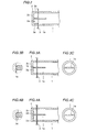
- Fig. 3A is a partial, vertical sectional view of a polarized wave separator according to a second embodiment of the present invention.
- Fig. 3B is a partial, enlarged sectional view of the polarized wave separator of Fig. 3A.
- Fig. 3C is a side view of the polarized wave separator of Fig. 3A.
- Fig. 4A is a partial, vertical sectional view of a polarized wave separator according to a third embodiment of the present invention.
- Fig. 4B is a partial, enlarged sectional view of the polarized wave separator of Fig. 4A.
- Fig. 4C is a side view of the polarized wave separator of Fig. 4A.
- Fig. 5A is a partial, vertical sectional view of a polarized wave separator according to a fourth embodiment of the present invention.
- Fig. 5B is a partial, sectional view taken along a line VB-VB of Fig. 5A.
- Fig. 5C is a partial, enlarged sectional view of the polarized wave separator of Fig. 5A.
- Fig. 5D is a partial, enlarged sectional view of a modification of the polarized wave separator of Fig. 5A.
- Fig. 6A is a partial, vertical sectional view of a polarized wave separator according to a fifth embodiment of the present invention.
- Fig. 6B is a partial, enlarged sectional view of the polarized wave separator of Fig. 6A.
- Fig. 6C is a partial, vertical sectional view of the polarized wave separator of Fig. 6A before formation of a riveted portion.
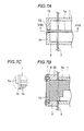
- Fig. 7A is a partial, vertical sectional view of a polarized wave separator according to a sixth embodiment of the present invention.
- Fig. 7B is a partial, sectional view taken along a line VIIB-VIIB of Fig. 7A.
- Fig. 7C is a partial, enlarged sectional view of the polarized wave separator of Fig. 7A.
- Fig. 8A is a partial, vertical sectional view of a polarized wave separator according to a seventh embodiment of the present invention.
- Fig. 8B is a partial, sectional view taken along a line VIIIB-VIIIB of Fig. 8A.
- Fig. 8C is a partial, enlarged sectional view of the polarized wave separator of Fig. 8A.
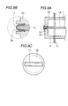
- Fig. 9A is a partial, vertical sectional view of a polarized wave separator according to an eighth embodiment of the present invention.
- Fig. 9B is a partial, enlarged sectional view of the polarized wave separator of Fig. 9A.
- Fig. 9C is a side view of the polarized wave separator of Fig. 9A.
- Fig. 10A is a partial, vertical sectional view of a polarized wave separator according to a ninth embodiment of the present invention.
- Fig. 10B is a partial, enlarged sectional view of the polarized wave separator of Fig. 10A.
- Fig. 10C is a side view of the polarized wave separator of Fig. 10A.
- Fig. 11A is a partial, vertical sectional view of a modification of the polarized wave separator according to the ninth embodiment.
- Fig. 11B is a partial, enlarged sectional view of the polarized wave separator of Fig. 11A.
- Fig. 11C is a side view of the polarized wave separator of Fig. 11A.
- Fig. 12A is a partial, vertical sectional view of a polarized wave separator according to a tenth embodiment of the present invention.
- Fig. 12B is a partial, enlarged sectional view of the polarized wave separator of Fig. 12A.
- Fig. 12C is a partial, vertical sectional view of the polarized wave separator of Fig. 12A before formation of a welded portion.
- Fig. 13A is a partial, vertical sectional view of a polarized wave separator according to an eleventh embodiment of the present invention.
- Fig. 13B is a partial, sectional view taken along a line XIIIB-XIIIB of Fig. 13A.
- Fig. 13C is a partial, enlarged sectional view of the polarized wave separator of Fig. 13A.
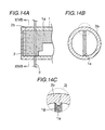
- Fig. 14A is a partial, vertical sectional view of a modification of the polarized wave separator according to the eleventh embodiment.
- Fig. 14B is a partial, sectional view taken along a line XIVB-XIVB of Fig. 14A.
- Fig. 14C is a partial, enlarged sectional view of the polarized wave separator of Fig. 14A.
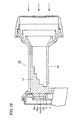
- Fig. 15 is a perspective view of a parabolic antenna provided with a polarized wave separator according to a twelfth embodiment of the present invention.
- Fig. 16 is a sectional view of the polarized wave separator according to the twelfth embodiment.
- Fig. 17A is a perspective view of an earthed cap for use in the polarized wave separator according to the twelfth embodiment.
- Fig. 17B is a sectional view taken along a line XVIIB-XVIIB of Fig. 17A.
- Fig. 17C is a sectional view illustrating a partition wall with the earthed cap of the twelfth embodiment being mounted in a slit.
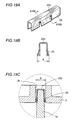
- Fig. 18A is a perspective view of an earthed cap for use in the polarized wave separator according to a first modification of the twelfth embodiment.
- Fig. 18B is a sectional view taken along a line XVIIIB-XVIIIB of Fig. 18A.
- Fig. 18C is a sectional view illustrating a partition wall with the earthed cap of the first modification being mounted in a slit.
- Fig. 19A is a perspective view of an earthed cap for use in the polarized wave separator according to a second modification of the twelfth embodiment.
- Fig. 19B is a sectional view taken along a line XIXB-XIXB of Fig. 19A.
- Fig. 19C is a sectional view illustrating a partition wall with the earthed cap of the second modification being mounted in a slit.
- Fig. 20A is a perspective view of an earthed cap for use in the polarized wave separator according to a third modification of the twelfth embodiment.
- Fig. 20B is a sectional view taken along a line XXB-XXB of Fig. 20A.
- Fig. 20C is a sectional view illustrating a partition wall with the earthed cap of the third modification being mounted in a slit.
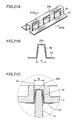
- Fig. 21A is a perspective view of an earthed cap for use in the polarized wave separator according to a fourth modification of the twelfth embodiment.
- Fig. 21B is a sectional view taken along a line XXIB-XXIB of Fig. 21A.
- Fig. 21C is a sectional view illustrating a partition wall with the earthed cap of the fourth modification being mounted in a slit.
- Fig. 22 is a graph for evaluation of wave losses in the polarized wave separator according to the fourth modification of the twelfth embodiment and in a conventional polarized wave separator.
- Fig. 23 illustrates how the wave loss is evaluated according to the twelfth embodiment.
- Fig. 24 is a perspective view of a conventional polarized wave separator before assembly.
- Fig. 25 is a partial, sectional view taken along a line XXV-XXV of Fig. 24.
- a polarized wave separator being used in a converter for receiving microwave according to the first embodiment will now be described.
- an opening portion 3a is formed in a substrate 3.
- a pair of wave receiving probes 4a, 4b is also formed on substrate 3, on opposite sides of opening portion 3a.
- the pair of wave receiving probes 4a, 4b is formed on a surface of substrate 3 facing a wave reflecting unit 2, as will be described later.
- Substrate 3 is, for example, a Teflon substrate or a glass epoxy substrate.
- a waveguide 1 is located on one side of substrate 3, and arranged so that one end of waveguide 1 encircles opening portion 3a as well as the pair of wave receiving probes 4a, 4b.
- Wave reflecting unit 2 is located on the other side of substrate 3, and arranged so that one end of a tubular portion 2b of wave reflecting unit 2 encircles opening portion 3a and the pair of wave receiving probes 4a, 4b.
- An end surface portion 2c is provided on the other end of tubular portion 2b.
- a wave reflecting surface 2a is formed on an inner side of end surface portion 2c, opposite to the pair of wave receiving probes 4a, 4b.
- an earthed surface (pattern) 5 is formed along the end surface of tubular portion 2b such that they contact with each other.
- an earthed surface is formed on the other surface of substrate 3 facing waveguide 1, along the end surface of waveguide 1. The earthed surface and the end surface of waveguide 1 are arranged to contact with each other.
- a partition wall la in a stepped form is provided within waveguide 1.
- Partition wall la extends through opening portion 3a to reach end surface portion 2c.
- An end portion of partition wall la facing wave reflecting surface 2a partitions the wave reflecting surface 2a into two portions.
- Partition wall la and waveguide 1 are formed in an integrated form by, e.g., aluminum die-casting.
- a wave-guiding space formed by waveguide 1, substrate 3 and tubular portion 2b is partitioned by partition wall 1a into two spaces.
- One wave-guiding space has one of the pair of wave receiving probes 4a, 4b located therein, and the other wave-guiding space has the other of the pair of wave receiving probes 4a, 4b located therein.
- the circularly polarized wave introduced into waveguide 1 is transformed to linearly polarized wave by means of partition wall la of the stepped shape.
- the circularly polarized wave includes clockwise polarized wave and counterclockwise polarized wave
- the transformed, linearly polarized wave includes a component transformed from the clockwise polarized wave and a component transformed from the counterclockwise polarized wave.
- one wave-guiding space (wave-guiding space A) catches the component of linearly polarized wave (component A) that was transformed from the clockwise polarized wave
- the other wave-guiding space (wave-guiding space B) catches the component of linearly polarized wave (component B) that was transformed from the counterclockwise polarized wave.
- component A travels through opening portion 3a to reach wave reflecting surface 2a, where it is reflected by wave reflecting surface 2a and received at one of the pair of wave receiving probes 4a, 4b. Similarly, component B is received at the other probe.
- Respective components A, B of the linearly polarized wave received at the pair of wave receiving probes 4a, 4b are input into a prescribed circuit (not shown) of the converter.
- the above-described polarized wave separator includes substrate 3 having opening portion 3a, and partition wall 1a extends through opening portion 3a to reach end surface portion 2c. Accordingly, the disadvantage of the prior art that poor contact between respective partition walls and the substrate results in escape of the separated wave from one wave-guiding space to the other is prevented, thereby improving polarized wave-separating characteristics.
- substrate 3 is contacted only by opposing tubular portion 2 of wave reflecting unit 2 and waveguide 1, and wave reflecting unit 2 and waveguide 1 are both ensured to attain better contact with surface 3.
- the wave is prevented from escaping outside waveguide 1 or wave reflecting unit 2.
- a polarized wave separator according to the second embodiment will now be described with reference to Figs. 3A, 3B and 3C. Specifically, an end portion 1b of partition wall 1a facing wave reflecting surface 2a is in a convex shape, and the narrowed portion contacts wave reflecting surface 2a. Otherwise, the configuration of the polarized wave separator according to the present embodiment is identical to that of the first embodiment shown in Figs. 1 and 2, and therefore, same members are denoted by same reference characters and description thereof is not repeated.
- polarized wave separator of the present embodiment contact of the convex end portion 1b of partition wall 1a with wave reflecting surface 2a ensures conduction between partition wall 1a and wave reflecting unit 2.
- loss of the separated wave is reduced, and escape of the components of the linearly polarized wave from one wave-guiding space A or B to the other wave-guiding space B or A is also restricted.
- polarized wave-separating characteristics for microwave are improved.
- a groove 2d is formed on the inner side of the end surface portion 2c of wave reflecting unit 2. This groove 2d accepts the end portion of partition wall la facing wave reflecting surface 2a. Otherwise, the configuration of the polarized wave separator according to the present embodiment is identical to that of the first embodiment shown in Figs. 1 and 2, and therefore, same members are denoted by same reference characters and detailed description thereof is not repeated.
- the end portion of partition wall la is received at groove 2d formed on end surface portion 2c, thereby ensuring separation between wave-guiding space A and wave-guiding space B.
- the components of the transformed, linearly polarized wave are prevented from escaping from one wave-guiding space A or B to the other wave-guiding space B or A.
- the polarized wave-separating characteristics for microwave are further improved.
- a groove 2e is formed on the inner side of end surface portion 2c of wave reflecting unit 2. This groove 2e receives an end portion 1c of partition wall 1a facing wave reflecting surface 2a. End portion 1c has an irregular shape in a saw-tooth waveform. Groove 2e has an irregular shape in a saw-tooth waveform corresponding to the form of end portion 1c. Otherwise, the configuration of the polarized wave separator according to the present embodiment is identical to that of the first embodiment shown in Figs. 1 and 2, so that same members are denoted by same reference characters and detailed description thereof is not repeated.
- the irregular shape in the saw-tooth waveform of end portion 1c of partition wall 1a matches the irregular shape in the saw-tooth waveform of groove 2e of end surface portion 2c.
- contact, and hence conduction, between partition wall 1a and wave reflecting unit 2 is ensured.
- loss of the separated wave is reduced, wave-guiding spaces A and B are reliably separated from each other, so that escape of components of the transformed, linearly polarized wave from one wave-guiding space A or B to the other is prevented.
- the polarized wave-separating characteristics for microwave are still further improved.
- end portion lc having the irregular shape in the saw-tooth waveform can be replaced by an end portion 1d having an irregular shape in a waveform, and groove 2e can be shaped corresponding to the waveform. Even in such a case, the same effects as in the case with the saw-tooth waveform can be obtained.
- end surface portion 2c of wave reflecting unit 2 is provided with a slit 2g penetrating therethrough.
- the end portion of partition wall 1a facing wave reflecting surface 2a is inserted into slit 2g, and riveted at the outside of end surface portion 2c, so that a riveted portion 1e is provided.
- the configuration of the polarized wave separator of the present embodiment is identical to that of the first embodiment shown in Figs. 1 and 2, and therefore, same members are denoted by same reference characters and description thereof is not repeated.
- the end portion of partition wall 1a is inserted into slit 2g, and riveted at the outside of end surface portion 2c to provide riveted portion le. Therefore, contact between partition wall la and wave reflecting unit 2 is ensured, providing good conduction therebetween. Correspondingly, loss of the separated wave is reduced, separation between wave-guiding spaces A and B is ensured, and escape of components of the transformed, linearly polarized wave from one wave-guiding space A or B to the other wave-guiding space B or A is prevented. As a result, the polarized wave-separating characteristics for microwave are further improved.
- Riveted portion le can be readily formed by inserting the end portion of partition wall la into slit 2g and riveting the portion protruding from end surface portion 2c, as shown in Fig. 6C.
- a slit 2g is formed which penetrates end surface portion 2c of wave reflecting unit 2.
- An end portion 1b of partition wall 1a facing wave reflecting surface 2a is inserted into slit 2g and is exposed from end surface portion 2c.
- a tapped hole 8 is provided at a portion of tubular portion 2b of wave reflecting unit 2 in contact with partition wall 1a, along a direction in which partition wall 1a extends, and a screw 7 is provided in tapped hole 8.
- a screw head 7a of screw 7 contacts end portion lb of partition wall 1a.
- the configuration of the polarized wave separator of the present embodiment is similar to that of the first embodiment shown in Figs. 1 and 2, and therefore, same members are denoted by same reference characters and description thereof is not repeated.
- end portion 1b of partition wall 1a is exposed outside the end surface portion 2c of wave reflecting unit 2, and screw head 7a of screw 7 attached to wave reflecting unit 2 contacts the exposed end portion 1b.
- connection between partition wall 1a and wave reflecting unit 2 is ensured, providing good conduction therebetween.
- loss of the separated wave is reduced, separation of wave-guiding spaces A and B is assured, so that components of the transformed, linearly polarized wave are prevented from escaping from wave-guiding space A to wave-guiding space B or vice versa.
- the polarized wave-separating characteristics for microwave are further improved.
- the use of the screw ensures conduction between partition wall 1a and wave reflecting unit 2, while preventing variation in dimension of parts or variation in assembling work.
- a groove 2d is formed on end surface portion 2c of wave reflecting unit 2 for receiving end portion 1b of partition wall 1a facing wave reflecting surface 2a. End portion 1b of partition wall 1a is inserted into groove 2d.
- a tapped hole 10 is formed, in which a screw 9 is provided. A tip portion of screw 9 contacts end portion lb of partition wall 1a.
- the configuration of the polarized wave separator of the present embodiment is similar to that of the first embodiment shown in Figs. 1 and 2, and therefore, same members are denoted by same reference characters and description thereof is not repeated.
- the tip portion of screw 9 attached to end surface portion 2c of wave reflecting unit 2 contacts end portion 1b of partition wall 1a.
- connection and hence good conduction between partition wall 1a and wave reflecting unit 2 are ensured.
- loss of the separated wave is reduced, wave-guiding spaces A and B are separated more reliably, so that escape of components of the transformed, linearly polarized wave from wave-guide space A to wave-guide space B, or vice versa, is prevented.
- the polarized wave-separating characteristics for microwave are further improved.
- a slit 2g is formed on end surface portion 2c of wave reflecting unit 2.
- An end portion of partition wall la facing wave reflecting surface 2a is inserted into slit 2g.
- a spring 11 which is formed of sheet metal.
- Spring 11 is preferably in a plate shape formed of sheet metal of aluminum, tin, phosphor bronze or the like.
- spring member 11 is provided between partition wall 1a and slit 2g in wave reflecting unit 2.
- resilience of the spring member 11 ensures contact of partition wall la and wave reflecting unit 2, providing good conduction therebetween.
- loss of the separated wave is reduced, and separation between wave-guiding spaces A and B is further ensured, thereby preventing escape of components of the transformed, linearly polarized wave from one wave-guiding space A or B to the other wave-guiding space B or A.
- the polarized wave-separating characteristics for microwave are further improved.
- a slit 2g is formed on end surface portion 2c of wave reflecting unit 2 for receiving end portion 1b of partition 1a facing wave reflecting surface 2a.
- End portion 1b of partition wall 1a is inserted into this slit 2g, and is exposed at the outside of end surface portion 2c.
- the exposed end portion 1b of partition wall 1a and end surface portion 2c of wave reflecting unit 2 surrounding the exposed end portion 1b are continuously covered by a conductive film 12.
- the configuration of the polarized wave separator of the present embodiment is similar to that of the first embodiment shown in Figs. 1 and 2, and thus, same members are denoted by same reference characters and description thereof is not repeated.
- the exposed end portion 1b of partition wall 1a and neighboring end surface portion 2c of wave reflecting unit 2 are continuously covered by conductive film 12.
- partition wall 1a and wave reflecting unit 2 are reliably contacted with each other via conductive film 12, thereby ensuring good conduction therebetween.
- loss of the separated wave is reduced, and wave-guiding spaces A and B are separated from each other more reliably, so that components of the transformed, linearly polarized wave are prevented from escaping from one wave-guiding space A or B to the other wave-guiding space B or A.
- the polarized wave-separating characteristics for microwave are further improved.
- metal foil with an adhesive applied thereon for example, may be employed to attain the same effects.
- conductive paste or conductive glue 13 may be applied instead of conductive film 12 or metal foil. In this case, again, the same effects can be obtained.
- a slit 2g is formed at end surface portion 2c of wave reflecting unit 2, and end portion 1b of partition wall 1a facing wave reflecting surface 2a is inserted into slit 2g.
- End portion 1b of partition wall 1a and end surface portion 2c surrounding the exposed end portion 1b are welded by ultrasonic welding or laser welding, so that a welded portion 14 is formed.
- Welded portion 14 is formed, as shown in Fig. 12C, by welding a portion of end portion 1b of partition 1a that was extended through slit 2g and protruded from end surface portion 2c to a portion of end surface portion 2c of wave reflecting unit 2 surrounding the protruded portion of end portion 1b.
- ultrasonic welding or laser welding is employed.
- the configuration of the polarized wave separator of the present embodiment is similar to that of the first embodiment as shown in Figs. 1 and 2, and therefore, same members are denoted by same reference characters and description thereof is not repeated.
- welded portion 14 is formed by welding end portion 1b of partition wall 1a and end surface portion 2c of wave reflecting unit 2 surrounding the protruded end portion 1b.
- partition wall 1a and wave reflecting unit 2 are reliably contacted, providing good conduction therebetween.
- loss of the separated wave is reduced, and separation between wave-guiding spaces A and B is ensured, so that components of the transformed, linearly polarized wave are prevented from escaping from wave-guiding space A to wave-guiding space B or vice versa.
- the polarized wave-separating characteristics for microwave are further improved.
- a convex portion 1f is formed at a portion of partition wall 1a contacting tubular portion 2b of wave reflecting unit 2, along a direction in which partition wall 1a extends.
- a concave portion 2h is formed on the inner side of tubular portion 2b, so that the convex portion 1f of partition wall 1a is fitted into the concave portion 2h.
- any of the structures described in the first through tenth embodiments is employed.
- fitting of convex portion 1f of partition wall 1a into concave portion 2h of tubular portion 2b further ensures separation between wave-guiding spaces A and B.
- escape of components of the transformed, linearly polarized wave from one wave-guiding space A or B to the other wave-guiding space B or A is prevented more reliably.
- the polarized wave-separating characteristics for microwave are still further improved.
- partition wall 1a is provided with convex portion 1f and tubular portion 2b is provided with concave portion 2h in this embodiment, it is also possible to provide partition wall la with a concave portion lg and tubular portion 2b with a convex portion 2j, as shown in Figs. 14A, 14B and 14C. In this case, again, the same effects can be obtained.
- the internal diameters of waveguide 1 and tubular portion 2 are made substantially the same as the opening diameter of opening portion 3a.
- the opening diameter of opening portion 3a can be made smaller than the internal diameters of waveguide 1 and tubular portion 2, for example. The same effects can be obtained as long as the internal circumferences of waveguide 1 and tubular portion 2 encircle the opening portion 3a successfully.
- a polarized wave separator according to the twelfth embodiment of the present invention will now be described.
- the radio wave sent from a satellite is reflected and integrated by parabolic antenna 21, and received at a satellite broadcasting receiving converter body (hereinafter, simply referred to as "converter body") 22 that includes the polarized wave separator.
- the wave received at converter body 22 is sent via a cable 23 to domestic appliances (not shown).
- converter body 22 includes a chassis with waveguide 24 having a partition wall la provided therein, and an electrically short-circuited plate (hereinafter, "short plate") 2 as a wave reflecting unit having a wave reflecting surface 2a provided therein.
- Partition wall la extends through an opening portion 3a provided at a substrate portion 3 to reach short plate 2.
- the end portion of partition wall la is received at a slit portion 2k formed on short plate 2.
- the short plate refers to a member that is electrically short-circuited with the waveguide for reflecting the radio wave coming into the waveguide to the opposite direction.
- a conductive-type earthed cap 25a is mounted between the end portion of partition wall 1a and slit portion 2k.
- Earthed cap 25a is configured to cover the end portion of partition wall 1a, and its side portion formed towards a direction in which partition wall 1a extends is provided with a cut and bent portion 26 which is cut and bent outwards.
- a width A of earthed cap 25a including the cut and bent portion 26 is set slightly greater than a spacing B of slit 2k.
- the earthed cap 25b according to the first modification has a portion 26 that is cut and bent inwards, specifically on its side portion formed towards the direction in which partition wall 1a extends.
- the width A of earthed cap 25b is set slightly greater than the width B of slit 2k, as shown in Figs. 18B and 18C.
- earthed cap 25b is mounted on the end portion of partition wall 1a before being inserted into slit 2k formed in short plate 2, efficiency of the assembling work improves. In addition, it is readily possible to confirm accurate positioning of earthed cap 25b upon assembling.
- the earthed cap 25c according to the second modification has a portion 26 that is cut and bent outwards, specifically on its side portion formed towards the direction in which partition wall 1a extends.
- the width A of earthed cap 25c including cut and bent portion 26 is set slightly greater than the width B of slit 2k, as shown in Figs. 19B and 19C.
- earthed cap 25c again, when the end portion of partition wall 1a is mounted in slit 2k, earthed cap 25c is prevented from falling off, and electrical conduction between short plate 2 and partition wall la is ensured as the cut and bent portion 26 contacts short pate 2.
- earthed cap 25c can be mounted on the end portion of partition wall 1a before insertion into slit 2k formed in short plate 2. This improves efficiency of the assembling work, and simplifies confirmation of accurate positioning of earthed cap 25c when assembling.
- earthed cap 25c according to the second modification can be manufactured at a lower cost than earthed cap 25a of the twelfth embodiment described first, since cut and bent portion 26 is made by cutting the side portion simply from its open end.
- the earthed cap 25d according to the third modification has a hooked portion 27 which is formed such that it closely contacts wave reflecting surface 2a of short plate 2 face to face.
- the width A of earthed cap 25d excluding hooked portion 27 is set slightly greater than the width B of slit 2k.
- Earthed cap 25d is first mounted in slit 2k, and then the end portion of partition wall 1a is inserted into the earthed cap 2d mounted in slit 2k. At this time, as width A is made slightly greater than width B, the partition wall and the short plate are fitted reliably, preventing displacement therebetween. Electrical conduction between short plate 2 and partition wall 1a is also ensured.
- earthed cap 25d is prevented from moving or falling off upon or after assembling.
- the earthed cap 25e according to the fourth modification has a hooked portion 27 formed such that it closely contacts wave reflecting surface 2a of short plate 2 face to face. It also has, on its side portion, a portion 26 cut and bent inwards.
- the width A of earthed cap 25e excluding hooked portion 27 is set slightly greater than the width B of slit 2k.
- earthed cap 25e of the fourth modification further ensures electrical conduction between short plate 2 and partition wall la because of the provision of cut and bent portion 26.
- wave loss of the polarized wave separator provided with earthed cap 25e of the fourth modification was evaluated using a network analyzer 34 as shown in Fig. 23.
- a waveguide 31 was attached to the wave incoming side of converter body 22, and an input signal was applied via a coaxial line 32 into waveguide 31.
- a passing signal traveling through waveguide 31 to converter body 22 and received at wave receiving probes 4a, 4b was detected by network analyzer 34.
- Fig. 22 shows the evaluation result. As shown in Fig. 22, it was found that the wave loss by the polarized wave separator according to the present invention (expressed with ⁇ ) was reduced compared to that of a conventional polarized wave separator ( ⁇ ).
Landscapes
- Aerials With Secondary Devices (AREA)
- Waveguide Switches, Polarizers, And Phase Shifters (AREA)
Abstract
Description
- The present invention relates to polarized wave separators, and more particularly to a polarized wave separator for use in a receiving converter (a low noise blockdown converter, LNB) that receives radio wave from a broadcasting or communication satellite.
- Microwave being used in satellite broadcasting normally consists of two components. As typical microwave, circularly polarized wave includes clockwise polarized wave and counterclockwise polarized wave. Linearly polarized wave includes vertically polarized wave and horizontally polarized wave.
- The receiving converter is required to efficiently separate such two components from each other, and a polarized wave separator is used for such separation of microwave. As a representative of conventional polarized wave separators for use in the receiving converters, a polarized wave separator for separating the components included in circularly polarized wave will now be described.
- Referring to Figs. 24 and 25, a pair of
wave receiving probes substrate 103. Awaveguide 101 is placed on one side ofsubstrate 103. A waveguide partition wall lOla in a stepped shape is formed withinwaveguide 101, which partitions the interior ofwaveguide 101 into two portions. - A
wave reflecting unit 102 is placed on the other side ofsubstrate 103. A wave reflectingunit partition wall 102a is formed withinwave reflecting unit 102, which partitions the interior thereof into two portions. Awave reflecting surface 102b is formed on an end surface ofwave reflecting unit 102 opposite tosubstrate 103. - On a surface of
substrate 103 facingwave reflecting unit 102, an earthed surface (pattern) 105 is formed along end surfaces ofwave reflecting unit 102 and itspartition wall 102a such that they contact with each other. On the other surface ofsubstrate 103 facingwaveguide 101, another earthed surface (not shown) is formed along end surfaces ofwaveguide 101 and its partition wall lOla such that they contact with each other. - The
earthed surface 105 for contact withwave reflecting unit 102 and the earthed surface for contact withwaveguide 101 are electrically connected to each other via a throughhole 106. Thus,waveguide 101 andwave reflecting unit 102 are both maintained at an earth potential viasubstrate 103. - The pair of
wave receiving probes substrate 103 on its side facingwave reflecting unit 102. Interconnection portions ofwave receiving probes earthed surface 105,wave receiving unit 102 andwaveguide 101. - Waveguide partition wall lOla and wave reflecting
unit partition wall 102a act to partition the interior ofwaveguide 101 andwave reflecting unit 102, respectively, into two wave-guiding spaces. Circularly polarized wave caught withinwaveguide 101 is separated bywaveguide partition wall 101a and introduced into respective wave-guiding spaces. - The conventional polarized wave separators have configurations as described above.
- With such a conventional polarized wave separator, however, there exist several problems conceivable as follows. To prevent the wave within
waveguide 101 andwave reflecting unit 102 from externally escaping, or to reduce noise, it is necessary to ensure that respective end surfaces of partition walls lOla, 102a,waveguide 101 andwave reflecting unit 102 contact their corresponding earthed surfaces. - If the secure contact between wave reflecting
unit partition wall 102a andearthed surface 105 onsubstrate 103 is ensured, however, good contact between the end surface ofwaveguide 101 and the corresponding earthed surface may not be achieved. - As a result, the wave may escape
fiom waveguide 101, or the wave may not be separated successfully. - In addition, since
wave reflecting unit 102 andwaveguide 101 are electrically connected to each other viasubstrate 103, there may arise a problem that the wave introduced intowaveguide 101 will be attenuated bysubstrate 103 before reachingwave reflecting surface 102b, which results in further weakening of the wave. Hereinafter, such reduction in strength of the wave due to escape and/or attenuation will be referred to as "wave loss". - The present invention is directed to solve the conceivable problems as described above. An object of the present invention is to provide a polarized wave separator that ensures separation of radio wave while suppressing escape of the wave, thereby reducing the wave loss.
- A polarized wave separator according to the present invention includes a substrate portion, a pair of wave receiving portions, a waveguide, and a wave reflecting unit. The substrate has an opening portion. The pair of wave receiving portions is formed on the substrate on opposite sides in a radial direction of the opening portion. The waveguide is located on one side of the substrate portion, and has a partition wall portion provided therein. The wave reflecting unit is located on the other side of the substrate portion, and has a wave reflecting surface formed on its inner side. The waveguide, substrate portion and wave reflecting unit together form a wave-guiding space. The partition wall portion extends through the opening portion to the wave reflecting unit, and divides the wave reflecting surface into two portions. By the partition wall, the wave-guiding space is partitioned into two spaces, one in which one of the pair of wave receiving portions is located and the other in which the other of the pair of wave receiving portions is located.
- According to this polarized wave separator, compared to the case of a conventional polarized wave separator in which the waveguide and the wave reflecting unit are located on respective sides of the substrate portion with no opening therein, the wave-guiding space formed by the waveguide, substrate and wave reflecting unit is partitioned by the single partition wall penetrating the opening formed on the substrate. Therefore, the separated wave caught in the respective wave-guiding spaces is prevented from escaping from one wave-guiding space to the other wave-guiding space both in the waveguide and in the wave reflecting unit near the substrate portion. This improves polarized wave-separating characteristics. In addition, the wave guided in the wave-guiding spaces is propagated to the wave reflecting surface without being interrupted by the substrate portion. This reduces the wave loss. Furthermore, the substrate portion is contacted only by the tubular portion of the wave reflecting unit and the waveguide, so that they both can make good contact with the substrate. Thus, it is possible to prevent the separated wave from escaping outside the waveguide or the tubular portion, so that the wave loss can be reduced.
- Preferably, the waveguide is located such that the internal circumference of the waveguide encircles the opening portion. The wave reflecting unit includes the tubular portion that is located on the other side of the substrate portion from the waveguide, and an end surface portion that is located on an end of the tubular portion where a wave reflecting surface is formed. The partition wall portion contacts at least the end surface portion, so that it is electrically connected with the wave reflecting unit.
- With such a configuration, conduction between the partition wall portion and the wave reflecting unit is ensured, so that the loss of the separated wave is alleviated. Further, it is possible to prevent escape of the separated wave from one wave-guiding space to the other wave-guiding space at least through a gap between the partition wall portion and the end surface portion, so that the separating characteristics are further improved.
- To ensure that the partition wall portion and the wave reflecting unit are electrically connected in a good condition and the wave is prevented from escaping as described above, the following configurations are desirable.
- The end portion of the partition portion facing the wave reflecting surface is preferably in a convex shape, and this convex shaped end portion contacts the wave reflecting surface.
- Preferably, a groove portion is formed on an inner side of the end surface portion of the wave reflecting unit, so that the end portion of the partition wall portion facing the wave reflecting surface is accepted in the groove portion. In particular, it is desired that the end portion of the partition wall portion is in a saw-tooth waveform or a waveform, and the groove portion is formed in a shape corresponding thereto. This assures the contact between the partition wall portion and the wave reflecting unit.
- Still preferably, the end surface portion of the wave reflecting unit is provided with a female screw portion and a male screw portion mounted onto the female screw portion, and the male screw portion contacts the partition wall portion.
- Preferably, a slit portion is formed on the end surface portion which penetrates the end surface portion, and the end portion of the partition wall portion facing the wave reflecting surface is inserted into the slit portion.
- Still preferably, the end portion of the partition wall portion penetrates the slit portion and is riveted at the outside of the end surface portion.
- Preferably, a conductive member is mounted between the end portion of the partition wall portion and the slit portion. The conductive member preferably includes an elastic body or a resin.
- Still preferably, the end portion of the partition wall portion penetrates the slit portion and is exposed at the end surface portion, and a conductive member is formed to directly cover the end surface portion and the exposed end portion. The conductive member preferably includes a conductive film, metal foil, conductive paste or conductive adhesive.
- Preferably, the end portion of the partition wall portion penetrates the slit portion and is exposed at the end surface portion, and the end surface portion and the exposed end portion are welded.
- Still preferably, the partition wall portion contacts the tubular portion, and at the portion where the tubular portion and the partition wall portion contact with each other, a concave portion is provided to either one of the tubular portion and the partition wall portion that is formed along a direction in which the partition wall portion extends, and a convex portion is provided to the other of the tubular portion and the partition wall portion that is fitted into the concave portion.
- Preferably, a conductive, earthed cap portion is provided between the partition wall portion and the slit portion to cover the end portion.
- In this case, provision of such earthed cap portion ensures that the partition wall portion and the end portion are electrically conducted to each other.
- Preferably, the earthed cap portion includes a side portion that is formed towards a direction in which the partition wall portion extends, and a cut and bent portion that is bent towards the slit portion side or towards the partition wall portion side.
- In this case, the cut and bent portion further ensures the electrical conduction between the partition wall portion and the end surface portion, and also prevents the earthed cap portion from falling off.
- Still preferably, the earthed cap portion includes a hooked portion that closely contacts the wave reflecting surface of the end surface portion.
- In this case, by the hooked portion in close contact with the wave reflecting surface, the earthed cap portion is secured on the wave reflecting surface, so that it is reliably mounted in the slit portion.
- The foregoing and other objects, features, aspects and advantages of the present invention will become more apparent from the following detailed description of the present invention when taken in conjunction with the accompanying drawings.
- Fig. 1 is a perspective view of a polarized wave separator before assembly according to a first embodiment of the present invention.
- Fig. 2 is a cross sectional view taken along a line II-II of Fig. 1.
- Fig. 3A is a partial, vertical sectional view of a polarized wave separator according to a second embodiment of the present invention.
- Fig. 3B is a partial, enlarged sectional view of the polarized wave separator of Fig. 3A.
- Fig. 3C is a side view of the polarized wave separator of Fig. 3A.
- Fig. 4A is a partial, vertical sectional view of a polarized wave separator according to a third embodiment of the present invention.
- Fig. 4B is a partial, enlarged sectional view of the polarized wave separator of Fig. 4A.
- Fig. 4C is a side view of the polarized wave separator of Fig. 4A.
- Fig. 5A is a partial, vertical sectional view of a polarized wave separator according to a fourth embodiment of the present invention.
- Fig. 5B is a partial, sectional view taken along a line VB-VB of Fig. 5A.
- Fig. 5C is a partial, enlarged sectional view of the polarized wave separator of Fig. 5A.
- Fig. 5D is a partial, enlarged sectional view of a modification of the polarized wave separator of Fig. 5A.
- Fig. 6A is a partial, vertical sectional view of a polarized wave separator according to a fifth embodiment of the present invention.
- Fig. 6B is a partial, enlarged sectional view of the polarized wave separator of Fig. 6A.
- Fig. 6C is a partial, vertical sectional view of the polarized wave separator of Fig. 6A before formation of a riveted portion.
- Fig. 7A is a partial, vertical sectional view of a polarized wave separator according to a sixth embodiment of the present invention.
- Fig. 7B is a partial, sectional view taken along a line VIIB-VIIB of Fig. 7A.
- Fig. 7C is a partial, enlarged sectional view of the polarized wave separator of Fig. 7A.
- Fig. 8A is a partial, vertical sectional view of a polarized wave separator according to a seventh embodiment of the present invention.
- Fig. 8B is a partial, sectional view taken along a line VIIIB-VIIIB of Fig. 8A.
- Fig. 8C is a partial, enlarged sectional view of the polarized wave separator of Fig. 8A.
- Fig. 9A is a partial, vertical sectional view of a polarized wave separator according to an eighth embodiment of the present invention.
- Fig. 9B is a partial, enlarged sectional view of the polarized wave separator of Fig. 9A.
- Fig. 9C is a side view of the polarized wave separator of Fig. 9A.
- Fig. 10A is a partial, vertical sectional view of a polarized wave separator according to a ninth embodiment of the present invention.
- Fig. 10B is a partial, enlarged sectional view of the polarized wave separator of Fig. 10A.
- Fig. 10C is a side view of the polarized wave separator of Fig. 10A.
- Fig. 11A is a partial, vertical sectional view of a modification of the polarized wave separator according to the ninth embodiment.
- Fig. 11B is a partial, enlarged sectional view of the polarized wave separator of Fig. 11A.
- Fig. 11C is a side view of the polarized wave separator of Fig. 11A.
- Fig. 12A is a partial, vertical sectional view of a polarized wave separator according to a tenth embodiment of the present invention.
- Fig. 12B is a partial, enlarged sectional view of the polarized wave separator of Fig. 12A.
- Fig. 12C is a partial, vertical sectional view of the polarized wave separator of Fig. 12A before formation of a welded portion.
- Fig. 13A is a partial, vertical sectional view of a polarized wave separator according to an eleventh embodiment of the present invention.
- Fig. 13B is a partial, sectional view taken along a line XIIIB-XIIIB of Fig. 13A.
- Fig. 13C is a partial, enlarged sectional view of the polarized wave separator of Fig. 13A.
- Fig. 14A is a partial, vertical sectional view of a modification of the polarized wave separator according to the eleventh embodiment.
- Fig. 14B is a partial, sectional view taken along a line XIVB-XIVB of Fig. 14A.
- Fig. 14C is a partial, enlarged sectional view of the polarized wave separator of Fig. 14A.
- Fig. 15 is a perspective view of a parabolic antenna provided with a polarized wave separator according to a twelfth embodiment of the present invention.
- Fig. 16 is a sectional view of the polarized wave separator according to the twelfth embodiment.
- Fig. 17A is a perspective view of an earthed cap for use in the polarized wave separator according to the twelfth embodiment.
- Fig. 17B is a sectional view taken along a line XVIIB-XVIIB of Fig. 17A.
- Fig. 17C is a sectional view illustrating a partition wall with the earthed cap of the twelfth embodiment being mounted in a slit.
- Fig. 18A is a perspective view of an earthed cap for use in the polarized wave separator according to a first modification of the twelfth embodiment.
- Fig. 18B is a sectional view taken along a line XVIIIB-XVIIIB of Fig. 18A.
- Fig. 18C is a sectional view illustrating a partition wall with the earthed cap of the first modification being mounted in a slit.
- Fig. 19A is a perspective view of an earthed cap for use in the polarized wave separator according to a second modification of the twelfth embodiment.
- Fig. 19B is a sectional view taken along a line XIXB-XIXB of Fig. 19A.
- Fig. 19C is a sectional view illustrating a partition wall with the earthed cap of the second modification being mounted in a slit.
- Fig. 20A is a perspective view of an earthed cap for use in the polarized wave separator according to a third modification of the twelfth embodiment.
- Fig. 20B is a sectional view taken along a line XXB-XXB of Fig. 20A.
- Fig. 20C is a sectional view illustrating a partition wall with the earthed cap of the third modification being mounted in a slit.
- Fig. 21A is a perspective view of an earthed cap for use in the polarized wave separator according to a fourth modification of the twelfth embodiment.
- Fig. 21B is a sectional view taken along a line XXIB-XXIB of Fig. 21A.
- Fig. 21C is a sectional view illustrating a partition wall with the earthed cap of the fourth modification being mounted in a slit.
- Fig. 22 is a graph for evaluation of wave losses in the polarized wave separator according to the fourth modification of the twelfth embodiment and in a conventional polarized wave separator.
- Fig. 23 illustrates how the wave loss is evaluated according to the twelfth embodiment.
- Fig. 24 is a perspective view of a conventional polarized wave separator before assembly.
- Fig. 25 is a partial, sectional view taken along a line XXV-XXV of Fig. 24.
- A polarized wave separator being used in a converter for receiving microwave according to the first embodiment will now be described.
- Referring to Figs. 1 and 2, an
opening portion 3a is formed in asubstrate 3. A pair ofwave receiving probes substrate 3, on opposite sides of openingportion 3a. The pair ofwave receiving probes substrate 3 facing awave reflecting unit 2, as will be described later.Substrate 3 is, for example, a Teflon substrate or a glass epoxy substrate. - A
waveguide 1 is located on one side ofsubstrate 3, and arranged so that one end ofwaveguide 1encircles opening portion 3a as well as the pair ofwave receiving probes - Wave reflecting
unit 2 is located on the other side ofsubstrate 3, and arranged so that one end of atubular portion 2b ofwave reflecting unit 2 encircles openingportion 3a and the pair ofwave receiving probes end surface portion 2c is provided on the other end oftubular portion 2b. Awave reflecting surface 2a is formed on an inner side ofend surface portion 2c, opposite to the pair ofwave receiving probes - On a surface of
substrate 3 facingwave reflecting unit 2, an earthed surface (pattern) 5 is formed along the end surface oftubular portion 2b such that they contact with each other. Similarly, an earthed surface (not shown) is formed on the other surface ofsubstrate 3 facingwaveguide 1, along the end surface ofwaveguide 1. The earthed surface and the end surface ofwaveguide 1 are arranged to contact with each other. -
Earthed surface 5 in contact withtubular portion 2b ofwave reflecting unit 2 and the earthed surface in contact withwaveguide 1 are electrically connected to each other via a throughhole 6. Thus,waveguide 1 andwave reflecting unit 2 are both held at an earth potential viasubstrate 3. Interconnection portions ofwave receiving probes substrate 3 are electrically isolated fromwave reflecting unit 2 andwaveguide 1. - A partition wall la in a stepped form is provided within
waveguide 1. Partition wall la extends through openingportion 3a to reachend surface portion 2c. An end portion of partition wall la facingwave reflecting surface 2a partitions thewave reflecting surface 2a into two portions. Partition wall la andwaveguide 1 are formed in an integrated form by, e.g., aluminum die-casting. - A wave-guiding space formed by
waveguide 1,substrate 3 andtubular portion 2b is partitioned bypartition wall 1a into two spaces. One wave-guiding space has one of the pair ofwave receiving probes wave receiving probes - An operation of the polarized wave separator described above will now be explained.
- In the case where microwave is circularly polarized wave, the circularly polarized wave introduced into
waveguide 1 is transformed to linearly polarized wave by means of partition wall la of the stepped shape. As the circularly polarized wave includes clockwise polarized wave and counterclockwise polarized wave, the transformed, linearly polarized wave includes a component transformed from the clockwise polarized wave and a component transformed from the counterclockwise polarized wave. - Of the two wave-guiding spaces partitioned by
partition wall 1a, one wave-guiding space (wave-guiding space A) catches the component of linearly polarized wave (component A) that was transformed from the clockwise polarized wave, and the other wave-guiding space (wave-guiding space B) catches the component of linearly polarized wave (component B) that was transformed from the counterclockwise polarized wave. - Thus separated component A travels through opening
portion 3a to reachwave reflecting surface 2a, where it is reflected bywave reflecting surface 2a and received at one of the pair ofwave receiving probes - Respective components A, B of the linearly polarized wave received at the pair of
wave receiving probes - As shown in Figs. 24 and 25, different from the case of the conventional polarized wave separator in which
partition walls substrate 103, the above-described polarized wave separator includessubstrate 3 havingopening portion 3a, andpartition wall 1a extends through openingportion 3a to reachend surface portion 2c. Accordingly, the disadvantage of the prior art that poor contact between respective partition walls and the substrate results in escape of the separated wave from one wave-guiding space to the other is prevented, thereby improving polarized wave-separating characteristics. - Further,
substrate 3 is contacted only by opposingtubular portion 2 ofwave reflecting unit 2 andwaveguide 1, andwave reflecting unit 2 andwaveguide 1 are both ensured to attain better contact withsurface 3. Thus, the wave is prevented from escaping outsidewaveguide 1 orwave reflecting unit 2. - Still further, two components A, B separated by
partition wall 1a are propagated to wave reflectingsurface 2a without being interrupted bysubstrate 3. Thus, the wave loss is reduced. - A polarized wave separator according to the second embodiment will now be described with reference to Figs. 3A, 3B and 3C. Specifically, an
end portion 1b ofpartition wall 1a facingwave reflecting surface 2a is in a convex shape, and the narrowed portion contacts wave reflectingsurface 2a. Otherwise, the configuration of the polarized wave separator according to the present embodiment is identical to that of the first embodiment shown in Figs. 1 and 2, and therefore, same members are denoted by same reference characters and description thereof is not repeated. - According to the polarized wave separator of the present embodiment, contact of the
convex end portion 1b ofpartition wall 1a withwave reflecting surface 2a ensures conduction betweenpartition wall 1a andwave reflecting unit 2. Thus, loss of the separated wave is reduced, and escape of the components of the linearly polarized wave from one wave-guiding space A or B to the other wave-guiding space B or A is also restricted. As a result, polarized wave-separating characteristics for microwave are improved. - A polarized wave separator according to the third embodiment will now be described. Referring to Figs. 4A, 4B and 4C, a
groove 2d is formed on the inner side of theend surface portion 2c ofwave reflecting unit 2. Thisgroove 2d accepts the end portion of partition wall la facingwave reflecting surface 2a. Otherwise, the configuration of the polarized wave separator according to the present embodiment is identical to that of the first embodiment shown in Figs. 1 and 2, and therefore, same members are denoted by same reference characters and detailed description thereof is not repeated. - According to the polarized wave separator of the present embodiment, the end portion of partition wall la is received at
groove 2d formed onend surface portion 2c, thereby ensuring separation between wave-guiding space A and wave-guiding space B. Thus, the components of the transformed, linearly polarized wave are prevented from escaping from one wave-guiding space A or B to the other wave-guiding space B or A. As a result, the polarized wave-separating characteristics for microwave are further improved. - A polarized wave separator according to the fourth embodiment will now be described. Referring to Figs. 5A, 5B and 5C, a
groove 2e is formed on the inner side ofend surface portion 2c ofwave reflecting unit 2. Thisgroove 2e receives anend portion 1c ofpartition wall 1a facingwave reflecting surface 2a.End portion 1c has an irregular shape in a saw-tooth waveform.Groove 2e has an irregular shape in a saw-tooth waveform corresponding to the form ofend portion 1c. Otherwise, the configuration of the polarized wave separator according to the present embodiment is identical to that of the first embodiment shown in Figs. 1 and 2, so that same members are denoted by same reference characters and detailed description thereof is not repeated. - According to the polarized wave separator of the present embodiment, the irregular shape in the saw-tooth waveform of
end portion 1c ofpartition wall 1a matches the irregular shape in the saw-tooth waveform ofgroove 2e ofend surface portion 2c. Thus, contact, and hence conduction, betweenpartition wall 1a andwave reflecting unit 2 is ensured. Correspondingly, loss of the separated wave is reduced, wave-guiding spaces A and B are reliably separated from each other, so that escape of components of the transformed, linearly polarized wave from one wave-guiding space A or B to the other is prevented. As a result, the polarized wave-separating characteristics for microwave are still further improved. - It is noted that, as shown in Fig. 5D, end portion lc having the irregular shape in the saw-tooth waveform can be replaced by an
end portion 1d having an irregular shape in a waveform, andgroove 2e can be shaped corresponding to the waveform. Even in such a case, the same effects as in the case with the saw-tooth waveform can be obtained. - A polarized wave separator according to the fifth embodiment will now be described. Referring to Figs. 6A and 6B,
end surface portion 2c ofwave reflecting unit 2 is provided with aslit 2g penetrating therethrough. The end portion ofpartition wall 1a facingwave reflecting surface 2a is inserted intoslit 2g, and riveted at the outside ofend surface portion 2c, so that a rivetedportion 1e is provided. Otherwise, the configuration of the polarized wave separator of the present embodiment is identical to that of the first embodiment shown in Figs. 1 and 2, and therefore, same members are denoted by same reference characters and description thereof is not repeated. - According to the polarized wave separator of the present embodiment, the end portion of
partition wall 1a is inserted intoslit 2g, and riveted at the outside ofend surface portion 2c to provide riveted portion le. Therefore, contact between partition wall la andwave reflecting unit 2 is ensured, providing good conduction therebetween. Correspondingly, loss of the separated wave is reduced, separation between wave-guiding spaces A and B is ensured, and escape of components of the transformed, linearly polarized wave from one wave-guiding space A or B to the other wave-guiding space B or A is prevented. As a result, the polarized wave-separating characteristics for microwave are further improved. - Riveted portion le can be readily formed by inserting the end portion of partition wall la into
slit 2g and riveting the portion protruding fromend surface portion 2c, as shown in Fig. 6C. - A polarized wave separator according to the sixth embodiment will now be described. Referring to Figs. 7A, 7B and 7C, a
slit 2g is formed which penetratesend surface portion 2c ofwave reflecting unit 2. Anend portion 1b ofpartition wall 1a facingwave reflecting surface 2a is inserted intoslit 2g and is exposed fromend surface portion 2c. In addition, at a portion oftubular portion 2b ofwave reflecting unit 2 in contact withpartition wall 1a, a tappedhole 8 is provided along a direction in whichpartition wall 1a extends, and ascrew 7 is provided in tappedhole 8. Ascrew head 7a ofscrew 7 contacts end portion lb ofpartition wall 1a. - Otherwise, the configuration of the polarized wave separator of the present embodiment is similar to that of the first embodiment shown in Figs. 1 and 2, and therefore, same members are denoted by same reference characters and description thereof is not repeated.
- According to the polarized wave separator of the present embodiment,
end portion 1b ofpartition wall 1a is exposed outside theend surface portion 2c ofwave reflecting unit 2, and screwhead 7a ofscrew 7 attached to wave reflectingunit 2 contacts the exposedend portion 1b. Thus, connection betweenpartition wall 1a andwave reflecting unit 2 is ensured, providing good conduction therebetween. Correspondingly, loss of the separated wave is reduced, separation of wave-guiding spaces A and B is assured, so that components of the transformed, linearly polarized wave are prevented from escaping from wave-guiding space A to wave-guiding space B or vice versa. As a result, the polarized wave-separating characteristics for microwave are further improved. - In addition, the use of the screw ensures conduction between
partition wall 1a andwave reflecting unit 2, while preventing variation in dimension of parts or variation in assembling work. - A polarized wave separator according to the seventh embodiment will now be described. Referring to Figs. 8A, 8B and 8C, a
groove 2d is formed onend surface portion 2c ofwave reflecting unit 2 for receivingend portion 1b ofpartition wall 1a facingwave reflecting surface 2a.End portion 1b ofpartition wall 1a is inserted intogroove 2d. On the outside ofend surface portion 2c ofwave reflecting unit 2, a tappedhole 10 is formed, in which ascrew 9 is provided. A tip portion ofscrew 9 contacts end portion lb ofpartition wall 1a. - Otherwise, the configuration of the polarized wave separator of the present embodiment is similar to that of the first embodiment shown in Figs. 1 and 2, and therefore, same members are denoted by same reference characters and description thereof is not repeated.
- According to the polarized wave separator of the present embodiment, the tip portion of
screw 9 attached to endsurface portion 2c ofwave reflecting unit 2 contacts endportion 1b ofpartition wall 1a. Thus, connection and hence good conduction betweenpartition wall 1a andwave reflecting unit 2 are ensured. Correspondingly, loss of the separated wave is reduced, wave-guiding spaces A and B are separated more reliably, so that escape of components of the transformed, linearly polarized wave from wave-guide space A to wave-guide space B, or vice versa, is prevented. As a result, the polarized wave-separating characteristics for microwave are further improved. - A polarized wave separator according to the eighth embodiment will now be described. Referring to Figs. 9A, 9B and 9C, a
slit 2g is formed onend surface portion 2c ofwave reflecting unit 2. An end portion of partition wall la facingwave reflecting surface 2a is inserted intoslit 2g. Provided between partition wall la and slit 2g is aspring 11, which is formed of sheet metal.Spring 11 is preferably in a plate shape formed of sheet metal of aluminum, tin, phosphor bronze or the like. - Otherwise, the configuration of the present embodiment is identical to that of the first embodiment shown in Figs. 1 and 2, and therefore, same members are denoted by same reference characters and description thereof is not repeated.
- According to the polarized wave separator of the present embodiment,
spring member 11 is provided betweenpartition wall 1a and slit 2g inwave reflecting unit 2. Thus, resilience of thespring member 11 ensures contact of partition wall la andwave reflecting unit 2, providing good conduction therebetween. Correspondingly, loss of the separated wave is reduced, and separation between wave-guiding spaces A and B is further ensured, thereby preventing escape of components of the transformed, linearly polarized wave from one wave-guiding space A or B to the other wave-guiding space B or A. As a result, the polarized wave-separating characteristics for microwave are further improved. - In addition, as the spring is easily mounted/dismounted, variation in assembling work is reduced, which helps improve the quality of the polarized wave separator. It is noted that, besides the plate spring as described above, any conductive member or resin having appropriate resilience can be employed in the present embodiment.
- A polarized wave separator according to the ninth embodiment will now be described. Referring to Figs. 10A, 10B and 10C, a
slit 2g is formed onend surface portion 2c ofwave reflecting unit 2 for receivingend portion 1b ofpartition 1a facingwave reflecting surface 2a.End portion 1b ofpartition wall 1a is inserted into thisslit 2g, and is exposed at the outside ofend surface portion 2c. Theexposed end portion 1b ofpartition wall 1a and endsurface portion 2c ofwave reflecting unit 2 surrounding the exposedend portion 1b are continuously covered by aconductive film 12. - Otherwise, the configuration of the polarized wave separator of the present embodiment is similar to that of the first embodiment shown in Figs. 1 and 2, and thus, same members are denoted by same reference characters and description thereof is not repeated.
- According to the polarized wave separator of the present embodiment, the exposed
end portion 1b ofpartition wall 1a and neighboringend surface portion 2c ofwave reflecting unit 2 are continuously covered byconductive film 12. Thus,partition wall 1a andwave reflecting unit 2 are reliably contacted with each other viaconductive film 12, thereby ensuring good conduction therebetween. Correspondingly, loss of the separated wave is reduced, and wave-guiding spaces A and B are separated from each other more reliably, so that components of the transformed, linearly polarized wave are prevented from escaping from one wave-guiding space A or B to the other wave-guiding space B or A. As a result, the polarized wave-separating characteristics for microwave are further improved. - Besides the conductive film as described above, metal foil with an adhesive applied thereon, for example, may be employed to attain the same effects.
- Further, as shown in Figs. 11A, 11B and 11C, conductive paste or
conductive glue 13 may be applied instead ofconductive film 12 or metal foil. In this case, again, the same effects can be obtained. - A polarized wave separator according to the tenth embodiment will now be described. Referring to Figs. 12A and 12B, a
slit 2g is formed atend surface portion 2c ofwave reflecting unit 2, andend portion 1b ofpartition wall 1a facingwave reflecting surface 2a is inserted intoslit 2g.End portion 1b ofpartition wall 1a and endsurface portion 2c surrounding the exposedend portion 1b are welded by ultrasonic welding or laser welding, so that a weldedportion 14 is formed. - Welded
portion 14 is formed, as shown in Fig. 12C, by welding a portion ofend portion 1b ofpartition 1a that was extended throughslit 2g and protruded fromend surface portion 2c to a portion ofend surface portion 2c ofwave reflecting unit 2 surrounding the protruded portion ofend portion 1b. Here, ultrasonic welding or laser welding is employed. - Otherwise, the configuration of the polarized wave separator of the present embodiment is similar to that of the first embodiment as shown in Figs. 1 and 2, and therefore, same members are denoted by same reference characters and description thereof is not repeated.
- According to the polarized wave separator of the present embodiment, welded
portion 14 is formed by weldingend portion 1b ofpartition wall 1a and endsurface portion 2c ofwave reflecting unit 2 surrounding theprotruded end portion 1b. Thus,partition wall 1a andwave reflecting unit 2 are reliably contacted, providing good conduction therebetween. Correspondingly, loss of the separated wave is reduced, and separation between wave-guiding spaces A and B is ensured, so that components of the transformed, linearly polarized wave are prevented from escaping from wave-guiding space A to wave-guiding space B or vice versa. As a result, the polarized wave-separating characteristics for microwave are further improved. - A polarized wave separator according to the eleventh embodiment will now be described. Referring to Figs. 13A, 13B and 13C, a
convex portion 1f is formed at a portion ofpartition wall 1a contactingtubular portion 2b ofwave reflecting unit 2, along a direction in whichpartition wall 1a extends. Similarly, aconcave portion 2h is formed on the inner side oftubular portion 2b, so that theconvex portion 1f ofpartition wall 1a is fitted into theconcave portion 2h. At the end portion ofpartition wall 1a facingwave reflecting surface 2a, any of the structures described in the first through tenth embodiments is employed. - According to the polarized wave separator of the present embodiment, fitting of
convex portion 1f ofpartition wall 1a intoconcave portion 2h oftubular portion 2b further ensures separation between wave-guiding spaces A and B. Thus, escape of components of the transformed, linearly polarized wave from one wave-guiding space A or B to the other wave-guiding space B or A is prevented more reliably. As a result, the polarized wave-separating characteristics for microwave are still further improved. - Although
partition wall 1a is provided withconvex portion 1f andtubular portion 2b is provided withconcave portion 2h in this embodiment, it is also possible to provide partition wall la with a concave portion lg andtubular portion 2b with aconvex portion 2j, as shown in Figs. 14A, 14B and 14C. In this case, again, the same effects can be obtained. - In addition, in each of the drawings illustrating the polarized wave separators of the respective embodiments, the internal diameters of
waveguide 1 andtubular portion 2 are made substantially the same as the opening diameter of openingportion 3a. Alternatively, the opening diameter of openingportion 3a can be made smaller than the internal diameters ofwaveguide 1 andtubular portion 2, for example. The same effects can be obtained as long as the internal circumferences ofwaveguide 1 andtubular portion 2 encircle theopening portion 3a successfully. - A polarized wave separator according to the twelfth embodiment of the present invention will now be described. First, an example of a parabolic antenna provided with the polarized wave separator will be described. As shown in Fig. 15, the radio wave sent from a satellite is reflected and integrated by
parabolic antenna 21, and received at a satellite broadcasting receiving converter body (hereinafter, simply referred to as "converter body") 22 that includes the polarized wave separator. The wave received atconverter body 22 is sent via acable 23 to domestic appliances (not shown). - Next,
converter body 22 will be described. As shown in Figs. 16 and 17C,converter body 22 includes a chassis withwaveguide 24 having a partition wall la provided therein, and an electrically short-circuited plate (hereinafter, "short plate") 2 as a wave reflecting unit having awave reflecting surface 2a provided therein. Partition wall la extends through anopening portion 3a provided at asubstrate portion 3 to reachshort plate 2. The end portion of partition wall la is received at aslit portion 2k formed onshort plate 2. Herein, the short plate refers to a member that is electrically short-circuited with the waveguide for reflecting the radio wave coming into the waveguide to the opposite direction. - A conductive-type earthed
cap 25a, as shown in Figs. 17A and 17B, is mounted between the end portion ofpartition wall 1a and slitportion 2k.Earthed cap 25a is configured to cover the end portion ofpartition wall 1a, and its side portion formed towards a direction in whichpartition wall 1a extends is provided with a cut andbent portion 26 which is cut and bent outwards. - As shown in Figs. 17B and 17C, a width A of earthed
cap 25a including the cut andbent portion 26 is set slightly greater than a spacing B ofslit 2k. - Thus, with mounting the end portion of
partition wall 1a inslit 2k, it becomes possible to prevent earthedcap 25a from falling off, while ensuring electrical conduction betweenshort plate 2 andpartition wall 1a. - As a result, loss of the separated wave is reduced, wave-guiding spaces A and B are electrically separated from each other more reliably, and escape of components of the transformed, linearly polarized wave from one wave-guiding space A or B to the other wave-guiding space B or A is suppressed. Accordingly, the polarized wave-separating characteristics for microwave are further improved.
- Next, a first modification of the earthed cap will be described. The earthed
cap 25b according to the first modification, as shown in Figs. 18A and 18B, has aportion 26 that is cut and bent inwards, specifically on its side portion formed towards the direction in whichpartition wall 1a extends. The width A of earthedcap 25b is set slightly greater than the width B ofslit 2k, as shown in Figs. 18B and 18C. - By this earthed
cap 25b, again, when the end portion ofpartition wall 1a is mounted inslit 2k, it is possible to prevent detachment of earthedcap 25a, while ensuring electrical conduction betweenshort plate 2 andpartition wall 1a as the cut andbent portion 26contacts partition wall 1a. - Further, as earthed
cap 25b is mounted on the end portion ofpartition wall 1a before being inserted intoslit 2k formed inshort plate 2, efficiency of the assembling work improves. In addition, it is readily possible to confirm accurate positioning of earthedcap 25b upon assembling. - Next, a second modification of the earthed cap will be described. The earthed
cap 25c according to the second modification, as shown in Figs. 19A and 19B, has aportion 26 that is cut and bent outwards, specifically on its side portion formed towards the direction in whichpartition wall 1a extends. The width A of earthedcap 25c including cut andbent portion 26 is set slightly greater than the width B ofslit 2k, as shown in Figs. 19B and 19C. - With earthed
cap 25c according to the second modification, again, when the end portion ofpartition wall 1a is mounted inslit 2k, earthedcap 25c is prevented from falling off, and electrical conduction betweenshort plate 2 and partition wall la is ensured as the cut andbent portion 26 contactsshort pate 2. - Further, like the earthed cap according to the first modification, earthed
cap 25c can be mounted on the end portion ofpartition wall 1a before insertion intoslit 2k formed inshort plate 2. This improves efficiency of the assembling work, and simplifies confirmation of accurate positioning of earthedcap 25c when assembling. - Still further, earthed
cap 25c according to the second modification can be manufactured at a lower cost than earthedcap 25a of the twelfth embodiment described first, since cut andbent portion 26 is made by cutting the side portion simply from its open end. - Next, a third modification of the earthed cap will be described. The earthed
cap 25d according to the third modification, as shown in Figs. 20A and 20B, has a hookedportion 27 which is formed such that it closely contacts wave reflectingsurface 2a ofshort plate 2 face to face. The width A of earthedcap 25d excluding hookedportion 27 is set slightly greater than the width B ofslit 2k. -
Earthed cap 25d is first mounted inslit 2k, and then the end portion ofpartition wall 1a is inserted into the earthedcap 2d mounted inslit 2k. At this time, as width A is made slightly greater than width B, the partition wall and the short plate are fitted reliably, preventing displacement therebetween. Electrical conduction betweenshort plate 2 andpartition wall 1a is also ensured. - In addition, as hooked
portion 27 of earthedcap 25d is secured onwave reflecting surface 2a, earthedcap 25d is prevented from moving or falling off upon or after assembling. - Next, a fourth modification of the earthed cap will be described. The earthed
cap 25e according to the fourth modification, as shown in Figs. 21A and 21B, has a hookedportion 27 formed such that it closely contacts wave reflectingsurface 2a ofshort plate 2 face to face. It also has, on its side portion, aportion 26 cut and bent inwards. The width A of earthedcap 25e excludinghooked portion 27 is set slightly greater than the width B ofslit 2k. - In addition to the effects obtained by earthed
cap 25d of the third modification, earthedcap 25e of the fourth modification further ensures electrical conduction betweenshort plate 2 and partition wall la because of the provision of cut andbent portion 26. - Now, a result of evaluation in wave loss of the polarized wave separator provided with earthed
cap 25e of the fourth modification will be described. The wave loss was evaluated using anetwork analyzer 34 as shown in Fig. 23. Awaveguide 31 was attached to the wave incoming side ofconverter body 22, and an input signal was applied via acoaxial line 32 intowaveguide 31. A passing signal traveling throughwaveguide 31 toconverter body 22 and received atwave receiving probes network analyzer 34. - Comparative evaluation of wave loss was then made based on the strength of passing
signal 35 with respect to the strength ofinput signal 33 of a prescribed working frequency band. For example, with the strength of the input signal being represented as 1, if the strength of the passing signal is 0.5, then the wave loss is determined as: 10 log (0.5) = -3 (db). - Fig. 22 shows the evaluation result. As shown in Fig. 22, it was found that the wave loss by the polarized wave separator according to the present invention (expressed with ) was reduced compared to that of a conventional polarized wave separator (▪).
- Although the present invention has been described and illustrated in detail, it is clearly understood that the same is by way of illustration and example only and is not to be taken by way of limitation, the spirit and scope of the present invention being limited only by the terms of the appended claims.
Claims (18)
- A polarized wave separator, comprising:a substrate portion (3) having an opening portion (3a);a pair of wave receiving portions (4a, 4b) formed on said substrate portion (3) on opposite sides of said opening portion (3a);a waveguide (1) located on one side of said substrate portion (3) and having a partition wall portion (1a) within; anda wave reflecting unit (2) located on another side of said substrate portion (3) and having a wave reflecting surface (2a) formed inside the wave reflecting unit,said waveguide (1), said substrate portion (3) and said wave receiving unit (2) forming a wave-guiding space,said partition wall portion (1a) penetrating said opening portion (3a) and extending to said wave reflecting unit (2) to divide said wave reflecting surface (2a) into two, andsaid partition wall portion (1a) partitioning said wave-guiding space into two wave-guiding spaces, one wave-guiding space having one of said pair of wave receiving portions (4a, 4b) located therein and another wave-guiding space having another one of said pair of wave receiving portions (4a, 4b) located therein.
- The polarized wave separator according to claim 1, whereinsaid waveguide (1) is placed such that an internal circumference of said waveguide (1) encircles said opening portion (3a),said wave reflecting unit (2) includesa tubular portion (2b) located at a position opposite to said waveguide (1) on the other side of said substrate portion (3), andan end surface portion (2c) located at an end of said tubular portion (2b) and having said wave reflecting surface (2a) formed therein, andsaid partition wall portion (1a) is electrically connected to said wave reflecting unit (2) by contacting at least said end surface portion (2c).
- The polarized wave separator according to claim 2, whereinthe end portion (1b) of said partition wall portion (1a) facing said wave reflecting surface (2a) is in a convex shape, andsaid end portion (1b) of the convex shape contacts said wave reflecting surface (2a).
- The polarized wave separator according to claim 2, whereina groove portion (2d, 2e) is formed on an inner side of said end surface portion (2c), andthe end portion of said partition wall portion (1a) facing said wave receiving surface (2a) is received at said groove portion (2d, 2e).
- The polarized wave separator according to claim 4, whereinsaid end portion (1c) of said partition portion (1a) is formed in either one of a saw-tooth waveform and a waveform, andsaid groove portion (2e) is formed to correspond to the form of said end portion (1c).
- The polarized wave separator according to claim 2, havinga female screw portion (8) provided on said end surface portion (2c), anda male screw portion (7, 7a) attached to the female screw portion (8),said male screw portion (7, 7a) contacting said partition wall portion (1a).
- The polaiized wave separator according to claim 2, whereinsaid end surface portion (2c) is provided with a slit portion (2g, 2k) formed to penetrate said end surface portion (2c), andthe end portion (1b) of said partition wall portion (1a) facing said wave reflecting surface (2a) is inserted into said slit portion (2g, 2k).
- The polarized wave separator according to claim 7, wherein said end portion (1b) of said partition wall portion (1a) penetrates said slit portion (2g) and is riveted at an outside of said end surface portion (2c).
- The polarized wave separator according to claim 7, wherein
a conductive member (11, 12) is mounted between said end portion of said partition wall portion (1a) and said slit portion (2g). - The polarized wave separator according to claim 9, wherein
said conductive member (11, 12) includes one of an elastic body (11) and a resin (12). - The polarized wave separator according to claim 7, whereinsaid end portion of said partition wall portion (1a) penetrates said slit portion (2g) and is exposed outside said end surface portion (2c), anda conductive member (13) is formed to directly cover said end surface portion (2c) and said end portion exposed.
- The polarized wave separator according to claim 11, wherein
said conductive member (13) includes any of conductive film, metal foil, conductive paste and conductive adhesive. - The polarized wave separator according to claim 7, whereinsaid end portion of said partition wall portion (1a) penetrates said slit portion (2g) and is exposed outside said end surface portion (2c), andsaid end surface portion (2c) and said end portion exposed are welded (14).
- The polarized wave separator according to claim 2, whereinsaid partition wall portion (1a) contacts said tubular portion (2b), andat a position where said tubular portion (2b) and said partition wall portion (1a) contact to each other, one of said tubular portion (2b) and said partition wall portion (1a) is provided with a concave portion (2h, 1g) formed along a direction in which said partition wall portion (1a) extends, and another one of said tubular portion (2b) and said partition wall portion (1a) is provided with a convex portion (1f, 2j) to fit into said concave portion (2h, 1g).
- The polarized wave separator according to claim 7, comprising
a conductive earthed cap portion (25a-25e) mounted to cover said end portion of said partition wall portion (1a) and interposed between said partition wall portion (1a) and said slit portion (2k). - The polarized wave separator according to claim 15, whereinsaid earthed cap portion (25a-25e) includesa side portion formed towards a direction in which said partition wall portion (1a) extends, anda cut and bent portion (26) provided on said side portion and bent towards either one of said slit portion (2k) and said partition wall portion (1a).
- The polarized wave separator according to claim 15, wherein
said earthed cap portion (25a-25e) includes a hooked portion (27) which closely contacts said wave reflecting surface (2a) of said end surface portion (2c). - A polarized wave separator comprising a substrate (3); a waveguide (1) located on one side of said substrate and including an internal partition wall (1a) extending in the direction of wave propagation in the waveguide; a wave reflecting element (2) located on the other side of the substrate and having a wave reflecting surface (2a) for reflecting waves transmitted from the waveguide; and first and second wave receiving elements (4a, 4b) carried by the substrate for receiving respective waves propagating in respective separated waveguide spaces
characterized in that said substrate includes an opening and said partition wall projects through said opening to said other side of said substrate and extends to said wave reflecting surface so as to separate said waveguide spaces, each said wave receiving element being disposed within a respective one of said waveguide spaces.
Applications Claiming Priority (4)
| Application Number | Priority Date | Filing Date | Title |
|---|---|---|---|
| JP33099699 | 1999-11-22 | ||
| JP33099699 | 1999-11-22 | ||
| JP2000251375 | 2000-08-22 | ||
| JP2000251375A JP3650007B2 (en) | 1999-11-22 | 2000-08-22 | Polarization separator |
Publications (2)
| Publication Number | Publication Date |
|---|---|
| EP1102343A1 true EP1102343A1 (en) | 2001-05-23 |
| EP1102343B1 EP1102343B1 (en) | 2006-08-23 |
Family
ID=26573705
Family Applications (1)
| Application Number | Title | Priority Date | Filing Date |
|---|---|---|---|
| EP00310324A Expired - Lifetime EP1102343B1 (en) | 1999-11-22 | 2000-11-21 | Polarized wave separator |
Country Status (4)
| Country | Link |
|---|---|
| US (1) | US6445260B1 (en) |
| EP (1) | EP1102343B1 (en) |
| JP (1) | JP3650007B2 (en) |
| DE (1) | DE60030232T2 (en) |
Families Citing this family (12)
| Publication number | Priority date | Publication date | Assignee | Title |
|---|---|---|---|---|
| JP2002141701A (en) * | 2000-10-30 | 2002-05-17 | Alps Electric Co Ltd | Converter for satellite communication |
| JP3769494B2 (en) * | 2001-05-17 | 2006-04-26 | シャープ株式会社 | Polarization separation structure, radio wave receiving converter and antenna device |
| DE60226388D1 (en) * | 2001-09-21 | 2008-06-19 | Alps Electric Co Ltd | Satellite broadcast receiving converter suitable for miniaturization |
| JP3864093B2 (en) | 2002-01-10 | 2006-12-27 | シャープ株式会社 | Printed circuit board, radio wave receiving converter and antenna device |
| JP4053011B2 (en) * | 2004-02-27 | 2008-02-27 | シャープ株式会社 | Polarization separation structure, satellite broadcast receiving converter, and satellite broadcast receiving antenna device |
| JP4005105B2 (en) * | 2006-07-14 | 2007-11-07 | シャープ株式会社 | Printed circuit board, radio wave receiving converter and antenna device |
| WO2008076029A1 (en) * | 2006-12-21 | 2008-06-26 | Telefonaktiebolaget Lm Ericsson (Publ) | A dual polarized waveguide feed arrangement |
| CN105210304B (en) * | 2013-01-22 | 2017-09-12 | 泰科电子公司 | Contactless connector |
| JP2015115821A (en) * | 2013-12-12 | 2015-06-22 | 日本放送協会 | Polarization demultiplexer and communication device |
| EP3340371A1 (en) * | 2016-12-23 | 2018-06-27 | TE Connectivity Nederland B.V. | Connection arrangement |
| US10923792B2 (en) | 2019-03-25 | 2021-02-16 | Microelectronics Technology, Inc. | Microwave feeding module and circuit board structure |
| EP3772771B1 (en) * | 2019-08-08 | 2021-10-06 | Microelectronics Technology, Inc. | Microwave feeding module and circuit board structure |
Citations (3)
| Publication number | Priority date | Publication date | Assignee | Title |
|---|---|---|---|---|
| JPS60176302A (en) * | 1984-02-22 | 1985-09-10 | Mitsubishi Electric Corp | Polarizer |
| US4959658A (en) * | 1986-08-13 | 1990-09-25 | Collins John L | Flat phased array antenna |
| EP0928040A1 (en) * | 1997-12-31 | 1999-07-07 | THOMSON multimedia | Electromagnetic wave transmitter/receiver |
Family Cites Families (1)
| Publication number | Priority date | Publication date | Assignee | Title |
|---|---|---|---|---|
| US5061037A (en) | 1990-10-22 | 1991-10-29 | Hughes Aircraft Company | Dual septum polarization rotator |
-
2000
- 2000-08-22 JP JP2000251375A patent/JP3650007B2/en not_active Expired - Fee Related
- 2000-11-20 US US09/715,258 patent/US6445260B1/en not_active Expired - Lifetime
- 2000-11-21 DE DE60030232T patent/DE60030232T2/en not_active Expired - Lifetime
- 2000-11-21 EP EP00310324A patent/EP1102343B1/en not_active Expired - Lifetime
Patent Citations (3)
| Publication number | Priority date | Publication date | Assignee | Title |
|---|---|---|---|---|
| JPS60176302A (en) * | 1984-02-22 | 1985-09-10 | Mitsubishi Electric Corp | Polarizer |
| US4959658A (en) * | 1986-08-13 | 1990-09-25 | Collins John L | Flat phased array antenna |
| EP0928040A1 (en) * | 1997-12-31 | 1999-07-07 | THOMSON multimedia | Electromagnetic wave transmitter/receiver |
Non-Patent Citations (2)
| Title |
|---|
| BEHE R ET AL: "COMPACT DUPLEXER-POLARIZER WITH SEMICIRCULAR WAVEGUIDE", IEEE TRANSACTIONS ON ANTENNAS AND PROPAGATION,US,IEEE INC. NEW YORK, vol. 39, no. 8, 1 August 1991 (1991-08-01), pages 1222 - 1224, XP000230603, ISSN: 0018-926X * |
| PATENT ABSTRACTS OF JAPAN vol. 010, no. 011 (E - 374) 17 January 1986 (1986-01-17) * |
Also Published As
| Publication number | Publication date |
|---|---|
| EP1102343B1 (en) | 2006-08-23 |
| DE60030232T2 (en) | 2007-08-30 |
| DE60030232D1 (en) | 2006-10-05 |
| JP2001217603A (en) | 2001-08-10 |
| US6445260B1 (en) | 2002-09-03 |
| JP3650007B2 (en) | 2005-05-18 |
Similar Documents
| Publication | Publication Date | Title |
|---|---|---|
| EP1102343B1 (en) | Polarized wave separator | |
| EP1554775B1 (en) | Vehicular antenna with improved screening | |
| KR100704796B1 (en) | Flat broadband antenna | |
| US20010049266A1 (en) | Structure for connecting non -radiative dielectric waveguide and metal waveguide, millimeter wave transmitting/receiving module and millimeter wave transmitter/receiver | |
| CN1039267C (en) | Waveguide-Microstrip Transformer | |
| CA2102849A1 (en) | Polarization separator and waveguide-microstrip line mode transformer for microwave apparatus | |
| US4905013A (en) | Fin-line horn antenna | |
| JP2005203217A (en) | Shield connector | |
| US4695844A (en) | Device for receiving dual polarized microwave signals | |
| JP2001177312A (en) | High frequency connection module | |
| JP2713179B2 (en) | Duplexer | |
| JP2005123572A (en) | Device with hybrid microwave circuit shielded by elastic contact member | |
| CN101960670A (en) | antenna | |
| JP2002094301A (en) | Converter for linearly polarized wave reception | |
| KR100322659B1 (en) | Filter, duplexer and communication device | |
| US6573809B1 (en) | Dielectric resonator device, dielectric duplexer, and communication apparatus incorporating same | |
| EP1388909B1 (en) | Converter for receiving satellite broadcast | |
| JP4873127B2 (en) | Filter cover mounting method and antenna device | |
| EP1081788A2 (en) | Primary radiator having reduced side lobe | |
| JPH11329600A (en) | Electrical connector having a ground terminal | |
| JP5021351B2 (en) | Converter for satellite reception | |
| JP3916521B2 (en) | Satellite broadcast receiving converter mounting structure | |
| JPS5947804A (en) | Dielectric filter | |
| WO2021144828A1 (en) | Converter and antenna device | |
| JPH0897628A (en) | Planar antenna |
Legal Events
| Date | Code | Title | Description |
|---|---|---|---|
| PUAI | Public reference made under article 153(3) epc to a published international application that has entered the european phase |
Free format text: ORIGINAL CODE: 0009012 |
|
| AK | Designated contracting states |
Kind code of ref document: A1 Designated state(s): DE FR GB |
|
| AX | Request for extension of the european patent |
Free format text: AL;LT;LV;MK;RO;SI |
|
| 17P | Request for examination filed |
Effective date: 20010628 |
|
| AKX | Designation fees paid |
Free format text: DE FR GB |
|
| 17Q | First examination report despatched |
Effective date: 20050208 |
|
| GRAP | Despatch of communication of intention to grant a patent |
Free format text: ORIGINAL CODE: EPIDOSNIGR1 |
|
| GRAS | Grant fee paid |
Free format text: ORIGINAL CODE: EPIDOSNIGR3 |
|
| GRAA | (expected) grant |
Free format text: ORIGINAL CODE: 0009210 |
|
| AK | Designated contracting states |
Kind code of ref document: B1 Designated state(s): DE FR GB |
|
| REG | Reference to a national code |
Ref country code: GB Ref legal event code: FG4D |
|
| REF | Corresponds to: |
Ref document number: 60030232 Country of ref document: DE Date of ref document: 20061005 Kind code of ref document: P |
|
| ET | Fr: translation filed | ||
| PLBE | No opposition filed within time limit |
Free format text: ORIGINAL CODE: 0009261 |
|
| STAA | Information on the status of an ep patent application or granted ep patent |
Free format text: STATUS: NO OPPOSITION FILED WITHIN TIME LIMIT |
|
| 26N | No opposition filed |
Effective date: 20070524 |
|
| REG | Reference to a national code |
Ref country code: FR Ref legal event code: PLFP Year of fee payment: 16 |
|
| REG | Reference to a national code |
Ref country code: FR Ref legal event code: PLFP Year of fee payment: 17 |
|
| REG | Reference to a national code |
Ref country code: FR Ref legal event code: PLFP Year of fee payment: 18 |
|
| PGFP | Annual fee paid to national office [announced via postgrant information from national office to epo] |
Ref country code: FR Payment date: 20171121 Year of fee payment: 18 Ref country code: DE Payment date: 20171121 Year of fee payment: 18 |
|
| PGFP | Annual fee paid to national office [announced via postgrant information from national office to epo] |
Ref country code: GB Payment date: 20171123 Year of fee payment: 18 |
|
| REG | Reference to a national code |
Ref country code: DE Ref legal event code: R119 Ref document number: 60030232 Country of ref document: DE |
|
| GBPC | Gb: european patent ceased through non-payment of renewal fee |
Effective date: 20181121 |
|
| PG25 | Lapsed in a contracting state [announced via postgrant information from national office to epo] |
Ref country code: DE Free format text: LAPSE BECAUSE OF NON-PAYMENT OF DUE FEES Effective date: 20190601 Ref country code: FR Free format text: LAPSE BECAUSE OF NON-PAYMENT OF DUE FEES Effective date: 20181130 |
|
| PG25 | Lapsed in a contracting state [announced via postgrant information from national office to epo] |
Ref country code: GB Free format text: LAPSE BECAUSE OF NON-PAYMENT OF DUE FEES Effective date: 20181121 |