EP1102323B1 - Method for detecting electromagnetic radiation using an optoelectronic sensor - Google Patents
Method for detecting electromagnetic radiation using an optoelectronic sensor Download PDFInfo
- Publication number
- EP1102323B1 EP1102323B1 EP99811074A EP99811074A EP1102323B1 EP 1102323 B1 EP1102323 B1 EP 1102323B1 EP 99811074 A EP99811074 A EP 99811074A EP 99811074 A EP99811074 A EP 99811074A EP 1102323 B1 EP1102323 B1 EP 1102323B1
- Authority
- EP
- European Patent Office
- Prior art keywords
- pixels
- column
- pixel
- binning
- fets
- Prior art date
- Legal status (The legal status is an assumption and is not a legal conclusion. Google has not performed a legal analysis and makes no representation as to the accuracy of the status listed.)
- Expired - Lifetime
Links
Images


Classifications
-
- H—ELECTRICITY
- H10—SEMICONDUCTOR DEVICES; ELECTRIC SOLID-STATE DEVICES NOT OTHERWISE PROVIDED FOR
- H10F—INORGANIC SEMICONDUCTOR DEVICES SENSITIVE TO INFRARED RADIATION, LIGHT, ELECTROMAGNETIC RADIATION OF SHORTER WAVELENGTH OR CORPUSCULAR RADIATION
- H10F39/00—Integrated devices, or assemblies of multiple devices, comprising at least one element covered by group H10F30/00, e.g. radiation detectors comprising photodiode arrays
- H10F39/10—Integrated devices
- H10F39/12—Image sensors
- H10F39/18—Complementary metal-oxide-semiconductor [CMOS] image sensors; Photodiode array image sensors
-
- H—ELECTRICITY
- H04—ELECTRIC COMMUNICATION TECHNIQUE
- H04N—PICTORIAL COMMUNICATION, e.g. TELEVISION
- H04N25/00—Circuitry of solid-state image sensors [SSIS]; Control thereof
- H04N25/40—Extracting pixel data from image sensors by controlling scanning circuits, e.g. by modifying the number of pixels sampled or to be sampled
- H04N25/46—Extracting pixel data from image sensors by controlling scanning circuits, e.g. by modifying the number of pixels sampled or to be sampled by combining or binning pixels
-
- H—ELECTRICITY
- H04—ELECTRIC COMMUNICATION TECHNIQUE
- H04N—PICTORIAL COMMUNICATION, e.g. TELEVISION
- H04N25/00—Circuitry of solid-state image sensors [SSIS]; Control thereof
- H04N25/70—SSIS architectures; Circuits associated therewith
- H04N25/76—Addressed sensors, e.g. MOS or CMOS sensors
- H04N25/77—Pixel circuitry, e.g. memories, A/D converters, pixel amplifiers, shared circuits or shared components
- H04N25/778—Pixel circuitry, e.g. memories, A/D converters, pixel amplifiers, shared circuits or shared components comprising amplifiers shared between a plurality of pixels, i.e. at least one part of the amplifier must be on the sensor array itself
Definitions
- the invention relates to a method for detecting light using an optoelectronic sensor.
- CCD sensors need a special manufacturing technology and have a relatively high power consumption.
- CCD image sensors it is possible to increase the light sensitivity by concentrating in one single pixel the electric charge generated in several pixels. By doing this, the spatial resolution is reduced, but also the readout time and the power consumption are reduced.
- CCDs can exploit the photocharge detection sensitivity of one pixel and the photocharge collection capability of many adjacent pixels. This operation mode called “charge binning” is described, e.g., in P. Seitz et al., “Smart optical and image sensors fabricated with industrial CMOS/CCD semiconductor processes", SPIE Vol. 1900, pp. 21-30, 2-3 February 1993 .
- the readout time, or the power consumption cannot be reduced by the same factor as the spatial resolution, because for a readout it is necessary to drive the whole sensor.
- APS sensors have the advantage of being realizable with standard complementary metal oxide semiconductor (CMOS) processes and of showing a relatively low power consumption.
- CMOS complementary metal oxide semiconductor
- an APS sensor in each pixel the charge or current generated by the photodetector is actively converted into a voltage or current signal.
- Each pixel can be addressed and read out individually. It is possible with APS sensors to increase the readout velocity and/or the power consumption by reducing the spatial resolution. To date, it was however not possible to increase the light sensitivity of a pixel by interconnecting several pixels of an APS sensor. Of course it is possible to connect CMOS pixels with suitably placed MOS-FET switches to form one big "super-pixel".
- Optoelectronic sensors are known from EP0898312 , EP0954032 , and EP0989741 (relevant under article 54(3) EPC).
- the inventive method uses:
- the optoelectronic sensor used in the method according to the invention comprises four pixels, each pixel comprising a photo-diode for generating an electric photocharge as a function of incident electromagnetic radiation, and means for electrically connecting said pixels, said connecting means comprising means for switching the connection on or off.
- Said pixels are designed in such a way that if they are connected the photocharges generated in said connected pixels are combined in one of said connected pixels, whereby the spatial resolution of the sensor is reduced.
- the method according to the invention for detecting electromagnetic radiation using the optoelectronic sensor according to the invention comprises the steps of generating an electric photocharge as a function of incoming electromagnetic radiation, and electrically connecting four pixels.
- the photocharges generated in said connected pixels are combined in one of said connected pixels, whereby the spatial resolution of the sensor is reduced.
- light is used for any kind of electromagnetic radiation, such as visible light, infrared (IR) or ultraviolet (UV) radiation.
- the invention makes it possible to vary the spatial resolution, the light sensitivity and/or the readout velocity by purely electronic means.
- the sensor can be manufactured in any CMOS technology without adding modified or additional steps. Its total readout time and/or its power consumption can be reduced by reducing the spatial resolution.
- groups of pixels are preferably isolated from each other by a depleted transistor channel which may also be switched into a conductive state, thus increasing the light sensitivity of a "super-pixel" composed of several pixels.
- the light sensitivity or the spatial resolution can be varied purely electronically.
- Reducing the spatial resolution by connecting pixels according to the invention has the advantage of an increased light sensitivity, and, moreover, of being offset free because the signal of each pixel is read out via the same sensing node. This does not hold if the reduction of the resolution is only carried out by averaging after reading out.
- the power consumption of the sensor is reduced at a constant frame frequency if the spatial resolution is reduced, because only those pixels have to be supplied with voltage which effectively have to be read out.
- the invention also encompasses applying the claimed method to an architecture of control lines for controlling connecting switches between pixels in a two-dimensional sensor.
- the photocurrent flows from the photodetector 2 via the skimming FET 3 to the sensing node 7 and is integrated on the capacity of the sensing node 7.
- the parasitic depletion-layer capacitances of the FETs 3 connected to the sensing nodes 7 are preferably used.
- the source follower FET 4 is arranged according to the state of the art in such a way that the signal of the sensing node 7 can be further processed. After having been read out, a pixel 1.11, 1.12, 1.21, 1.22 is reset by the reset FET 5 to the reset voltage Vres.
- the skimming FET 3 By using a FET, i.e., the skimming FET 3, as a connection between the photodiode 2 and the sensing node 7, the parasitic capacitance of the photodiode 2 is separated from the sensing node 7.
- the gate voltage of the skimming FET 3 is chosen in such a way that the voltage at the output of the photodiode 2 remains constant at all times and upon a reset only the capacitance of the sensing node 7 is depleted.
- V sensnode I photo ⁇ T int / C sensnode .
- a further increase of the light sensitivity is achieved according to the invention by reducing the spatial resolution and guiding the photocurrent from several photodiodes 2, i.e., from several pixels 1.11, 1.12, 1.21, 1.22, to one single sensing node 7' viz. of the pixel 1.22.
- the output ports of the pixels 1.11, 1.12, 1.21, 1.22 are connected to each other by switches, viz. the binning FETs 6, thus forming a group, field or "super-pixel" of, e.g., 2 ⁇ 2 pixels 1.11, 1.12, 1.21, 1.22.
- the number of pixels is reduced and their effective, light-sensitive area is increased; however, the parasitic capacity of the sensing nodes 7 remains constant.
- the signal deviation increases, in a not-claimed example, when the number of connected pixels 1.11, 1.12, 1.21, 1.22 increases, i.e., when the spatial resolution of the image or array sensor decreases.
- the image sensor the light sensitivity or the spatial resolution can be varied purely electronically.
- CMOS complementary metal-oxide-semiconductor
- zones of various types of semiconductor material p-type and n-type Silicon
- Today these zones are typically, however not exclusively, produced by implantation of appropriate doping atoms into the Silicon substrate.
- doping source/drain implant
- a thin conductor poly Silicon
- a thin isolator gate oxide
- FETs are produced in CMOS technologies.
- the source and drain regions of such FETs are also charge-accumulating regions and can be used as photodiodes.
- such FETs are used for separating the optically active areas of the detector elements from each other at a minimum distance.
- the detector elements are formed and/or contacted by source- and drain-implanted regions of the FETs.
- the channel zones of these FETs are depleted by applying an appropriate potential at the FET gate and separate the individual detector elements electrically from each other.
- Figure 4 shows a more detailed circuit which can be used in a pixel 1 of the sensor
- the photodiode 2 is separated from the sensing node 7 by a simple MOS transistor, e.g., the skimming FET 3, with a suitable analogue gate voltage. Therefore, a pixel 1 containing this circuit may be called an "analogue gate pixel" (AGP).
- AGP analogue gate pixel
- a still further switch or transistor 10 at the output of the source follower FET 4 can be used as a row selector.
- the supply voltage VDD and the reset voltage Vres can be identical, i.e., short-circuited together.
- the 2 are designed as source- and drain-implanted regions of the connecting switches 6 (binning FETs), or are designed so as to overlap with these regions.
- binning FETs source- and drain-implanted regions of the connecting switches 6
- the signals for the reset FETs 5 are connected in rows, whereas the signals for the skimming FETs 3 are connected in columns and can be switched on, off or to an analogue voltage.
- the skimming FETs 3 are used for the charge skimming and/or as shutter transistors to prevent a reset of the photodiodes 2.
- the sensor In order to perform charge binning, the sensor is switched from the regular mode to the binning mode for at least one frame or picture.
- the signals described hereafter are then once set to certain values and do not change any more until the binning mode is switched off.
- the following description of the binning mode refers to n-MOS transistors, which means that the switches 3-6, 9-10 conduct if the signals applied to their gates are high (VDD).
- the functionality for p-MOS transistors (not claimed) would be the same, but all signals would be inverted.
- the gate voltage of the 2x2 switches 6 is set to VDD and thus the 4 pixels 1.11, 1.12, 1.21, 1.22 are connected together.
- the pixel 7' from which the output signal is to be read out has to be chosen; this might be, e.g., the pixel 1.22 in row 2, column B.
- a reset of the diodes 2 in any other pixel 1.11, 1.12, 1.21 must be avoided.
- the potential of the skimming FETs 3 in column B (pixels 1.12, 1.22) is set to an analogue voltage between VDD and VSS. It is evident that only reading out the output of the pixel 1.22 in row 2, column B yields useful data.
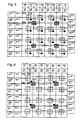
- Figures 5 and 6 show overviews of the described signals and states for the 2 ⁇ 2 and 4x4 (not claimed) binning modes, respectively.
- a sensor area of 8 ⁇ 8 pixels 1.11, 1.12, ..., 1.21, 1.22,... is shown; of course, the entire sensor might have a larger area and a larger number of pixels.
- Squares filled with dots represent pixels connected together in the 2 ⁇ 2 binning mode, hatched squares represent pixels connected together in the 4 ⁇ 4 binning mode (not claimed).
- the black dots indicate the pixels which are read (not claimed) out in the respective sensing nodes 7'.
- bin 4 ⁇ 4 0
- the line for 8 ⁇ 8 binning (not claimed) is fixed to ground on hardware base for reasons of simplicity, i.e., the binning is restricted to the 2x2 and 4x4 (not claimed) binning modes.
- This measure guarantees a similar neighborhood for all pixels (not claimed) 1.11, 1.12, ..., 1.21, 1.22, ... It also yields the advantage of smaller spacing between the photodiodes 2 if they are separated by depleted transistor channels.
- the method according to the invention is applied to groups of 2 ⁇ 2 pixels in a sensor having a 2 2n configuration, n being an integer.
Landscapes
- Engineering & Computer Science (AREA)
- Multimedia (AREA)
- Signal Processing (AREA)
- Transforming Light Signals Into Electric Signals (AREA)
- Solid State Image Pick-Up Elements (AREA)
Description
- The invention relates to a method for detecting light using an optoelectronic sensor.
- To date, two principles for solid-state image sensors prevail: charge-coupled-device (CCD) sensors and active-pixel sensors (APS). CCD sensors need a special manufacturing technology and have a relatively high power consumption. On the other hand, with CCD image sensors it is possible to increase the light sensitivity by concentrating in one single pixel the electric charge generated in several pixels. By doing this, the spatial resolution is reduced, but also the readout time and the power consumption are reduced. Thus CCDs can exploit the photocharge detection sensitivity of one pixel and the photocharge collection capability of many adjacent pixels. This operation mode called "charge binning" is described, e.g., in P. Seitz et al., "Smart optical and image sensors fabricated with industrial CMOS/CCD semiconductor processes", SPIE Vol. 1900, pp. 21-30, 2-3 February 1993. However, the readout time, or the power consumption (for a constant frame frequency), cannot be reduced by the same factor as the spatial resolution, because for a readout it is necessary to drive the whole sensor.
- APS sensors have the advantage of being realizable with standard complementary metal oxide semiconductor (CMOS) processes and of showing a relatively low power consumption. In an APS sensor, in each pixel the charge or current generated by the photodetector is actively converted into a voltage or current signal. Each pixel can be addressed and read out individually. It is possible with APS sensors to increase the readout velocity and/or the power consumption by reducing the spatial resolution. To date, it was however not possible to increase the light sensitivity of a pixel by interconnecting several pixels of an APS sensor. Of course it is possible to connect CMOS pixels with suitably placed MOS-FET switches to form one big "super-pixel". Although the effective photocharge collection area is enlarged in this way, the CMOS pixels find themselves all connected in parallel, enlarging the total capacitance of the "super-pixel". No mechanism has been known to force the distributed photocharge from the "super-pixel" into one CMOS pixel for sensitive charge detection in this pixel.
-
- It is therefore the aim of the invention to provide further aim of the invention to provide a method for detecting light with diode-based photodetectors which makes photocharge binning possible. These problems are solved by the the method as defined in the independent claim.
- The inventive method uses:
- a suitable topology of, preferably, CMOS pixels (with photodiode, reset gate and charge detector circuit) which are interconnected with MOS-FET switches controlled from the outside;
- special charge detection circuits which have an additional MOS-FET ("skimmer") at their inputs, offering a floating source and floating drain; and
- an operation mode in which the MOS-FET switches can be controlled to interconnect the pixels, and the skimming MOS-FET's gate is set to a DC potential which lies below the charge detection circuit's reset voltage.
- The optoelectronic sensor used in the method according to the invention comprises four pixels, each pixel comprising a photo-diode for generating an electric photocharge as a function of incident electromagnetic radiation, and means for electrically connecting said pixels, said connecting means comprising means for switching the connection on or off. Said pixels are designed in such a way that if they are connected the photocharges generated in said connected pixels are combined in one of said connected pixels, whereby the spatial resolution of the sensor is reduced.
- The method according to the invention for detecting electromagnetic radiation using the optoelectronic sensor according to the invention comprises the steps of generating an electric photocharge as a function of incoming electromagnetic radiation, and electrically connecting four pixels. The photocharges generated in said connected pixels are combined in one of said connected pixels, whereby the spatial resolution of the sensor is reduced.
- In this document, the term "light" is used for any kind of electromagnetic radiation, such as visible light, infrared (IR) or ultraviolet (UV) radiation.
- The invention makes it possible to vary the spatial resolution, the light sensitivity and/or the readout velocity by purely electronic means. The sensor can be manufactured in any CMOS technology without adding modified or additional steps. Its total readout time and/or its power consumption can be reduced by reducing the spatial resolution. In the sensor, groups of pixels are preferably isolated from each other by a depleted transistor channel which may also be switched into a conductive state, thus increasing the light sensitivity of a "super-pixel" composed of several pixels. Thus in the image sensor the light sensitivity or the spatial resolution can be varied purely electronically.
- Reducing the spatial resolution by connecting pixels according to the invention has the advantage of an increased light sensitivity, and, moreover, of being offset free because the signal of each pixel is read out via the same sensing node. This does not hold if the reduction of the resolution is only carried out by averaging after reading out.
- The power consumption of the sensor is reduced at a constant frame frequency if the spatial resolution is reduced, because only those pixels have to be supplied with voltage which effectively have to be read out.
- The invention also encompasses applying the claimed method to an architecture of control lines for controlling connecting switches between pixels in a two-dimensional sensor. With this architecture, square fields with 22n (= 4, 16, 64, ...) pixels, where n = 1, 2, 3, ... is an integer, can be formed by control lines oriented in one single direction.
- In the following, the invention and, for comparison, the state of the art are described in greater detail with reference to the accompanying drawings, wherein show:
- Fig. 1
- a basic circuit diagram of an APS sensor according to the state of the art;
- Fig. 2
- a basic circuit diagram of a sensor used in the method according to the invention;
- Fig. 3
- a more detailed basic circuit diagram of the sensor of
Fig. 2 ; - Fig. 4
- a schematic of an analogue gate pixel;
- Fig. 5
- the state of signals for skimming binning and reset for a sensor with 2×2 binning;
- Fig. 6
- the state of signals for skimming binning and reset for a sensor with 4x4 binning;
- Fig. 7
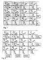
- an interleaved arrangement of a circuit for connecting pixels in a sensor ; and
- Fig. 8
- a circuit of connecting switches with horizontally and vertically separated addressing in a sensor.
-
Figure 1 shows a basic circuit diagram of an APS sensor according to the state of the art. Each pixel 101.11, 101.12, 101.21, 101.22, ... can be addressed and read out individually. In each pixel 101.11, 101.12, 101.21, 101.22, ... the charge or current generated by aphotodetector 102 is actively converted into a voltage or current signal by an output amplifier oroutput buffer 104, e.g., by a field effect transistor (FET) as a source follower. Thephotodetector 102 can be reset by aswitch 105. VDD designates a supply voltage, VSS a ground voltage, Vres a reset voltage and RS a reset signal. -
Figures 2 and3 show a sensor that can be used in the method of the invention. A plurality of pixels 1.11, 1.12, 1.21, 1.22 is assembled in order to form an image or array sensor. The pixels 1.11, 1.12, 1.21, 1.22 are addressed and read out individually. In the example ofFigs. 2 and3 , four pixels 1.11, 1.12, 1.21, 1.22 are connected to form a square field or "super-pixel". In each pixel 1.11, 1.12, 1.21, 1.22 incident light is converted by a photodiode into a photocurrent. A field effect transistor (FET) 3 with a constant gate voltage connects thephotodetector 2 with asensing node 7; for reasons explained below, thisFET 3 will be called the "skimming FET". An input of an output amplifier oroutput buffer 4, viz. the gate of a FET called the "amplifier FET" or "source follower FET", is connected to thesensing node 7. Thesensing node 7 can be set to the reset voltage Vres by aswitch 5, viz. a further FET called the "reset FET". By connections which can be switched on or off byfurther switches 6, also realized as FETs called the "binning FETs", output ports or "summing nodes" 8 of several pixels 1.11, 1.12, 1.21, 1.22 can be connected. - The photocurrent flows from the
photodetector 2 via theskimming FET 3 to thesensing node 7 and is integrated on the capacity of thesensing node 7. For this purpose, the parasitic depletion-layer capacitances of theFETs 3 connected to thesensing nodes 7 are preferably used. Thesource follower FET 4 is arranged according to the state of the art in such a way that the signal of thesensing node 7 can be further processed. After having been read out, a pixel 1.11, 1.12, 1.21, 1.22 is reset by thereset FET 5 to the reset voltage Vres. - Generally, the voltage signal generated at a
sensing node 7 is inversely proportional to the capacitance of thisnode 7. If thesensing node 7 is connected directly to thephotodiode 2 as inFig. 1 , the voltage at thenode 7 is given by
where I photo is the photocurrent generated in thephotodiode 2, T int the integration time, C sensnode the parasitic capacitance of thesensing node 7 and C diode the parasitic capacitance of thephotodiode 2. Since the parasitic capacitance C diode of thephotodiode 2 is directly proportional to the light-sensitive area of thephotodiode 2, it cannot be reduced arbitrarily. Due to this fact, the light sensitivity is limited. - By using a FET, i.e., the
skimming FET 3, as a connection between thephotodiode 2 and thesensing node 7, the parasitic capacitance of thephotodiode 2 is separated from thesensing node 7. In order to increase the light sensitivity, the gate voltage of the skimmingFET 3 is chosen in such a way that the voltage at the output of thephotodiode 2 remains constant at all times and upon a reset only the capacitance of thesensing node 7 is depleted. Thus the voltage at thesensing node 7 is given by
- A further increase of the light sensitivity is achieved according to the invention by reducing the spatial resolution and guiding the photocurrent from
several photodiodes 2, i.e., from several pixels 1.11, 1.12, 1.21, 1.22, to one single sensing node 7' viz. of the pixel 1.22. For this purpose the output ports of the pixels 1.11, 1.12, 1.21, 1.22 are connected to each other by switches, viz. the binningFETs 6, thus forming a group, field or "super-pixel" of, e.g., 2×2 pixels 1.11, 1.12, 1.21, 1.22. Thus the number of pixels is reduced and their effective, light-sensitive area is increased; however, the parasitic capacity of thesensing nodes 7 remains constant. In order to transfer the photogenerated charges of the connected photodiodes to one sensing node 7', in each "super-pixel" only the sensing node 7' which is read out is reset to the reset voltage Vres. This is accomplished by addressingreset switches 5 andskimming switches 3 in a bi-directional way, e.g., resetswitches 5 in row direction and skimmingswitches 3 in column direction. In this case the voltage signal at the sensing node 7' is given by
- The signal deviation increases, in a not-claimed example, when the number of connected pixels 1.11, 1.12, 1.21, 1.22 increases, i.e., when the spatial resolution of the image or array sensor decreases. Thus in the image sensor the light sensitivity or the spatial resolution can be varied purely electronically.
- In CMOS technologies, zones of various types of semiconductor material (p-type and n-type Silicon) can be produced. Today these zones are typically, however not exclusively, produced by implantation of appropriate doping atoms into the Silicon substrate. By using such doping (source/drain implant) in combination with a thin conductor (poly Silicon) which is separated by a thin isolator (gate oxide), FETs are produced in CMOS technologies. The source and drain regions of such FETs are also charge-accumulating regions and can be used as photodiodes.
- In the sensor, such FETs are used for separating the optically active areas of the detector elements from each other at a minimum distance. The detector elements are formed and/or contacted by source- and drain-implanted regions of the FETs. The channel zones of these FETs are depleted by applying an appropriate potential at the FET gate and separate the individual detector elements electrically from each other.
-
Figure 4 shows a more detailed circuit which can be used in apixel 1 of the sensor In order to reduce the capacitance of thesensing node 7, thephotodiode 2 is separated from thesensing node 7 by a simple MOS transistor, e.g., theskimming FET 3, with a suitable analogue gate voltage. Therefore, apixel 1 containing this circuit may be called an "analogue gate pixel" (AGP). There may be a further transistor between the skimmingFET 3 and thesensing node 7 for performing an electronic shutter function. A still further switch or transistor 10 at the output of thesource follower FET 4 can be used as a row selector. The supply voltage VDD and the reset voltage Vres can be identical, i.e., short-circuited together. - In order to dispense with additional signal lines for connecting individual pixels 1.11, 1.12, 1.21, 1.22,..., the 2 are designed as source- and drain-implanted regions of the connecting switches 6 (binning FETs), or are designed so as to overlap with these regions. For variably reducing the spatial resolution of the sensor, it is merely necessary to additionally introduce control lines (gate terminals of the binning FETs 6) for the connecting switches 6.
- Turning again to
Figure 3 , the readout addressing of the sensor is explained. Generally in an APS sensor, there is a signal bus in column direction. The outputs of each pixel in the corresponding column are connected to this bus via a row select transistor (seeFig. 4 , FET 10). The row select transistors of a row are controlled by a signal line in the row direction. With this arrangement, it is possible to address each individual pixel in the sensor by choosing a certain column and a certain row. After reading out a row of pixels, the voltage in the sensing nodes of these pixels is reset to a reset voltage Vres by putting thereset transistors 5 into a conductive state. Theseswitches 5 are preferably also connected in the row direction. In the sensor shown inFig. 3 , the signals for thereset FETs 5 are connected in rows, whereas the signals for the skimmingFETs 3 are connected in columns and can be switched on, off or to an analogue voltage. The skimmingFETs 3 are used for the charge skimming and/or as shutter transistors to prevent a reset of thephotodiodes 2. - In order to perform charge binning, the sensor is switched from the regular mode to the binning mode for at least one frame or picture. The signals described hereafter are then once set to certain values and do not change any more until the binning mode is switched off. The following description of the binning mode refers to n-MOS transistors, which means that the switches 3-6, 9-10 conduct if the signals applied to their gates are high (VDD). The functionality for p-MOS transistors (not claimed) would be the same, but all signals would be inverted.
- First the 2x2 binning mode is described. In order to perform binning from four pixels 1.11, 1.12, 1.21, 1.22 to one "super-pixel" (2x2), the gate voltage of the 2x2 switches 6 is set to VDD and thus the 4 pixels 1.11, 1.12, 1.21, 1.22 are connected together. Now the pixel 7' from which the output signal is to be read out has to be chosen; this might be, e.g., the pixel 1.22 in
row 2, column B. A reset of thediodes 2 in any other pixel 1.11, 1.12, 1.21 must be avoided. Since thereset FETs 5 are connected in the row direction, such an unwanted reset in row 1 (pixels 1.11, 1.12) is avoided by fixing the gates of thereset FETs 5 in thisrow 1 to ground (VSS). In order to avoid the reset of thediode 2 in the pixel 1.21 inrow 2, column A, theskimming FET 3 in this pixel 1.21 must be blocked. This is done by setting the gate voltages of the skimmingFETs 3 of column A (pixels 1.11, 1.21) to ground (VSS). With these measures, the entire charge generated in the four photodiodes 1.11, 1.12, 1.21, 1.22 must go through the read-out pixel 1.22 inrow 2, column B. In order to take advantage of the charge skimming principle, and thus to increase the signal on the sensing node 7' of this read-out pixell.22, the potential of the skimmingFETs 3 in column B (pixels 1.12, 1.22) is set to an analogue voltage between VDD and VSS. It is evident that only reading out the output of the pixel 1.22 inrow 2, column B yields useful data. -
Figures 5 and 6 show overviews of the described signals and states for the 2×2 and 4x4 (not claimed) binning modes, respectively. In both figures, a sensor area of 8×8 pixels 1.11, 1.12, ..., 1.21, 1.22,... is shown; of course, the entire sensor might have a larger area and a larger number of pixels. Squares filled with dots represent pixels connected together in the 2×2 binning mode, hatched squares represent pixels connected together in the 4×4 binning mode (not claimed). The black dots indicate the pixels which are read (not claimed) out in the respective sensing nodes 7'. - The Skim signal is the signal used for the charge skimming FETs; "Skim = 0" means that the skimming
FETs 3 in this column are blocked (gates connected to VSS), whereas "Skim = an" means that in this column the gates of the skimmingFETs 3 are set to an analogue fixed voltage between VDD and VSS. "Reset = 0" means that in this row no reset is performed, i.e., the gates of thereset FETs 5 are set to VSS; "normal reset" means that in this row the reset is performed after the pixels in the row have been read out. "bin 2×2 = 1" means that the 2×2 binning mode is on, and that the gates of the binningFETs 6 used for this mode are connected to VDD or to an analogue voltage which lies between VDD and VSS but is higher than the analogue voltage of the skimmingFETs 3. "bin 4×4 = 0" and "bin 8×8 = 0" means that the corresponding lines are set to VSS or to ground, i.e., thecorresponding binning FETs 6 are blocked and do not allow photocharge binning. - In
Figs. 5 and 6 , the line for 8×8 binning (not claimed) is fixed to ground on hardware base for reasons of simplicity, i.e., the binning is restricted to the 2x2 and 4x4 (not claimed) binning modes. This measure guarantees a similar neighborhood for all pixels (not claimed) 1.11, 1.12, ..., 1.21, 1.22, ... It also yields the advantage of smaller spacing between thephotodiodes 2 if they are separated by depleted transistor channels. Of course, it is possible to provide lines and switches for 8×8, 16×16, ..., 2n×2i binning modes (not claimed). By an interleaved arrangement and control of the connecting switches 6 (binning FETs 6), "super-pixels" consisting of 22n (= 4, 16, 64, ...) connected pixels, where n = 1, 2, 3, ... is an integer, can simply be formed, as shown inFigure 7 (only the case n = 1 is used in the method according to the invention). - By separately controlling the horizontal and vertical connecting switches 6 (binning FETs 6), rectangular fields or "super-pixels" with pxq connected pixels, where p = 1, 2, 3... and q = 2, 3,...; or p=2,3,... and q = 1, 2, 3,... are integers, can be formed using well-known electronic components and techniques, as shown in
Figure 8 (only the case n = 1 is used in the method according to the invention). - In one embodiment, the method according to the invention is applied to groups of 2×2 pixels in a sensor having a 22n configuration, n being an integer.
Claims (2)
- A method for detecting electromagnetic radiation using an optoelectronic sensor comprising:a group of pixels that comprises four pixels (1.11, 1.12, 1.21, 1.22) which are arranged in a 2x2 row-and-column matrix configuration comprising a Row 1, a Row 2, a Column 1, and a Column 2;wherein each pixel (1.11, 1.12, 1.21, 1.22) comprises:a photodiode (2);an output n-MOS field effect transistor (FET) amplifier (4);a reset n-MOS FET switch (5);a skimming n-MOS FET (3);connecting means comprising a first binning n-MOS FET (6) and a second binning n-MOS FET (6);a sensing node (7) having parasitic capacitance;wherein the drain of said skimming FET (3) and the drain of said reset switch (5) are connected in parallel via said sensing node (7) to the gate of said output amplifier (4); andwherein the drain of the first binning FET (6) is connected to the source of said skimming FET (3);wherein the drains of the first and the second binning FETs are connected in parallel to the output of said photodiode (2) via a summing node (8); andwherein the drains of the second binning FETs comprised in the pixels of Column 1 at positions 1.11 and 1.21 are connected to the sources of the second binning FETs comprised in the pixels of Column 2 at positions 1.12 and 1.22, respectively,said method comprising a step of generating an electric photocharge as a function of incoming electromagnetic radiation, andsaid method being characterized by comprising the following steps, while maintaining the DC potentials of the gates of said skimming FETs (3) below the reset voltage of the output amplifier (4) of the respective pixel:a) setting the gate voltages of said binning FETs (6) to a supply voltage (VDD), resulting in that said pixels (1.11, 1.12, 1.21, 1.22) are connected together;b) setting the gate voltage of said reset switches (5) of the pixels (1.11, 1.12) in Row 1 to ground (VSS) to prevent reset of said pixels (1.11, 1.12) of Row 1; andc) blocking the skimming FET (3) of the pixel in Row 2 and column 1 (1.21) by setting the gate voltages of the skimming FETs (3) of Column 1 to ground (VSS) to prevent reset of the corresponding pixel (1.21), thereby causing photoelectric charges generated in the photodiodes (2) of said four pixels (1.11, 1.12, 1.21, 1.22) to be transferred to the output amplifier (4) of the pixel (7', 1.22) of Row 2 and Column 2;d) setting the potential of the gate voltage of the skimming FETs (3) respective of the pixels of Column 2 (1.21, 1.22) to an analogue voltage between the supply voltage (VDD) and the ground voltage (VSS); ande) reading out the output of the pixel 1.22 in Row 2, Column 2.
- The method for detecting electromagnetic radiation according to claim 1, comprising:f) performing, in a 22n pixel configuration, where n is an integer, for each separate group of 2x2 pixels, steps b) to e).
Priority Applications (2)
| Application Number | Priority Date | Filing Date | Title |
|---|---|---|---|
| EP99811074A EP1102323B1 (en) | 1999-11-19 | 1999-11-19 | Method for detecting electromagnetic radiation using an optoelectronic sensor |
| US09/716,168 US6452153B1 (en) | 1999-11-19 | 2000-11-17 | Optoelectronic sensor |
Applications Claiming Priority (1)
| Application Number | Priority Date | Filing Date | Title |
|---|---|---|---|
| EP99811074A EP1102323B1 (en) | 1999-11-19 | 1999-11-19 | Method for detecting electromagnetic radiation using an optoelectronic sensor |
Publications (2)
| Publication Number | Publication Date |
|---|---|
| EP1102323A1 EP1102323A1 (en) | 2001-05-23 |
| EP1102323B1 true EP1102323B1 (en) | 2012-08-15 |
Family
ID=8243155
Family Applications (1)
| Application Number | Title | Priority Date | Filing Date |
|---|---|---|---|
| EP99811074A Expired - Lifetime EP1102323B1 (en) | 1999-11-19 | 1999-11-19 | Method for detecting electromagnetic radiation using an optoelectronic sensor |
Country Status (2)
| Country | Link |
|---|---|
| US (1) | US6452153B1 (en) |
| EP (1) | EP1102323B1 (en) |
Cited By (1)
| Publication number | Priority date | Publication date | Assignee | Title |
|---|---|---|---|---|
| US11463644B2 (en) | 2018-08-31 | 2022-10-04 | Canon Kabushiki Kaisha | Imaging device, imaging system, and drive method of imaging device |
Families Citing this family (56)
| Publication number | Priority date | Publication date | Assignee | Title |
|---|---|---|---|---|
| US6956605B1 (en) * | 1998-08-05 | 2005-10-18 | Canon Kabushiki Kaisha | Image pickup apparatus |
| DE19947536A1 (en) * | 1999-10-02 | 2001-04-05 | Philips Corp Intellectual Pty | Sensor array read-out method e.g. for diagnostic X-ray imaging, has controlled switches between adjacent addressing lines and adjacent read-out lines |
| GB9930257D0 (en) * | 1999-12-22 | 2000-02-09 | Suisse Electronique Microtech | Optoelectronic sensor |
| EP1143706A3 (en) * | 2000-03-28 | 2007-08-01 | Fujitsu Limited | Image sensor with black level control and low power consumption |
| AU2002213702A1 (en) * | 2000-10-30 | 2002-05-15 | Simon Fraser University | Active pixel sensor with built in self-repair and redundancy |
| JP2002320235A (en) * | 2001-04-19 | 2002-10-31 | Fujitsu Ltd | A CMOS image sensor that generates a reduced image signal while suppressing a decrease in spatial resolution |
| US6914227B2 (en) * | 2001-06-25 | 2005-07-05 | Canon Kabushiki Kaisha | Image sensing apparatus capable of outputting image by converting resolution by adding and reading out a plurality of pixels, its control method, and image sensing system |
| JP3965049B2 (en) * | 2001-12-21 | 2007-08-22 | 浜松ホトニクス株式会社 | Imaging device |
| US7361881B2 (en) * | 2002-03-13 | 2008-04-22 | Oy Ajat Ltd | Ganged detector pixel, photon/pulse counting radiation imaging device |
| JP4246964B2 (en) | 2002-05-27 | 2009-04-02 | 浜松ホトニクス株式会社 | Solid-state imaging device and solid-state imaging device array |
| JP4302362B2 (en) * | 2002-06-21 | 2009-07-22 | 富士フイルム株式会社 | Solid-state imaging device |
| US7304674B2 (en) * | 2002-11-15 | 2007-12-04 | Avago Technologies General Ip Pte Ltd | Sampling image signals generated by pixel circuits of an active pixel sensor (APS) image sensor in a sub-sampling mode |
| FR2847677B1 (en) | 2002-11-26 | 2005-01-07 | Commissariat Energie Atomique | PARTICLE DETECTOR AND COUNTER DEVICE COMPRISING A PLURALITY OF PARTICLE DETECTORS |
| US6878918B2 (en) * | 2003-01-09 | 2005-04-12 | Dialdg Semiconductor Gmbh | APS pixel with reset noise suppression and programmable binning capability |
| JP4562997B2 (en) * | 2003-03-26 | 2010-10-13 | 株式会社半導体エネルギー研究所 | Element substrate and light emitting device |
| WO2004086343A1 (en) | 2003-03-26 | 2004-10-07 | Semiconductor Energy Laboratory Co., Ltd. | Device substrate and light-emitting device |
| US7859581B2 (en) * | 2003-07-15 | 2010-12-28 | Eastman Kodak Company | Image sensor with charge binning and dual channel readout |
| US7408195B2 (en) * | 2003-09-04 | 2008-08-05 | Cypress Semiconductor Corporation (Belgium) Bvba | Semiconductor pixel arrays with reduced sensitivity to defects |
| US7091466B2 (en) * | 2003-12-19 | 2006-08-15 | Micron Technology, Inc. | Apparatus and method for pixel binning in an image sensor |
| US7471327B2 (en) | 2004-01-21 | 2008-12-30 | Xerox Corporation | Image sensor array with variable resolution and high-speed output |
| WO2005107235A1 (en) * | 2004-05-05 | 2005-11-10 | Koninklijke Philips Electronics N.V. | Electronic device with an array of processing units |
| KR100680469B1 (en) | 2005-01-31 | 2007-02-08 | 매그나칩 반도체 유한회사 | CMOS image sensor with sensing nodes shared between adjacent pixels |
| US7611060B2 (en) | 2005-03-11 | 2009-11-03 | Hand Held Products, Inc. | System and method to automatically focus an image reader |
| US7780089B2 (en) | 2005-06-03 | 2010-08-24 | Hand Held Products, Inc. | Digital picture taking optical reader having hybrid monochrome and color image sensor array |
| US7568628B2 (en) | 2005-03-11 | 2009-08-04 | Hand Held Products, Inc. | Bar code reading device with global electronic shutter control |
| US7705900B2 (en) | 2005-06-01 | 2010-04-27 | Eastman Kodak Company | CMOS image sensor pixel with selectable binning and conversion gain |
| US7770799B2 (en) | 2005-06-03 | 2010-08-10 | Hand Held Products, Inc. | Optical reader having reduced specular reflection read failures |
| DE102005049228B4 (en) * | 2005-10-14 | 2014-03-27 | Siemens Aktiengesellschaft | Detector with an array of photodiodes |
| US20070285547A1 (en) * | 2006-05-30 | 2007-12-13 | Milligan Edward S | CMOS image sensor array optimization for both bright and low light conditions |
| US7764315B2 (en) * | 2006-08-24 | 2010-07-27 | Dalsa Corporation | CMOS imaging facility and a modular array for use in such a facility |
| US8031249B2 (en) | 2007-01-11 | 2011-10-04 | Micron Technology, Inc. | Missing pixel architecture |
| JP5187550B2 (en) * | 2007-08-21 | 2013-04-24 | ソニー株式会社 | Imaging device |
| EP2154879A1 (en) * | 2008-08-13 | 2010-02-17 | Thomson Licensing | CMOS image sensor with selectable hard-wired binning |
| US7777171B2 (en) * | 2008-08-26 | 2010-08-17 | Eastman Kodak Company | In-pixel summing of charge generated by two or more pixels having two reset transistors connected in series |
| US8913166B2 (en) | 2009-01-21 | 2014-12-16 | Canon Kabushiki Kaisha | Solid-state imaging apparatus |
| TWI423673B (en) * | 2011-03-17 | 2014-01-11 | Innolux Corp | Image sensing pixel and driving method thereof |
| FR2977371B1 (en) * | 2011-06-30 | 2013-08-02 | Trixell | PIXEL MATRIX WITH PROGRAMMABLE GROUPS |
| DE102011107844A1 (en) * | 2011-07-01 | 2013-01-03 | Heinrich Schemmann | CMOS image sensor with fixed pixel binning through various interconnections |
| JP6039165B2 (en) * | 2011-08-11 | 2016-12-07 | キヤノン株式会社 | Imaging device and imaging apparatus |
| FR2979485B1 (en) | 2011-08-26 | 2016-09-09 | E2V Semiconductors | PIXEL REGROUPING IMAGE SENSOR |
| JP6080411B2 (en) * | 2012-07-13 | 2017-02-15 | キヤノン株式会社 | Imaging device, driving method of imaging device, and driving method of imaging system |
| JP2014209696A (en) | 2012-07-23 | 2014-11-06 | ソニー株式会社 | Solid-state imaging device, signal reading method, and electronic apparatus |
| KR102087225B1 (en) * | 2013-05-30 | 2020-03-11 | 에스케이하이닉스 주식회사 | Image sensing device |
| US9729809B2 (en) * | 2014-07-11 | 2017-08-08 | Semiconductor Energy Laboratory Co., Ltd. | Semiconductor device and driving method of semiconductor device or electronic device |
| KR20170056909A (en) | 2015-11-16 | 2017-05-24 | 삼성전자주식회사 | Image sensor and electronic device having the same |
| JP7299702B2 (en) * | 2016-09-29 | 2023-06-28 | 株式会社ニコン | Image sensor and electronic camera |
| US11006056B2 (en) * | 2017-01-31 | 2021-05-11 | Nikon Corporation | Image sensor and image-capturing device with pixels having amplifiers |
| US11509841B2 (en) | 2017-01-31 | 2022-11-22 | Nikon Corporation | Image sensor and image-capturing device with first and second amplifiers connectable to each other's current sources |
| CN110393007B (en) * | 2017-01-31 | 2021-11-26 | 株式会社尼康 | Image pickup element and image pickup apparatus |
| JP6809543B2 (en) * | 2017-01-31 | 2021-01-06 | 株式会社ニコン | Image sensor and electronic camera |
| JP6910009B2 (en) * | 2017-02-03 | 2021-07-28 | パナソニックIpマネジメント株式会社 | Imaging equipment and camera system |
| US10175087B2 (en) * | 2017-02-09 | 2019-01-08 | The Boeing Company | Fuel level sensor having dual fluorescent plastic optical fibers |
| US10192911B2 (en) * | 2017-05-09 | 2019-01-29 | Apple Inc. | Hybrid image sensors with improved charge injection efficiency |
| JP2019092022A (en) * | 2017-11-14 | 2019-06-13 | ソニーセミコンダクタソリューションズ株式会社 | Imaging apparatus, imaging method, and imaging system |
| JP7356266B2 (en) * | 2018-08-31 | 2023-10-04 | キヤノン株式会社 | Imaging device, imaging system, and method for driving the imaging device |
| WO2025235163A1 (en) * | 2024-05-08 | 2025-11-13 | Apple Inc. | Foveated sensor readout |
Family Cites Families (6)
| Publication number | Priority date | Publication date | Assignee | Title |
|---|---|---|---|---|
| US5909026A (en) * | 1996-11-12 | 1999-06-01 | California Institute Of Technology | Integrated sensor with frame memory and programmable resolution for light adaptive imaging |
| DE19715214C1 (en) * | 1997-04-11 | 1998-07-02 | Siemens Ag | Image sensor with several image point sensor regions |
| US6107655A (en) * | 1997-08-15 | 2000-08-22 | Eastman Kodak Company | Active pixel image sensor with shared amplifier read-out |
| US6714239B2 (en) * | 1997-10-29 | 2004-03-30 | Eastman Kodak Company | Active pixel sensor with programmable color balance |
| US6977684B1 (en) * | 1998-04-30 | 2005-12-20 | Canon Kabushiki Kaisha | Arrangement of circuits in pixels, each circuit shared by a plurality of pixels, in image sensing apparatus |
| US6665012B1 (en) * | 1998-09-22 | 2003-12-16 | Pixim, Inc. | Process-scalable high spatial resolution and low bit resolution CMOS area image sensor |
-
1999
- 1999-11-19 EP EP99811074A patent/EP1102323B1/en not_active Expired - Lifetime
-
2000
- 2000-11-17 US US09/716,168 patent/US6452153B1/en not_active Expired - Fee Related
Cited By (1)
| Publication number | Priority date | Publication date | Assignee | Title |
|---|---|---|---|---|
| US11463644B2 (en) | 2018-08-31 | 2022-10-04 | Canon Kabushiki Kaisha | Imaging device, imaging system, and drive method of imaging device |
Also Published As
| Publication number | Publication date |
|---|---|
| EP1102323A1 (en) | 2001-05-23 |
| US6452153B1 (en) | 2002-09-17 |
Similar Documents
| Publication | Publication Date | Title |
|---|---|---|
| US6452153B1 (en) | Optoelectronic sensor | |
| US6603513B1 (en) | Using a single control line to provide select and reset signals to image sensors in two rows of a digital imaging device | |
| EP1900191B1 (en) | Cmos image sensor pixel with selectable binning | |
| US5182623A (en) | Charge coupled device/charge super sweep image system and method for making | |
| CN1200555C (en) | Active linear sensor | |
| US5471515A (en) | Active pixel sensor with intra-pixel charge transfer | |
| EP0862219B1 (en) | Active pixel sensor in which adjacent pixels share an integrated electrical element | |
| EP0964570B1 (en) | Solid-state imaging element | |
| US8174601B2 (en) | Image sensor with controllable transfer gate off state voltage levels | |
| US8436288B2 (en) | Image sensors with photo-current mode and solar cell operation | |
| US5430481A (en) | Multimode frame transfer image sensor | |
| US7807955B2 (en) | Image sensor having reduced well bounce | |
| EP1583150A1 (en) | Image sensor with large-area, high-sensitivity and high-speed pixels | |
| Hynecek | A new device architecture suitable for high-resolution and high-performance image sensors | |
| EP2041958B1 (en) | Ccd with improved substrate voltage setting circuit | |
| US7408195B2 (en) | Semiconductor pixel arrays with reduced sensitivity to defects | |
| US5748232A (en) | Image sensor and driving method for the same | |
| JP3675984B2 (en) | Light receiving element circuit and light receiving element circuit array | |
| EP0565775B1 (en) | Solid-state imaging device | |
| EP0216426B1 (en) | Imaging devices comprising photovoltaic detector elements | |
| EP0215531B1 (en) | Imaging devices comprising photodetector elements | |
| JP3447326B2 (en) | Solid-state imaging device | |
| WO2002063691A2 (en) | Active pixel cell with charge storage | |
| US20070063232A1 (en) | Solid-state imaging device | |
| KR100683396B1 (en) | Pixel array scanning method of image sensor |
Legal Events
| Date | Code | Title | Description |
|---|---|---|---|
| PUAI | Public reference made under article 153(3) epc to a published international application that has entered the european phase |
Free format text: ORIGINAL CODE: 0009012 |
|
| AK | Designated contracting states |
Kind code of ref document: A1 Designated state(s): AT BE CH CY DE DK ES FI FR GB GR IE IT LI LU MC NL PT SE |
|
| AX | Request for extension of the european patent |
Free format text: AL;LT;LV;MK;RO;SI |
|
| 17P | Request for examination filed |
Effective date: 20011112 |
|
| AKX | Designation fees paid |
Free format text: AT BE CH CY DE DK ES FI FR GB GR IE IT LI LU MC NL PT SE |
|
| RAP1 | Party data changed (applicant data changed or rights of an application transferred) |
Owner name: CSEM CENTRE SUISSE D'ELECTRONIQUE ET DE MICROTECHN |
|
| RTI1 | Title (correction) |
Free format text: METHOD FOR DETECTING ELECTROMAGNETIC RADIATION USING AN OPTOELECTRONIC SENSOR |
|
| GRAP | Despatch of communication of intention to grant a patent |
Free format text: ORIGINAL CODE: EPIDOSNIGR1 |
|
| GRAS | Grant fee paid |
Free format text: ORIGINAL CODE: EPIDOSNIGR3 |
|
| GRAA | (expected) grant |
Free format text: ORIGINAL CODE: 0009210 |
|
| AK | Designated contracting states |
Kind code of ref document: B1 Designated state(s): AT BE CH CY DE DK ES FI FR GB GR IE IT LI LU MC NL PT SE |
|
| REG | Reference to a national code |
Ref country code: AT Ref legal event code: REF Ref document number: 571218 Country of ref document: AT Kind code of ref document: T Effective date: 20120815 Ref country code: GB Ref legal event code: FG4D Ref country code: CH Ref legal event code: EP |
|
| REG | Reference to a national code |
Ref country code: IE Ref legal event code: FG4D |
|
| REG | Reference to a national code |
Ref country code: DE Ref legal event code: R096 Ref document number: 69944353 Country of ref document: DE Effective date: 20121011 |
|
| REG | Reference to a national code |
Ref country code: CH Ref legal event code: NV Representative=s name: SCHNEIDER FELDMANN AG PATENT- UND MARKENANWAEL, CH |
|
| REG | Reference to a national code |
Ref country code: NL Ref legal event code: VDEP Effective date: 20120815 |
|
| REG | Reference to a national code |
Ref country code: AT Ref legal event code: MK05 Ref document number: 571218 Country of ref document: AT Kind code of ref document: T Effective date: 20120815 |
|
| PG25 | Lapsed in a contracting state [announced via postgrant information from national office to epo] |
Ref country code: FI Free format text: LAPSE BECAUSE OF FAILURE TO SUBMIT A TRANSLATION OF THE DESCRIPTION OR TO PAY THE FEE WITHIN THE PRESCRIBED TIME-LIMIT Effective date: 20120815 Ref country code: AT Free format text: LAPSE BECAUSE OF FAILURE TO SUBMIT A TRANSLATION OF THE DESCRIPTION OR TO PAY THE FEE WITHIN THE PRESCRIBED TIME-LIMIT Effective date: 20120815 Ref country code: CY Free format text: LAPSE BECAUSE OF FAILURE TO SUBMIT A TRANSLATION OF THE DESCRIPTION OR TO PAY THE FEE WITHIN THE PRESCRIBED TIME-LIMIT Effective date: 20120815 |
|
| PG25 | Lapsed in a contracting state [announced via postgrant information from national office to epo] |
Ref country code: GR Free format text: LAPSE BECAUSE OF FAILURE TO SUBMIT A TRANSLATION OF THE DESCRIPTION OR TO PAY THE FEE WITHIN THE PRESCRIBED TIME-LIMIT Effective date: 20121116 Ref country code: PT Free format text: LAPSE BECAUSE OF FAILURE TO SUBMIT A TRANSLATION OF THE DESCRIPTION OR TO PAY THE FEE WITHIN THE PRESCRIBED TIME-LIMIT Effective date: 20121217 Ref country code: BE Free format text: LAPSE BECAUSE OF FAILURE TO SUBMIT A TRANSLATION OF THE DESCRIPTION OR TO PAY THE FEE WITHIN THE PRESCRIBED TIME-LIMIT Effective date: 20120815 Ref country code: SE Free format text: LAPSE BECAUSE OF FAILURE TO SUBMIT A TRANSLATION OF THE DESCRIPTION OR TO PAY THE FEE WITHIN THE PRESCRIBED TIME-LIMIT Effective date: 20120815 |
|
| PG25 | Lapsed in a contracting state [announced via postgrant information from national office to epo] |
Ref country code: NL Free format text: LAPSE BECAUSE OF FAILURE TO SUBMIT A TRANSLATION OF THE DESCRIPTION OR TO PAY THE FEE WITHIN THE PRESCRIBED TIME-LIMIT Effective date: 20120815 |
|
| PG25 | Lapsed in a contracting state [announced via postgrant information from national office to epo] |
Ref country code: ES Free format text: LAPSE BECAUSE OF FAILURE TO SUBMIT A TRANSLATION OF THE DESCRIPTION OR TO PAY THE FEE WITHIN THE PRESCRIBED TIME-LIMIT Effective date: 20121126 Ref country code: DK Free format text: LAPSE BECAUSE OF FAILURE TO SUBMIT A TRANSLATION OF THE DESCRIPTION OR TO PAY THE FEE WITHIN THE PRESCRIBED TIME-LIMIT Effective date: 20120815 |
|
| PG25 | Lapsed in a contracting state [announced via postgrant information from national office to epo] |
Ref country code: IT Free format text: LAPSE BECAUSE OF FAILURE TO SUBMIT A TRANSLATION OF THE DESCRIPTION OR TO PAY THE FEE WITHIN THE PRESCRIBED TIME-LIMIT Effective date: 20120815 |
|
| PLBE | No opposition filed within time limit |
Free format text: ORIGINAL CODE: 0009261 |
|
| STAA | Information on the status of an ep patent application or granted ep patent |
Free format text: STATUS: NO OPPOSITION FILED WITHIN TIME LIMIT |
|
| 26N | No opposition filed |
Effective date: 20130516 |
|
| REG | Reference to a national code |
Ref country code: IE Ref legal event code: MM4A |
|
| REG | Reference to a national code |
Ref country code: DE Ref legal event code: R097 Ref document number: 69944353 Country of ref document: DE Effective date: 20130516 |
|
| PG25 | Lapsed in a contracting state [announced via postgrant information from national office to epo] |
Ref country code: IE Free format text: LAPSE BECAUSE OF NON-PAYMENT OF DUE FEES Effective date: 20121119 |
|
| PGFP | Annual fee paid to national office [announced via postgrant information from national office to epo] |
Ref country code: GB Payment date: 20131127 Year of fee payment: 15 Ref country code: DE Payment date: 20131127 Year of fee payment: 15 |
|
| PGFP | Annual fee paid to national office [announced via postgrant information from national office to epo] |
Ref country code: FR Payment date: 20131127 Year of fee payment: 15 |
|
| PG25 | Lapsed in a contracting state [announced via postgrant information from national office to epo] |
Ref country code: MC Free format text: LAPSE BECAUSE OF NON-PAYMENT OF DUE FEES Effective date: 20121130 |
|
| PG25 | Lapsed in a contracting state [announced via postgrant information from national office to epo] |
Ref country code: LU Free format text: LAPSE BECAUSE OF NON-PAYMENT OF DUE FEES Effective date: 20121119 |
|
| REG | Reference to a national code |
Ref country code: DE Ref legal event code: R082 Ref document number: 69944353 Country of ref document: DE Representative=s name: SCHAUMBURG UND PARTNER PATENTANWAELTE MBB, DE Ref country code: DE Ref legal event code: R082 Ref document number: 69944353 Country of ref document: DE Representative=s name: SCHAUMBURG & PARTNER PATENTANWAELTE GBR, DE |
|
| REG | Reference to a national code |
Ref country code: DE Ref legal event code: R119 Ref document number: 69944353 Country of ref document: DE |
|
| GBPC | Gb: european patent ceased through non-payment of renewal fee |
Effective date: 20141119 |
|
| REG | Reference to a national code |
Ref country code: FR Ref legal event code: ST Effective date: 20150731 |
|
| PG25 | Lapsed in a contracting state [announced via postgrant information from national office to epo] |
Ref country code: GB Free format text: LAPSE BECAUSE OF NON-PAYMENT OF DUE FEES Effective date: 20141119 Ref country code: DE Free format text: LAPSE BECAUSE OF NON-PAYMENT OF DUE FEES Effective date: 20150602 |
|
| PG25 | Lapsed in a contracting state [announced via postgrant information from national office to epo] |
Ref country code: FR Free format text: LAPSE BECAUSE OF NON-PAYMENT OF DUE FEES Effective date: 20141201 |
|
| PGFP | Annual fee paid to national office [announced via postgrant information from national office to epo] |
Ref country code: CH Payment date: 20151123 Year of fee payment: 17 |
|
| REG | Reference to a national code |
Ref country code: CH Ref legal event code: PL |
|
| PG25 | Lapsed in a contracting state [announced via postgrant information from national office to epo] |
Ref country code: CH Free format text: LAPSE BECAUSE OF NON-PAYMENT OF DUE FEES Effective date: 20161130 Ref country code: LI Free format text: LAPSE BECAUSE OF NON-PAYMENT OF DUE FEES Effective date: 20161130 |