EP1102096A2 - Optical crossconnect using tilting mirror MEMS array - Google Patents
Optical crossconnect using tilting mirror MEMS array Download PDFInfo
- Publication number
- EP1102096A2 EP1102096A2 EP00309821A EP00309821A EP1102096A2 EP 1102096 A2 EP1102096 A2 EP 1102096A2 EP 00309821 A EP00309821 A EP 00309821A EP 00309821 A EP00309821 A EP 00309821A EP 1102096 A2 EP1102096 A2 EP 1102096A2
- Authority
- EP
- European Patent Office
- Prior art keywords
- array
- optical signals
- output
- input
- mirror
- Prior art date
- Legal status (The legal status is an assumption and is not a legal conclusion. Google has not performed a legal analysis and makes no representation as to the accuracy of the status listed.)
- Granted
Links
- 230000003287 optical effect Effects 0.000 title claims abstract description 77
- 239000000835 fiber Substances 0.000 claims abstract description 62
- 238000003491 array Methods 0.000 claims abstract description 30
- 239000000758 substrate Substances 0.000 claims description 9
- 238000004891 communication Methods 0.000 claims description 8
- 238000010276 construction Methods 0.000 description 2
- 230000008878 coupling Effects 0.000 description 2
- 238000010168 coupling process Methods 0.000 description 2
- 238000005859 coupling reaction Methods 0.000 description 2
- 238000000034 method Methods 0.000 description 2
- 230000005540 biological transmission Effects 0.000 description 1
- 239000011248 coating agent Substances 0.000 description 1
- 238000000576 coating method Methods 0.000 description 1
- 230000001419 dependent effect Effects 0.000 description 1
- 238000005516 engineering process Methods 0.000 description 1
- 230000001747 exhibiting effect Effects 0.000 description 1
- 239000004744 fabric Substances 0.000 description 1
- PCHJSUWPFVWCPO-UHFFFAOYSA-N gold Chemical compound [Au] PCHJSUWPFVWCPO-UHFFFAOYSA-N 0.000 description 1
- 239000010931 gold Substances 0.000 description 1
- 229910052737 gold Inorganic materials 0.000 description 1
- 238000003384 imaging method Methods 0.000 description 1
- 238000013507 mapping Methods 0.000 description 1
- 239000000463 material Substances 0.000 description 1
- 239000000203 mixture Substances 0.000 description 1
- 238000006467 substitution reaction Methods 0.000 description 1
Images



Classifications
-
- G—PHYSICS
- G02—OPTICS
- G02B—OPTICAL ELEMENTS, SYSTEMS OR APPARATUS
- G02B6/00—Light guides; Structural details of arrangements comprising light guides and other optical elements, e.g. couplings
- G02B6/24—Coupling light guides
- G02B6/26—Optical coupling means
- G02B6/35—Optical coupling means having switching means
- G02B6/3564—Mechanical details of the actuation mechanism associated with the moving element or mounting mechanism details
- G02B6/3582—Housing means or package or arranging details of the switching elements, e.g. for thermal isolation
-
- G—PHYSICS
- G02—OPTICS
- G02B—OPTICAL ELEMENTS, SYSTEMS OR APPARATUS
- G02B26/00—Optical devices or arrangements for the control of light using movable or deformable optical elements
- G02B26/08—Optical devices or arrangements for the control of light using movable or deformable optical elements for controlling the direction of light
- G02B26/0816—Optical devices or arrangements for the control of light using movable or deformable optical elements for controlling the direction of light by means of one or more reflecting elements
- G02B26/0833—Optical devices or arrangements for the control of light using movable or deformable optical elements for controlling the direction of light by means of one or more reflecting elements the reflecting element being a micromechanical device, e.g. a MEMS mirror, DMD
-
- G—PHYSICS
- G02—OPTICS
- G02B—OPTICAL ELEMENTS, SYSTEMS OR APPARATUS
- G02B6/00—Light guides; Structural details of arrangements comprising light guides and other optical elements, e.g. couplings
- G02B6/24—Coupling light guides
- G02B6/26—Optical coupling means
- G02B6/32—Optical coupling means having lens focusing means positioned between opposed fibre ends
-
- G—PHYSICS
- G02—OPTICS
- G02B—OPTICAL ELEMENTS, SYSTEMS OR APPARATUS
- G02B6/00—Light guides; Structural details of arrangements comprising light guides and other optical elements, e.g. couplings
- G02B6/24—Coupling light guides
- G02B6/26—Optical coupling means
- G02B6/35—Optical coupling means having switching means
- G02B6/351—Optical coupling means having switching means involving stationary waveguides with moving interposed optical elements
- G02B6/3512—Optical coupling means having switching means involving stationary waveguides with moving interposed optical elements the optical element being reflective, e.g. mirror
-
- G—PHYSICS
- G02—OPTICS
- G02B—OPTICAL ELEMENTS, SYSTEMS OR APPARATUS
- G02B6/00—Light guides; Structural details of arrangements comprising light guides and other optical elements, e.g. couplings
- G02B6/24—Coupling light guides
- G02B6/26—Optical coupling means
- G02B6/35—Optical coupling means having switching means
- G02B6/354—Switching arrangements, i.e. number of input/output ports and interconnection types
- G02B6/3554—3D constellations, i.e. with switching elements and switched beams located in a volume
- G02B6/3556—NxM switch, i.e. regular arrays of switches elements of matrix type constellation
-
- G—PHYSICS
- G02—OPTICS
- G02B—OPTICAL ELEMENTS, SYSTEMS OR APPARATUS
- G02B6/00—Light guides; Structural details of arrangements comprising light guides and other optical elements, e.g. couplings
- G02B6/24—Coupling light guides
- G02B6/26—Optical coupling means
- G02B6/35—Optical coupling means having switching means
- G02B6/3564—Mechanical details of the actuation mechanism associated with the moving element or mounting mechanism details
- G02B6/3568—Mechanical details of the actuation mechanism associated with the moving element or mounting mechanism details characterised by the actuating force
- G02B6/357—Electrostatic force
Definitions
- the present invention pertains to fiber optic communications systems and, more particularly, to optical crossconnect configurations utilizing micro electromechanical systems (MEMS) tilting mirror arrays.
- MEMS micro electromechanical systems
- optical power sources e.g., pump lasers
- optical power sources e.g., pump lasers
- Another criteria for signal routing is the ability to direct a signal received from one of a plurality of input fibers or ports to any of a plurality of output fibers or ports without regard to the frequency of the optical signal.
- Known optical signal routers are frequency dependent so that frequency dictates the routing of multiple signals, each signal having a discrete wavelength, to output ports based on the signal frequency.
- multiple adjacent-in-frequency wavelengths will be routed to adjacent-in-space output fibers, as opposed to randomly selected output fibers. Accordingly, an optical crossconnect system is desired having flexible frequency routing capability with reduced power loss.
- optical crossconnect utilizing an array of tilting micro-electromechanical systems (MEMS) mirrors for directing optical signals from input optic fibers to output optic fibers.
- the optical crossconnect includes a lens array for receiving optical signals from a plurality of input fibers.
- the lens array is made of up a plurality of lens elements, with each lens element directing or focussing an optical signal to a MEMS mirror array.
- the MEMS mirror array includes a plurality of mirror elements, each being tiltable about one or more rotational axes upon the application of control signals to the desired mirror elements. In this manner, optical signals can be directed along various paths and to various output fibers.
- input and output lens arrays are used in conjunction with input and output MEMS mirror arrays.
- the input lenses direct input optical signals to the input MEMS array which, in turn, reflects each signal in a direction relative to each mirror's tilt orientation.
- the reflected signals are received and further reflected by the output MEMS mirror array to the output lens array for coupling to output fibers.
- input and output lens arrays are formed on a common substrate, with a reflective surface disposed therebetween, and input and output MEMS mirror arrays are formed on a second common substrate disposed in opposing relation to the first substrate.
- the reflective surface receives reflected optical signals from the input MEMS array and directs them to the output MEMS array.
- an optical element having transmissive properties is disposed in optical communication with a first MEMS mirror array and a second MEMS mirror array.
- the optical element directs optical signals, either by transmission or reflection, between the first and second mirror arrays to selectively forward optical signals between a first fiber array and a second fiber array.
- MEMS micro-electromechanical systems
- Optical crossconnects are employed to connect a number of input optical paths to a number of output optical paths. Typical requirements of optical crossconnects are that any input be capable of being connected to any output.
- FIG. 1 One example of a MEMS mirror array 10 is depicted in FIG. 1.
- the mirror array 10 includes a plurality of tilt mirrors 12 mounted to actuation members or springs 14 and controlled by electrodes (not shown).
- Each mirror 12 is approximately 100-500 Microns across, may be shaped as square, circular or elliptical, and is capable of rotating or tilting about X-Y axes, with the tilt angle being determined by the amount of voltage applied to the electrodes. Further details of the operation of the MEMS mirror array 10 is found in U.S. patent application Serial No. 09/415,178, filed October 8, 1999, the entire contents of which are incorporated herein by reference. The general concept of utilizing two or more such tilt mirror arrays 10 to form an optical crossconnect is disclosed in U.S. patent application Serial No. 09/410,586, filed October 1, 1999, the entire contents of which are also incorporated herein by reference.
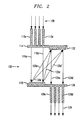
- FIG. 2 One such optical crossconnect 100 in accordance with a currently preferred embodiment of the invention is depicted in FIG. 2.
- Crossconnect 100 receives input optic signals 108 through a plurality of optic fibers 112, preferably formed in an array as is well known in the art.
- fiber array 112 is shown as a one-dimensional array having four fibers 112a, 112b, 112c, 112d. It is in any event to be understood that fiber array 112 as well as other fiber arrays discussed herein are preferably two-dimensional N x N arrays.
- Fiber array 112 transmits the optical signals 108 to an array of lenses 114 preferably functioning as collimating lenses.
- the lens array 114 is positioned relative to the fiber array 112 so that each lens communicates with a corresponding fiber for producing pencil beams 116 from the optic signals 108.
- beam 116a is produced from a signal carried by fiber 112a
- beam 116d is produced from a signal carried by fiber 112d, etc.
- a first MEMS tilt mirror array 118 also referred to as an input array, is positioned in alignment with the lens array 114 so that each mirror element 12 (FIG. 1) will receive a beam 116.
- the mirror elements are tilted, in a manner discussed in application Serial No. 09/415,178, to reflect the beams 116 to a second or output MEMS mirror array 122 positioned in optical communication with MEMS array 118.
- the reflected signals can be selectively directed to specific mirror elements in the output MEMS array 122.
- beam 116a is shown generating reflection beams 120a and 120a'
- beam 116d is shown generating reflection beams 120d and 120d'.
- beams are received by mirror elements in the output MEMS array 122 and are directed as beams 124 to an output lens array 126.
- An output fiber array 128 is aligned with the lens array 126 to receive and output optical signals 129.
- lens array 126 couples beams 124 into the output fiber array 128.
- the crossconnect device 100 contains a 1-to-1 mapping of each output fiber to a mirror in the output mirror array. This is required with single mode fibers because of the small numerical aperture which necessitates coaxial alignment of the input and output beams with the fiber axes to achieve low power loss.
- the crossconnect of FIG. 2 allows for adequate spacing of the fiber and mirror arrays to limit the required mirror angle excursions.
- a typical spacing dimension which will result in reduced diffraction losses is between 50-100 mm. If the mirror, lens and fiber arrays are coplanar, i.e. input fiber array 112, input lens 114 and output mirror array 122 are coplanar with each other, and output fiber array 128, output lens array 126 and input mirror array 118 are coplanar with each other, thus two similar monolithic blocks may be formed. Assembly of the crossconnect will then only require one six-axis alignment.
- crossconnect 200 contains an array of input lenses 214, and an array of output lenses 226 which communicate optical signals through an input fiber array 212 and an output fiber array 228, respectively.
- Input and output MEMS mirror arrays 218 and 222 are spaced apart from lens arrays 214, 226 for directing optical signals between the input fiber array and output fiber array.
- the device in FIG. 3 has the MEMS mirror arrays and lens arrays positioned on opposite sides of the crossconnect fabric, which allows for ease in construction.
- the mirror arrays can be monolithically integrated on a first common substrate and the lens arrays and fiber arrays monolithically integrated on a second common substrate.
- the lens arrays 214, 226 are formed on a common substrate and spaced apart from each other so that a reflective element 230 can be disposed therebetween.
- Reflective element 230 may be a separate plane mirror or, preferably, a reflective coating material (e.g. gold) deposited on the lens substrate and positioned for communicating optical signals between mirror array 218 and mirror array 222.
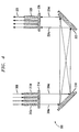
- FIG. 4 a variation of the crossconnect of FIG. 3 is shown as crossconnect 300.
- a primary difference from the embodiment of FIG. 3 is the removal of reflective element 230.
- mirror arrays 318 and 322 are angled relative to the substrate planes containing lens arrays 314 and 326 so that the optical signals can be communicated directly between the mirror arrays.
- the maximum distance between each fiber array (e.g., array 312) and its opposing mirror array (e.g., array 318) can be small. This is an important design consideration, especially if the pointing accuracy of the fiber array is poor.
- the mirror elements in the mirror arrays can be used not only to adjust the switch connects (e.g., a routing function) but also to compensate for imperfections in the fiber array.
- FIG. 5 depicts another crossconnect 400 which employs a plane mirror 430 in an offset configuration relative to a single MEMS mirror array 420.
- a single fiber array 410, single lens array 416 and single MEMS mirror array 420 are used in a "folded" crossconnect arrangement.
- the single fiber array functions as a combined input/output array.
- An input signal 412 is provided to lens array 416 by fiber 414 for imaging on a mirror element 420a.
- the beam is then reflected to plane mirror 430 and reflected back to mirror element 420b for output through lens array 416 to output fiber 422. It should be noted that in this configuration, there is no distinction between input and output ports.
- the crossconnect can be used as a 1 x 10²³ switch, an array of 341 1 x 2 switches, or a 512 x 512 optical crossconnect.
- Other variations of course exist, as do other mixtures of crossconnect components e.g. two 1 x 128 switches, sixty-four 2 x 2 switches and one 256 x 256 switches may be used with a 32 x 32 mirror array).
Landscapes
- Physics & Mathematics (AREA)
- General Physics & Mathematics (AREA)
- Optics & Photonics (AREA)
- Mechanical Light Control Or Optical Switches (AREA)
- Use Of Switch Circuits For Exchanges And Methods Of Control Of Multiplex Exchanges (AREA)
- Optical Communication System (AREA)
Abstract
Description
Claims (9)
- An optical crossconnect device for directing optical signals received from a plurality of input optic fibers to a plurality of output optic fibers, comprising:an array of lenses positioned for receiving the optical signals from the plurality of input optic fibers and for directing the optic signals; anda MEMS mirror array having a plurality of mirror elements, with each mirror element having a rotational axis about which each said mirror element is selectively operably tiltable, said mirror array being positioned for receiving optical signals directed by said lens array and for reflecting the directed optical signals to the plurality of output optic fibers.
- The device of claim 1, wherein said lens array receives the reflected optical signals from said MEMS mirror array and directs the reflected optical signals to the plurality of output optic fibers.
- The device of claim 1, wherein said each rotational axis comprises a first rotational axis and a second rotational axis and wherein said each mirror element is operatively tiltable relative to said first and second axes.
- The device of claim 1, wherein said MEMS mirror array comprises an input mirror array and an output mirror array, said output mirror array being disposed in optical communication with said input mirror array for receiving reflected optical signals from said input mirror array, and for directing the received, reflected optical signals to the plurality of output optic fibers.
- The device of claim 1, wherein said array of lenses comprises an input array of lenses for receiving optical signals from the plurality of input optic fibers, said device further comprising an output array of lenses in optical communication with said MEMS mirror array for directing the optical signals to the plurality of output optic fibers.
- The device of claim 4, wherein said array of lenses comprises an input array of lenses for receiving optical signals from the plurality of input optic fibers and for directing the received optical signals to said input mirror array, said device further comprising an output array of lenses in optical communication with said MEMS mirror array for receiving optical signals from said output mirror array and for directing the received optical signals to the plurality of output optic fibers.
- The device of claim 6, wherein said input array of lenses is coplanar with said output array of lenses.
- The device of claim 7, wherein said input and output arrays of lenses are formed on a common substrate and are distally displaced from each other to define an area therebetween, said device further comprising a reflecting element disposed on said area for receiving optical signals from said input mirror array and for directing optical signals to said output mirror array.
- The device of claim 1, wherein the plurality of input optic fibers and the plurality of output optic fibers form an array of optic fibers, said device further comprising a reflector element disposed in optical communication with said MEMS mirror array for receiving optical signals from said MEMS mirror array and for reflecting the received optical signals back to said MEMS mirror array, said reflected optical signals being redirected by said MEMS mirror array back to said array of lenses for receipt by the array of optic fibers.
Applications Claiming Priority (4)
| Application Number | Priority Date | Filing Date | Title |
|---|---|---|---|
| US16614999P | 1999-11-17 | 1999-11-17 | |
| US166149P | 1999-11-17 | ||
| US512174 | 2000-02-24 | ||
| US09/512,174 US6690885B1 (en) | 1999-10-07 | 2000-02-24 | Optical crossconnect using tilting mirror MEMS array |
Publications (3)
| Publication Number | Publication Date |
|---|---|
| EP1102096A2 true EP1102096A2 (en) | 2001-05-23 |
| EP1102096A3 EP1102096A3 (en) | 2002-07-10 |
| EP1102096B1 EP1102096B1 (en) | 2005-03-23 |
Family
ID=26862005
Family Applications (1)
| Application Number | Title | Priority Date | Filing Date |
|---|---|---|---|
| EP00309821A Expired - Lifetime EP1102096B1 (en) | 1999-11-17 | 2000-11-06 | Optical crossconnect using tilting mirror MEMS array |
Country Status (4)
| Country | Link |
|---|---|
| EP (1) | EP1102096B1 (en) |
| JP (2) | JP4619519B2 (en) |
| CA (1) | CA2325250A1 (en) |
| DE (1) | DE60018883T2 (en) |
Cited By (11)
| Publication number | Priority date | Publication date | Assignee | Title |
|---|---|---|---|---|
| WO2001079900A3 (en) * | 2000-04-14 | 2002-05-16 | Cspeed Corp | Fiber optic cross connect with folding of light beams |
| EP1113302A3 (en) * | 1999-12-01 | 2002-08-21 | Lucent Technologies Inc. | Folded optical cross connect with a curved mirror |
| EP1271202A1 (en) * | 2001-06-29 | 2003-01-02 | Lucent Technologies Inc. | Optical MEMS switch with imaging system |
| EP1271200A1 (en) * | 2001-06-29 | 2003-01-02 | Lucent Technologies Inc. | Imaging technique and optical switch using optical MEMS devices |
| WO2002021190A3 (en) * | 2000-09-08 | 2003-01-09 | Harris Corp | Fiber optic switch and associated methods |
| US6543087B2 (en) | 2001-06-01 | 2003-04-08 | Aip Networks, Inc. | Micro-electromechanical hinged flap structure |
| EP1397713A2 (en) * | 2001-06-18 | 2004-03-17 | Raytheon Company | Method and apparatus for integrating optical fibers with collimating lenses |
| EP1099966A3 (en) * | 1999-11-09 | 2004-08-18 | Texas Instruments Incorporated | Micromirror optical switch |
| US6941034B2 (en) | 2002-06-25 | 2005-09-06 | Olympus Corporation | Optical switch and adjustment method thereof |
| US9304259B1 (en) | 2014-03-13 | 2016-04-05 | Google Inc. | MEMS mirror arrays having multiple mirror units |
| GB2563476A (en) * | 2017-06-15 | 2018-12-19 | Google Llc | Inner and outer collimator elements for an optical circuit switch |
Families Citing this family (12)
| Publication number | Priority date | Publication date | Assignee | Title |
|---|---|---|---|---|
| JP4745579B2 (en) * | 1999-12-01 | 2011-08-10 | エクスロス インコーポレイテッド ノーテル ネットワークス | Multiple 1 × N optical switch configuration |
| US7050669B2 (en) * | 2001-04-30 | 2006-05-23 | Trex Enterprises Corp. | Optical cross connect switch with axial alignment beam |
| JP2003066348A (en) | 2001-08-28 | 2003-03-05 | Nec Corp | Optical transmission system |
| JP3908503B2 (en) * | 2001-10-30 | 2007-04-25 | 富士通株式会社 | Light switch |
| CN100395579C (en) | 2002-01-29 | 2008-06-18 | 松下电器产业株式会社 | Deformable mirror and control device with the deformable mirror |
| JP2004037791A (en) * | 2002-07-03 | 2004-02-05 | Olympus Corp | Electrostatic drive type mirror arrangement |
| WO2005011322A2 (en) | 2003-07-28 | 2005-02-03 | Olympus Corporation | Optical switch and method of controlling optical switch |
| JP4489393B2 (en) | 2003-08-21 | 2010-06-23 | オリンパス株式会社 | Semiconductor device |
| JP4592292B2 (en) | 2004-01-16 | 2010-12-01 | 株式会社日本マイクロニクス | Electrical connection device |
| JP4813061B2 (en) | 2005-01-19 | 2011-11-09 | オリンパス株式会社 | Light switch |
| JP4556879B2 (en) | 2005-03-31 | 2010-10-06 | 日立金属株式会社 | Optical switch and optical switch array |
| US9664896B1 (en) | 2014-03-13 | 2017-05-30 | Google Inc. | Pre-tilted MEMS mirrors |
Family Cites Families (6)
| Publication number | Priority date | Publication date | Assignee | Title |
|---|---|---|---|---|
| US5037173A (en) * | 1989-11-22 | 1991-08-06 | Texas Instruments Incorporated | Optical interconnection network |
| JP2617054B2 (en) * | 1991-10-18 | 1997-06-04 | 日本電信電話株式会社 | Optical connection module |
| US5444801A (en) * | 1994-05-27 | 1995-08-22 | Laughlin; Richard H. | Apparatus for switching optical signals and method of operation |
| IL140031A0 (en) * | 1998-06-05 | 2002-02-10 | Astarte Fiber Networks Inc | Planar array optical switch and method |
| JP2000019434A (en) * | 1998-06-30 | 2000-01-21 | Nippon Signal Co Ltd:The | Optical selector |
| EP1121616A2 (en) * | 1998-09-15 | 2001-08-08 | Xros, Inc. | Flexible, modular, compact fiber optic switch |
-
2000
- 2000-11-06 EP EP00309821A patent/EP1102096B1/en not_active Expired - Lifetime
- 2000-11-06 DE DE60018883T patent/DE60018883T2/en not_active Expired - Lifetime
- 2000-11-08 CA CA002325250A patent/CA2325250A1/en not_active Abandoned
- 2000-11-17 JP JP2000350490A patent/JP4619519B2/en not_active Expired - Fee Related
-
2010
- 2010-01-12 JP JP2010003906A patent/JP2010134472A/en active Pending
Cited By (17)
| Publication number | Priority date | Publication date | Assignee | Title |
|---|---|---|---|---|
| EP1099966A3 (en) * | 1999-11-09 | 2004-08-18 | Texas Instruments Incorporated | Micromirror optical switch |
| EP1113302A3 (en) * | 1999-12-01 | 2002-08-21 | Lucent Technologies Inc. | Folded optical cross connect with a curved mirror |
| WO2001079900A3 (en) * | 2000-04-14 | 2002-05-16 | Cspeed Corp | Fiber optic cross connect with folding of light beams |
| US6556740B1 (en) | 2000-04-14 | 2003-04-29 | Nanogear | Fiber optic cross connect with folding of light beams |
| WO2002021190A3 (en) * | 2000-09-08 | 2003-01-09 | Harris Corp | Fiber optic switch and associated methods |
| US6543087B2 (en) | 2001-06-01 | 2003-04-08 | Aip Networks, Inc. | Micro-electromechanical hinged flap structure |
| EP1397713A2 (en) * | 2001-06-18 | 2004-03-17 | Raytheon Company | Method and apparatus for integrating optical fibers with collimating lenses |
| US6704476B2 (en) | 2001-06-29 | 2004-03-09 | Lucent Technologies Inc. | Optical MEMS switch with imaging system |
| US6647172B2 (en) | 2001-06-29 | 2003-11-11 | Lucent Technologies Inc. | Imaging technique for use with optical MEMS devices |
| EP1271200A1 (en) * | 2001-06-29 | 2003-01-02 | Lucent Technologies Inc. | Imaging technique and optical switch using optical MEMS devices |
| EP1271202A1 (en) * | 2001-06-29 | 2003-01-02 | Lucent Technologies Inc. | Optical MEMS switch with imaging system |
| US6941034B2 (en) | 2002-06-25 | 2005-09-06 | Olympus Corporation | Optical switch and adjustment method thereof |
| US9304259B1 (en) | 2014-03-13 | 2016-04-05 | Google Inc. | MEMS mirror arrays having multiple mirror units |
| US9625652B1 (en) | 2014-03-13 | 2017-04-18 | Google Inc. | MEMS mirror arrays having multiple mirror units |
| GB2563476A (en) * | 2017-06-15 | 2018-12-19 | Google Llc | Inner and outer collimator elements for an optical circuit switch |
| US10317626B2 (en) | 2017-06-15 | 2019-06-11 | Google Llc | Inner and outer collimator elements for an optical circuit switch |
| GB2563476B (en) * | 2017-06-15 | 2020-07-01 | Google Llc | Inner and outer collimator elements for an optical circuit switch |
Also Published As
| Publication number | Publication date |
|---|---|
| EP1102096B1 (en) | 2005-03-23 |
| CA2325250A1 (en) | 2001-05-17 |
| EP1102096A3 (en) | 2002-07-10 |
| JP2001174724A (en) | 2001-06-29 |
| JP2010134472A (en) | 2010-06-17 |
| DE60018883T2 (en) | 2006-04-13 |
| DE60018883D1 (en) | 2005-04-28 |
| JP4619519B2 (en) | 2011-01-26 |
Similar Documents
| Publication | Publication Date | Title |
|---|---|---|
| US6690885B1 (en) | Optical crossconnect using tilting mirror MEMS array | |
| EP1102096B1 (en) | Optical crossconnect using tilting mirror MEMS array | |
| EP1099970B1 (en) | Method and device for optically crossconnecting optical signals using tilting mirror mems with drift monitoring feature | |
| US5943454A (en) | Freespace optical bypass-exchange switch | |
| US6975789B2 (en) | Wavelength router | |
| CA2694309C (en) | Multiple function digital optical switch | |
| US6525863B1 (en) | Multi-technology multi-beam-former platform for robust fiber-optical beam control modules | |
| JPH11231232A (en) | Free space optical signal switching device | |
| US6760501B2 (en) | Device for imposing a field tilt for approximating the inherent field curvature of a focusing element in a free space optical device | |
| JP2004501395A (en) | Reconfigurable optical switch | |
| US20050088339A1 (en) | White cell antenna beamformers | |
| US6842556B2 (en) | Two input, two output optical switch using two movable mirrors | |
| US20020061161A1 (en) | Optical switch | |
| US6798951B2 (en) | Wavelength router with a transmissive dispersive element | |
| US20030118276A1 (en) | Optical switch having a retro-reflector associated therewith and a method of use thereof | |
| US20030202739A1 (en) | Optical switch unit and a method therefore | |
| CA2363625A1 (en) | Optical switch |
Legal Events
| Date | Code | Title | Description |
|---|---|---|---|
| PUAI | Public reference made under article 153(3) epc to a published international application that has entered the european phase |
Free format text: ORIGINAL CODE: 0009012 |
|
| AK | Designated contracting states |
Kind code of ref document: A2 Designated state(s): AT BE CH CY DE DK ES FI FR GB GR IE IT LI LU MC NL PT SE TR |
|
| AX | Request for extension of the european patent |
Free format text: AL;LT;LV;MK;RO;SI |
|
| PUAL | Search report despatched |
Free format text: ORIGINAL CODE: 0009013 |
|
| AK | Designated contracting states |
Kind code of ref document: A3 Designated state(s): AT BE CH CY DE DK ES FI FR GB GR IE IT LI LU MC NL PT SE TR |
|
| AX | Request for extension of the european patent |
Free format text: AL;LT;LV;MK;RO;SI |
|
| 17P | Request for examination filed |
Effective date: 20030107 |
|
| AKX | Designation fees paid |
Designated state(s): DE FR GB |
|
| 17Q | First examination report despatched |
Effective date: 20030224 |
|
| GRAP | Despatch of communication of intention to grant a patent |
Free format text: ORIGINAL CODE: EPIDOSNIGR1 |
|
| GRAS | Grant fee paid |
Free format text: ORIGINAL CODE: EPIDOSNIGR3 |
|
| GRAA | (expected) grant |
Free format text: ORIGINAL CODE: 0009210 |
|
| AK | Designated contracting states |
Kind code of ref document: B1 Designated state(s): DE FR GB |
|
| REG | Reference to a national code |
Ref country code: GB Ref legal event code: FG4D |
|
| REG | Reference to a national code |
Ref country code: IE Ref legal event code: FG4D |
|
| REF | Corresponds to: |
Ref document number: 60018883 Country of ref document: DE Date of ref document: 20050428 Kind code of ref document: P |
|
| PLBE | No opposition filed within time limit |
Free format text: ORIGINAL CODE: 0009261 |
|
| STAA | Information on the status of an ep patent application or granted ep patent |
Free format text: STATUS: NO OPPOSITION FILED WITHIN TIME LIMIT |
|
| ET | Fr: translation filed | ||
| 26N | No opposition filed |
Effective date: 20051227 |
|
| REG | Reference to a national code |
Ref country code: GB Ref legal event code: 732E Free format text: REGISTERED BETWEEN 20131107 AND 20131113 |
|
| REG | Reference to a national code |
Ref country code: FR Ref legal event code: CD Owner name: ALCATEL-LUCENT USA INC. Effective date: 20131122 |
|
| REG | Reference to a national code |
Ref country code: FR Ref legal event code: GC Effective date: 20140410 |
|
| REG | Reference to a national code |
Ref country code: FR Ref legal event code: RG Effective date: 20141015 |
|
| REG | Reference to a national code |
Ref country code: FR Ref legal event code: PLFP Year of fee payment: 16 |
|
| REG | Reference to a national code |
Ref country code: FR Ref legal event code: PLFP Year of fee payment: 17 |
|
| REG | Reference to a national code |
Ref country code: FR Ref legal event code: PLFP Year of fee payment: 18 |
|
| PGFP | Annual fee paid to national office [announced via postgrant information from national office to epo] |
Ref country code: FR Payment date: 20171020 Year of fee payment: 18 |
|
| PGFP | Annual fee paid to national office [announced via postgrant information from national office to epo] |
Ref country code: GB Payment date: 20171020 Year of fee payment: 18 |
|
| GBPC | Gb: european patent ceased through non-payment of renewal fee |
Effective date: 20181106 |
|
| PG25 | Lapsed in a contracting state [announced via postgrant information from national office to epo] |
Ref country code: FR Free format text: LAPSE BECAUSE OF NON-PAYMENT OF DUE FEES Effective date: 20181130 |
|
| PG25 | Lapsed in a contracting state [announced via postgrant information from national office to epo] |
Ref country code: GB Free format text: LAPSE BECAUSE OF NON-PAYMENT OF DUE FEES Effective date: 20181106 |
|
| PGFP | Annual fee paid to national office [announced via postgrant information from national office to epo] |
Ref country code: DE Payment date: 20191127 Year of fee payment: 20 |
|
| REG | Reference to a national code |
Ref country code: DE Ref legal event code: R071 Ref document number: 60018883 Country of ref document: DE |