EP1101260B1 - Controlling laser polarization - Google Patents
Controlling laser polarization Download PDFInfo
- Publication number
- EP1101260B1 EP1101260B1 EP99930474A EP99930474A EP1101260B1 EP 1101260 B1 EP1101260 B1 EP 1101260B1 EP 99930474 A EP99930474 A EP 99930474A EP 99930474 A EP99930474 A EP 99930474A EP 1101260 B1 EP1101260 B1 EP 1101260B1
- Authority
- EP
- European Patent Office
- Prior art keywords
- polarization
- laser
- link
- laser beam
- links
- Prior art date
- Legal status (The legal status is an assumption and is not a legal conclusion. Google has not performed a legal analysis and makes no representation as to the accuracy of the status listed.)
- Expired - Lifetime
Links
Images


Classifications
-
- H—ELECTRICITY
- H01—ELECTRIC ELEMENTS
- H01S—DEVICES USING THE PROCESS OF LIGHT AMPLIFICATION BY STIMULATED EMISSION OF RADIATION [LASER] TO AMPLIFY OR GENERATE LIGHT; DEVICES USING STIMULATED EMISSION OF ELECTROMAGNETIC RADIATION IN WAVE RANGES OTHER THAN OPTICAL
- H01S3/00—Lasers, i.e. devices using stimulated emission of electromagnetic radiation in the infrared, visible or ultraviolet wave range
- H01S3/10—Controlling the intensity, frequency, phase, polarisation or direction of the emitted radiation, e.g. switching, gating, modulating or demodulating
- H01S3/11—Mode locking; Q-switching; Other giant-pulse techniques, e.g. cavity dumping
- H01S3/1123—Q-switching
- H01S3/115—Q-switching using intracavity electro-optic devices
-
- B—PERFORMING OPERATIONS; TRANSPORTING
- B23—MACHINE TOOLS; METAL-WORKING NOT OTHERWISE PROVIDED FOR
- B23K—SOLDERING OR UNSOLDERING; WELDING; CLADDING OR PLATING BY SOLDERING OR WELDING; CUTTING BY APPLYING HEAT LOCALLY, e.g. FLAME CUTTING; WORKING BY LASER BEAM
- B23K26/00—Working by laser beam, e.g. welding, cutting or boring
- B23K26/02—Positioning or observing the workpiece, e.g. with respect to the point of impact; Aligning, aiming or focusing the laser beam
- B23K26/06—Shaping the laser beam, e.g. by masks or multi-focusing
- B23K26/073—Shaping the laser spot
- B23K26/0736—Shaping the laser spot into an oval shape, e.g. elliptic shape
-
- B—PERFORMING OPERATIONS; TRANSPORTING
- B23—MACHINE TOOLS; METAL-WORKING NOT OTHERWISE PROVIDED FOR
- B23K—SOLDERING OR UNSOLDERING; WELDING; CLADDING OR PLATING BY SOLDERING OR WELDING; CUTTING BY APPLYING HEAT LOCALLY, e.g. FLAME CUTTING; WORKING BY LASER BEAM
- B23K26/00—Working by laser beam, e.g. welding, cutting or boring
- B23K26/02—Positioning or observing the workpiece, e.g. with respect to the point of impact; Aligning, aiming or focusing the laser beam
- B23K26/06—Shaping the laser beam, e.g. by masks or multi-focusing
- B23K26/062—Shaping the laser beam, e.g. by masks or multi-focusing by direct control of the laser beam
- B23K26/0622—Shaping the laser beam, e.g. by masks or multi-focusing by direct control of the laser beam by shaping pulses
- B23K26/0624—Shaping the laser beam, e.g. by masks or multi-focusing by direct control of the laser beam by shaping pulses using ultrashort pulses, i.e. pulses of 1 ns or less
-
- B—PERFORMING OPERATIONS; TRANSPORTING
- B23—MACHINE TOOLS; METAL-WORKING NOT OTHERWISE PROVIDED FOR
- B23K—SOLDERING OR UNSOLDERING; WELDING; CLADDING OR PLATING BY SOLDERING OR WELDING; CUTTING BY APPLYING HEAT LOCALLY, e.g. FLAME CUTTING; WORKING BY LASER BEAM
- B23K26/00—Working by laser beam, e.g. welding, cutting or boring
- B23K26/02—Positioning or observing the workpiece, e.g. with respect to the point of impact; Aligning, aiming or focusing the laser beam
- B23K26/06—Shaping the laser beam, e.g. by masks or multi-focusing
- B23K26/064—Shaping the laser beam, e.g. by masks or multi-focusing by means of optical elements, e.g. lenses, mirrors or prisms
- B23K26/0643—Shaping the laser beam, e.g. by masks or multi-focusing by means of optical elements, e.g. lenses, mirrors or prisms comprising mirrors
-
- B—PERFORMING OPERATIONS; TRANSPORTING
- B23—MACHINE TOOLS; METAL-WORKING NOT OTHERWISE PROVIDED FOR
- B23K—SOLDERING OR UNSOLDERING; WELDING; CLADDING OR PLATING BY SOLDERING OR WELDING; CUTTING BY APPLYING HEAT LOCALLY, e.g. FLAME CUTTING; WORKING BY LASER BEAM
- B23K26/00—Working by laser beam, e.g. welding, cutting or boring
- B23K26/02—Positioning or observing the workpiece, e.g. with respect to the point of impact; Aligning, aiming or focusing the laser beam
- B23K26/06—Shaping the laser beam, e.g. by masks or multi-focusing
- B23K26/0665—Shaping the laser beam, e.g. by masks or multi-focusing by beam condensation on the workpiece, e.g. for focusing
-
- B—PERFORMING OPERATIONS; TRANSPORTING
- B23—MACHINE TOOLS; METAL-WORKING NOT OTHERWISE PROVIDED FOR
- B23K—SOLDERING OR UNSOLDERING; WELDING; CLADDING OR PLATING BY SOLDERING OR WELDING; CUTTING BY APPLYING HEAT LOCALLY, e.g. FLAME CUTTING; WORKING BY LASER BEAM
- B23K2101/00—Articles made by soldering, welding or cutting
- B23K2101/36—Electric or electronic devices
- B23K2101/38—Conductors
-
- B—PERFORMING OPERATIONS; TRANSPORTING
- B23—MACHINE TOOLS; METAL-WORKING NOT OTHERWISE PROVIDED FOR
- B23K—SOLDERING OR UNSOLDERING; WELDING; CLADDING OR PLATING BY SOLDERING OR WELDING; CUTTING BY APPLYING HEAT LOCALLY, e.g. FLAME CUTTING; WORKING BY LASER BEAM
- B23K2103/00—Materials to be soldered, welded or cut
- B23K2103/08—Non-ferrous metals or alloys
- B23K2103/12—Copper or alloys thereof
Definitions
- the present invention relates in general to laser processing of workpieces such as semiconductor devices and more particularly concerns processing of DRAMS, memories, and programmable devices by cutting fuses or links.
- Recent semiconductor devices have link geometries typically about 1 ⁇ m wide by 5 ⁇ m long. These links may be located in groups of horizontally aligned links and vertically aligned links. A laser having 3-5 ⁇ m laser spot size may be used to disconnect such a link using a single laser pulse. By appropriately selecting the laser energy, the spot size, the laser pulse width, and the wavelength of the laser beam, it is possible to optimize laser parameters in order to achieve the cleanest and most reliable link disconnect.
- the quality of a link disconnect may be evaluated by visually inspecting the blasted link.
- One measure of practicality in fuse or link disconnect is the energy cutting range or "energy window,” which is the range of energies per pulse over which clean and reliable link cutting can be achieved.
- the laser energy that is used to process a semiconductor device can be set at the center of the predicted energy window, which may differ somewhat from the actual energy window due to process variations such as the thickness of the link material, the thickness of oxide material located on top of the link, laser instability, errors in the positioning of the laser beam, and focusing errors.
- US-A-4 908 493 describes rotating the plane of polarization of a linearly polarized laser beam in relation to a work piece of a material being processed simultaneously and in synchronization with steering the laser beam over the work piece so as to keep the plane of polarization parallel to either the plane of incidence or the direction of travel of the beam in relation to the work piece. Also, depending to some extent on the particular processing being accomplished, such as welding fusing, the angle of incidence of the laser beam on the work piece is kept at or near the polarizing or Brewster's angle.
- US-A-5 185 753 describes an unstable resonator system which is controlled in polarization by the use of a compound resonator in which the parent resonator is coupled to a polarization control leg by an aperture that passes a small portion of the output beam into a polarization control element and returns a polarized feedback beam mode-matched to the adjoint mode of the parent resonator.
- One aspect of the invention features a laser polarization control apparatus that includes a polarization modifying device, such as a liquid crystal variable retarder, and a controller.
- the polarization modifying device receives a laser beam and modifies the polarization of the laser beam.
- the controller which is connected to the polarization modifying device, adjusts an input to the polarization modifying device in order to control modification of the polarization of the laser beam based on alignment of a structure to be processed by the laser beam. For example, the polarization of the laser beam may be rotated to correspond with the alignment of a link in a semiconductor device to be cut by the laser beam.
- the polarization modifying device is configured for incorporation into a laser processing system that produces the laser beam received by the polarization modifying device and that focuses the laser beam modified by the polarization modifying device onto a workpiece that includes the structure to be processed by the laser beam.
- a linearly or elliptically polarized laser beam may be aligned with a link to be cut.
- the polarization of the laser beam may be vertically aligned when the link is aligned vertically and is horizontally aligned when the link is aligned horizontally.
- An analyzer tool receives the laser beam modified by the polarization modification device.
- the analyzer tool measures the modification of the polarization of the laser beam by the polarization modification device.
- a plurality of inputs are applied to the polarization modifying device to control modification of the polarization of the laser beam, and the laser beam modified by the polarization modification device is analyzed using the analyzer tool in order to measure modification of the polarization of the laser beam by the polarization modification device.
- the relationship between the inputs to the polarization control device and the modification of the polarization of the laser beam is stored.
- the polarization modification device may modify polarization of the laser beam based on this stored relationship.
- the polarization modification device By applying a variety of inputs to the polarization modification device and by analyzing the laser beam modified by the polarization modification device, it is possible to identify the appropriate inputs required to obtain vertical linear polarization and horizontal linear polarization, for example. These inputs can then be stored for later use when the laser system processes links on a semiconductor device, so that the appropriate inputs can be applied to the polarization modification device to ensure that the polarization of the laser beam will be vertically aligned when the link is aligned vertically and horizontally aligned when the link is aligned horizontally.
- a linearly or elliptically polarized laser beam is aligned with a link to be cut in order to increase the energy window of a laser processing system.
- the invention provides a broad range of energies over which a given link can be cut well, the invention increases the likelihood of successful disconnection of the link despite known or unknown process parameters that tend to affect the processing of the link and therefore affect the optimal cutting energy.
- process parameters can include, for example, the uncertainty in the thickness of an oxide layer over the link material, slight misalignments of the link with the laser beam due to positioning errors, instability of the laser pulse or of the laser pulse energy, focus errors, and uncertainty as to the thickness of the link.
- the laser energy that is to be used to cut the link is set based on an experimental determination of the center of the predicted energy window for the particular type of link.
- certain semiconductor wafers may have a thick oxide layer while others may have a thin oxide layer or no oxide layer.
- the customer may perform an experimental energy study on different types of wafers in order to determine the predicted energy window for a thin wafer and the predicted energy window for a thicker wafer, which will typically cover a higher energy range.
- there could be various different types of links that require different energies to be optically cut.
- At the edges of the wafer for example, there may be processing considerations from which it is experimentally determined that the center of the predicted energy window should be different as compared with other regions of the wafer.
- the invention provides a wide range of energies that are effective for cutting a given link, the preselected laser energy is likely to fall within this wide range for the given link, because the actual energy window is very likely to overlap the preselected laser energy. For this reason, the large energy cutting range provided by the invention is very useful for maintaining reliable link cutting.
- the invention utilizes a linearly or elliptically polarized laser beam rather than a circularly polarized laser beam, it is possible to align the polarization of the laser beam with the link and thereby optimize the actual energy window.
- the actual energy window may, at least under certain circumstances, be larger than it would be if the same laser beam were linearly or elliptically polarized and aligned perpendicularly to the link.
- certain laser systems can allow the user to select a circularly polarized laser beam as a compromise option if the user does not wish to go through the process of ensuring that a linearly or elliptically polarized laser beam is aligned with the link. It is believed that the largest energy windows can be achieved by aligning a linearly polarized beam with the link to be cut.
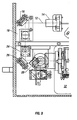
- FIGS. 1 and 2 show the major components of a laser system 10 according to the invention, prior to installation of a liquid crystal variable retarder and a polarizing beamsplitter that are used to adjust linear polarization based on the alignment of a link to be cut.
- Diode-pumped Q-switched laser head 20 produces a laser beam 12, shown by a dashed line, that passes through halfwave plate 22 (see the detail shown in FIG. 4) that causes the laser beam to be linearly polarized.
- Laser beam 12 proceeds through small pre-expander telescope assembly 14, which may, for example, expand the laser beam about three times, and then laser beam 12 reflects off of rear turning mirror 16, taking a 90-degree turn.
- Laser beam 12 reflects off of front turning mirror 26 and proceeds through beamsplitter 28 and telescope assembly 32 toward scan lens 30, which includes galvanometers 34 and 36 that direct laser beam 12 toward a work surface.
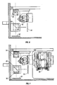
- FIG. 3 which shows the laser system 10 of FIGS. 1 and 2 after installation of a liquid crystal variable retarder 24 and a polarizing beamsplitter 18, after laser beam 12 reflects off of rear turning mirror 16, it proceeds through polarizing beamsplitter assembly 18, which dumps a portion of the energy of the laser beam (in order to obtain stable, short pulses, the laser may be operated at maximum power, with the laser rod being pumped as hard as possible).
- Polarizing beamsplitter assembly 18 dumps the horizontally polarized portion of laser beam 12 and allows vertically polarized portions of laser beam 12 to be transmitted through it.
- Laser beam 12 itself is linearly polarized prior to entering polarizing beamsplitter assembly 18, and so by rotating half wave plate 22 it is possible to control the percentage of laser beam 12 that is dumped by polarizing beamsplitter assembly 18, so that polarizing beamsplitter assembly 18 in effect functions as a variable beamsplitter. Laser beam 12 coming out of polarizing beamsplitter assembly 18 is always vertically polarized.
- the birefringent liquid crystal can rotate the polarization of a laser beam, because light moves at different speeds along different axes through the birefringent liquid crystal, resulting in a phase shift of the polarization.
- the birefringent liquid crystal can also transform the linearly polarized laser input into an elliptically or circularly polarized laser output.
- Laser beam 12 maintains its polarization as it travels from LCVR 24 to the work surface. No other optics external to laser system 10 are required in order to change the polarization of laser beam 12.
- the voltage applied to liquid crystal variable retarder 24 is controlled by a digital controller 44 and/or a manual controller 40, which interface with liquid crystal variable retarder 24 through a cable that passes through a cable port of the laser system shown in FIG. 1.
- Manual controller 40 can be adjusted by a user in order to vary the voltage to LCVR 24, based on the user's knowledge of whether a link to be destroyed is vertical or horizontal, for example.
- Digital controller 44 receives input from computer 42 in order to automatically vary the voltage to LCVR 24 based on information stored in computer 42 pertaining to the alignment of the links to be cut. This input from computer 42 controls digital controller 44 so as to cause an appropriate voltage to be applied to LCVR 24.
- digital controller 44 is programmed to select among three different voltages corresponding to vertical linear polarization, horizontal linear polarization, and circular polarization.
- digital controller 44 stores sixty-four or ninety-six different voltages, including voltages corresponding to various elliptical polarizations.
- the liquid crystal variable retarder is capable of rotating linear polarization to numerous angles other than the vertical or the horizontal, in the event that polarization at such angles proves useful for cutting certain types of structures.
- Polarizing beamsplitter analyzer tool 46 which is used to analyze the polarization of laser beam 12 after it passes through LCVR 24, includes polarizing beamsplitter 48 having a quarter wave plate 50 positioned in front of it.
- Quarter wave plate 50 linearizes any circularly polarized light received from LCVR 24, so that when this circularly polarized light goes to the polarizing beamsplitter it will be 100 percent transmitted or 100 percent reflected depending on its handedness.
- Detection plates 52 and 54 detect the amount of light that is transmitted through polarizing beamsplitter 48 and the amount of light reflected by polarizing beamsplitter 48, respectively. If the light received from LCVR 24 is not circularly polarized, however, but is instead elliptically polarized, then less than 100 percent of the light received from LCVR 24 will be transmitted or reflected. In this manner it is possible to determine whether a voltage that is applied to LCVR 24 is appropriate for yielding circular polarization.
- the orientation of beamsplitter analyzer tool 46 is flipped so that polarizing beamsplitter 48 is positioned in front of, rather than behind, quarter wave plate 50.
- quarter wave plate 50 does not perform any useful function because it simply converts linearly polarized light into circularly polarized light without changing the energy of the light that passes through it. If laser beam 12 is linearly polarized it should either be 100 percent transmitted through polarizing beamsplitter 48 or 100 percent reflected by polarizing beamsplitter 48, depending on whether laser beam 12 is vertically or horizontally polarized.
- a customer may program digital controller 44 to cause any arbitrary voltage to be applied to LCVR 24. For example, if a particular customer desires to identify a voltage that yields vertical elliptical polarization or horizontal elliptical polarization, the customer can find this voltage experimentally using the techniques described above in connection with FIGS. 6 and 7.
- the techniques described in connection with FIGS. 6 and 7 should be performed on an apparatus-by-apparatus basis because there may be some variation in the operation of LCVR 24 on an apparatus-by-apparatus basis and because different lasers may operate at different wavelengths, different voltages, and different polarizations. Thus, for example, if it were desired change the wavelength at which a particular laser system operates, it would be important to perform the experimentation procedures described above again.
- the laser system can be used to cut every other link in a bank of links (which may include thousands of links), with the polarization of the laser beam being aligned with each link, and with each link being cut at a slightly different energy.
- the links are then inspected to determine whether the links are cut cleanly, or whether the cut is ragged or material is blown out of the cutting area due to laser energy not being cleanly absorbed by the link. If the laser energy is too low the link will not be disconnected cleanly and if its much too low the link will not be disconnected at all. If the laser energy is too high, damage may occur to the substrate surrounding the link and to surrounding features such as other links.
- the links that are cleanly cut define the energy window.
Landscapes
- Physics & Mathematics (AREA)
- Optics & Photonics (AREA)
- Engineering & Computer Science (AREA)
- Plasma & Fusion (AREA)
- Mechanical Engineering (AREA)
- Electromagnetism (AREA)
- Laser Beam Processing (AREA)
- Lasers (AREA)
- Liquid Crystal (AREA)
Description
- The present invention relates in general to laser processing of workpieces such as semiconductor devices and more particularly concerns processing of DRAMS, memories, and programmable devices by cutting fuses or links.
- Laser systems have been used for many years in the fabrication of DRAMS and programmable devices. In DRAM production, for example, redundant memory is programmed by using a focused laser beam to cut fuses or links in the memory in order to replace defective memory cells. The programming is accomplished by disconnecting the fuses or links using a laser pulse generated by a diode pumped Q-switched YAG (or YLF) laser.
- Recent semiconductor devices have link geometries typically about 1 µm wide by 5 µm long. These links may be located in groups of horizontally aligned links and vertically aligned links. A laser having 3-5 µm laser spot size may be used to disconnect such a link using a single laser pulse. By appropriately selecting the laser energy, the spot size, the laser pulse width, and the wavelength of the laser beam, it is possible to optimize laser parameters in order to achieve the cleanest and most reliable link disconnect.
- The quality of a link disconnect may be evaluated by visually inspecting the blasted link. One measure of practicality in fuse or link disconnect is the energy cutting range or "energy window," which is the range of energies per pulse over which clean and reliable link cutting can be achieved. The laser energy that is used to process a semiconductor device can be set at the center of the predicted energy window, which may differ somewhat from the actual energy window due to process variations such as the thickness of the link material, the thickness of oxide material located on top of the link, laser instability, errors in the positioning of the laser beam, and focusing errors.
- Many diode-pumped solid-state lasers used in laser processing systems are linearly polarized. Certain laser processing systems use circularly polarized laser beams rather than linear polarized laser beams.
- US-A-4 908 493 describes rotating the plane of polarization of a linearly polarized laser beam in relation to a work piece of a material being processed simultaneously and in synchronization with steering the laser beam over the work piece so as to keep the plane of polarization parallel to either the plane of incidence or the direction of travel of the beam in relation to the work piece. Also, depending to some extent on the particular processing being accomplished, such as welding fusing, the angle of incidence of the laser beam on the work piece is kept at or near the polarizing or Brewster's angle.
- US-A-5 185 753 describes an unstable resonator system which is controlled in polarization by the use of a compound resonator in which the parent resonator is coupled to a polarization control leg by an aperture that passes a small portion of the output beam into a polarization control element and returns a polarized feedback beam mode-matched to the adjoint mode of the parent resonator.
- The present invention is defined in the attached independent claim, to which reference should now be made. Further, preferred features may be found in the sub-claims appended thereto.
- The invention is defined by the claims.
- One aspect of the invention features a laser polarization control apparatus that includes a polarization modifying device, such as a liquid crystal variable retarder, and a controller. The polarization modifying device receives a laser beam and modifies the polarization of the laser beam. The controller, which is connected to the polarization modifying device, adjusts an input to the polarization modifying device in order to control modification of the polarization of the laser beam based on alignment of a structure to be processed by the laser beam. For example, the polarization of the laser beam may be rotated to correspond with the alignment of a link in a semiconductor device to be cut by the laser beam. The polarization modifying device is configured for incorporation into a laser processing system that produces the laser beam received by the polarization modifying device and that focuses the laser beam modified by the polarization modifying device onto a workpiece that includes the structure to be processed by the laser beam.
- Thus, according to the invention, a linearly or elliptically polarized laser beam may be aligned with a link to be cut. For example, the polarization of the laser beam may be vertically aligned when the link is aligned vertically and is horizontally aligned when the link is aligned horizontally. It has been discovered that by utilizing this technique it is possible to increase the range of acceptable cutting energies that are effective for cutting certain types of links. This range of acceptable cutting energies is the energy window. Thus, by switching the polarization of the laser beam depending on the link orientation, the best results are obtained in terms of maximizing the width of the energy window. There may also be certain types of links for which the energy window is maximized when a linearly polarized laser beam is aligned perpendicularly to the link, or at some other angle, rather than parallel to the link.
- An analyzer tool receives the laser beam modified by the polarization modification device. The analyzer tool measures the modification of the polarization of the laser beam by the polarization modification device. A plurality of inputs are applied to the polarization modifying device to control modification of the polarization of the laser beam, and the laser beam modified by the polarization modification device is analyzed using the analyzer tool in order to measure modification of the polarization of the laser beam by the polarization modification device. The relationship between the inputs to the polarization control device and the modification of the polarization of the laser beam is stored. When the laser system is used to process a structure, the polarization modification device may modify polarization of the laser beam based on this stored relationship.
- By applying a variety of inputs to the polarization modification device and by analyzing the laser beam modified by the polarization modification device, it is possible to identify the appropriate inputs required to obtain vertical linear polarization and horizontal linear polarization, for example. These inputs can then be stored for later use when the laser system processes links on a semiconductor device, so that the appropriate inputs can be applied to the polarization modification device to ensure that the polarization of the laser beam will be vertically aligned when the link is aligned vertically and horizontally aligned when the link is aligned horizontally.
- Numerous other features, objects, and advantages of the invention will become apparent from the following detailed description when read in connection with the accompanying drawings.
-
- FIG. 1 is a horizontal cross-sectional view of a laser system according to the invention prior to installation of a liquid crystal variable retarder and a polarizing beamsplitter.
- FIG. 2 is a vertical cross-sectional view of the laser system of FIG. 1 taken along line 2-2 in FIG. 1.
- FIG. 3 is a horizontal cross-sectional view of a portion of the laser system of FIG. 1 after installation of the liquid crystal variable retarder and the polarizing beamsplitter.
- FIG. 4 is a detailed drawing of the laser head and the rotatable halfwave plate of the laser system of FIG. 1.
- FIG. 5 is a block diagram of the components of a system that controls the voltage applied to the liquid crystal variable retarder of the laser system of FIG. 1.
- FIG. 6 is a horizontal cross-sectional view of a portion of the laser system of FIG. 1 after installation of a liquid crystal variable retarder and a polarizing beamsplitter analyzer tool to determine experimentally the appropriate voltages to apply to the liquid crystal variable retarder to provide a circularly polarized laser beam output.
- FIG. 7 is a horizontal cross-sectional view of a portion of the laser system of FIG. 1 after installation of a liquid crystal variable retarder and a polarizing beamsplitter analyzer tool to determine experimentally the appropriate voltages to apply to the liquid crystal variable retarder to provide a vertically or horizontally polarized laser beam output.
- According to the polarization control concept described below, a linearly or elliptically polarized laser beam is aligned with a link to be cut in order to increase the energy window of a laser processing system. Because the invention provides a broad range of energies over which a given link can be cut well, the invention increases the likelihood of successful disconnection of the link despite known or unknown process parameters that tend to affect the processing of the link and therefore affect the optimal cutting energy. These process parameters can include, for example, the uncertainty in the thickness of an oxide layer over the link material, slight misalignments of the link with the laser beam due to positioning errors, instability of the laser pulse or of the laser pulse energy, focus errors, and uncertainty as to the thickness of the link.
- For example, if there is a very thin oxide layer over a particular link it takes a very small amount of energy to cut that oxide layer. If, on the hand there is a very thick oxide layer over the link, then a large amount of energy will be required in order to cut the oxide layer.
- For a particular type of link on a particular semiconductor device, the laser energy that is to be used to cut the link is set based on an experimental determination of the center of the predicted energy window for the particular type of link. For example, certain semiconductor wafers may have a thick oxide layer while others may have a thin oxide layer or no oxide layer. The customer may perform an experimental energy study on different types of wafers in order to determine the predicted energy window for a thin wafer and the predicted energy window for a thicker wafer, which will typically cover a higher energy range. Also, in a given semiconductor wafer containing semiconductor devices to be processed there could be various different types of links that require different energies to be optically cut. At the edges of the wafer, for example, there may be processing considerations from which it is experimentally determined that the center of the predicted energy window should be different as compared with other regions of the wafer.
- It is not possible, however, to know with certainty the actual energy window for each given individual link (as opposed to the predicted energy window that includes the preselected laser energy) because of possible positioning errors, focus problems, uncertainty as to link thickness, uncertainty as to oxide thickness, instability of the laser, etc. Nevertheless, because the invention provides a wide range of energies that are effective for cutting a given link, the preselected laser energy is likely to fall within this wide range for the given link, because the actual energy window is very likely to overlap the preselected laser energy. For this reason, the large energy cutting range provided by the invention is very useful for maintaining reliable link cutting.
- Because the invention utilizes a linearly or elliptically polarized laser beam rather than a circularly polarized laser beam, it is possible to align the polarization of the laser beam with the link and thereby optimize the actual energy window. On the other hand, if the laser beam used to cut a particular link is circularly polarized, the actual energy window may, at least under certain circumstances, be larger than it would be if the same laser beam were linearly or elliptically polarized and aligned perpendicularly to the link. Thus, certain laser systems can allow the user to select a circularly polarized laser beam as a compromise option if the user does not wish to go through the process of ensuring that a linearly or elliptically polarized laser beam is aligned with the link. It is believed that the largest energy windows can be achieved by aligning a linearly polarized beam with the link to be cut.
- FIGS. 1 and 2 show the major components of a
laser system 10 according to the invention, prior to installation of a liquid crystal variable retarder and a polarizing beamsplitter that are used to adjust linear polarization based on the alignment of a link to be cut. Diode-pumped Q-switchedlaser head 20 produces alaser beam 12, shown by a dashed line, that passes through halfwave plate 22 (see the detail shown in FIG. 4) that causes the laser beam to be linearly polarized.Laser beam 12 proceeds through smallpre-expander telescope assembly 14, which may, for example, expand the laser beam about three times, and thenlaser beam 12 reflects off ofrear turning mirror 16, taking a 90-degree turn.Laser beam 12 reflects off offront turning mirror 26 and proceeds throughbeamsplitter 28 andtelescope assembly 32 towardscan lens 30, which includes galvanometers 34 and 36 thatdirect laser beam 12 toward a work surface. - Referring to FIG. 3, which shows the
laser system 10 of FIGS. 1 and 2 after installation of a liquid crystalvariable retarder 24 and apolarizing beamsplitter 18, afterlaser beam 12 reflects off ofrear turning mirror 16, it proceeds throughpolarizing beamsplitter assembly 18, which dumps a portion of the energy of the laser beam (in order to obtain stable, short pulses, the laser may be operated at maximum power, with the laser rod being pumped as hard as possible). Polarizingbeamsplitter assembly 18 dumps the horizontally polarized portion oflaser beam 12 and allows vertically polarized portions oflaser beam 12 to be transmitted through it.Laser beam 12 itself is linearly polarized prior to enteringpolarizing beamsplitter assembly 18, and so by rotatinghalf wave plate 22 it is possible to control the percentage oflaser beam 12 that is dumped by polarizingbeamsplitter assembly 18, so thatpolarizing beamsplitter assembly 18 in effect functions as a variable beamsplitter.Laser beam 12 coming out ofpolarizing beamsplitter assembly 18 is always vertically polarized. - A voltage-controlled liquid crystal variable retarder (LCVR) and mount 24, provided according to the invention, includes a birefringent liquid crystal sandwiched between two plates. As is known in the art, the birefringent liquid crystal can rotate the polarization of a laser beam, because light moves at different speeds along different axes through the birefringent liquid crystal, resulting in a phase shift of the polarization. Moreover, the birefringent liquid crystal can also transform the linearly polarized laser input into an elliptically or circularly polarized laser output.
Laser beam 12 maintains its polarization as it travels fromLCVR 24 to the work surface. No other optics external tolaser system 10 are required in order to change the polarization oflaser beam 12. - With reference to FIG. 5, the voltage applied to liquid crystal
variable retarder 24 is controlled by adigital controller 44 and/or amanual controller 40, which interface with liquid crystalvariable retarder 24 through a cable that passes through a cable port of the laser system shown in FIG. 1.Manual controller 40 can be adjusted by a user in order to vary the voltage to LCVR 24, based on the user's knowledge of whether a link to be destroyed is vertical or horizontal, for example.Digital controller 44 receives input fromcomputer 42 in order to automatically vary the voltage to LCVR 24 based on information stored incomputer 42 pertaining to the alignment of the links to be cut. This input fromcomputer 42 controlsdigital controller 44 so as to cause an appropriate voltage to be applied to LCVR 24. The correct voltages to achieve horizontal polarization, vertical polarization, circular polarization, etc. can be determined experimentally. In one embodiment,digital controller 44 is programmed to select among three different voltages corresponding to vertical linear polarization, horizontal linear polarization, and circular polarization. In other embodimentsdigital controller 44 stores sixty-four or ninety-six different voltages, including voltages corresponding to various elliptical polarizations. Other embodiments are also possible in which the liquid crystal variable retarder is capable of rotating linear polarization to numerous angles other than the vertical or the horizontal, in the event that polarization at such angles proves useful for cutting certain types of structures. - With reference to FIG. 6, in order to determine experimentally the appropriate voltages to apply to LCVR 24 to provide a circularly polarized laser beam output, the front turning mirror 26 (FIG. 3) is removed from the laser system, so that
laser beam 12 continues toward a polarizingbeamsplitter analyzer tool 46 that is inserted into the laser system. Polarizingbeamsplitter analyzer tool 46, which is used to analyze the polarization oflaser beam 12 after it passes throughLCVR 24, includes polarizing beamsplitter 48 having aquarter wave plate 50 positioned in front of it.Quarter wave plate 50 linearizes any circularly polarized light received fromLCVR 24, so that when this circularly polarized light goes to the polarizing beamsplitter it will be 100 percent transmitted or 100 percent reflected depending on its handedness.Detection plates LCVR 24 is not circularly polarized, however, but is instead elliptically polarized, then less than 100 percent of the light received fromLCVR 24 will be transmitted or reflected. In this manner it is possible to determine whether a voltage that is applied to LCVR 24 is appropriate for yielding circular polarization. - With reference to FIG. 7, in order to determine experimentally the appropriate voltages to apply to LCVR 24 to provide a vertically or horizontally polarized laser beam output, the orientation of
beamsplitter analyzer tool 46 is flipped so that polarizing beamsplitter 48 is positioned in front of, rather than behind,quarter wave plate 50. In this orientation,quarter wave plate 50 does not perform any useful function because it simply converts linearly polarized light into circularly polarized light without changing the energy of the light that passes through it. Iflaser beam 12 is linearly polarized it should either be 100 percent transmitted through polarizing beamsplitter 48 or 100 percent reflected by polarizing beamsplitter 48, depending on whetherlaser beam 12 is vertically or horizontally polarized. - The procedures described above in connection with FIGS. 6 and 7 may be performed at the point of manufacture of the apparatus of FIG. 3, or at the point of installation of LCVR and mount 24 into an existing laser system in the case of an upgrade. After these procedures are performed,
beamsplitter analyzer tool 46 should be removed from the laser system and the front turning mirror should be re-installed into the laser system. By applying a variety of voltages to LCVR 24 and observing the relative amounts of light detected bydetection plates computer 42 ordigital controller 44 or can be recorded for use by a user ofmanual controller 40. A customer may programdigital controller 44 to cause any arbitrary voltage to be applied to LCVR 24. For example, if a particular customer desires to identify a voltage that yields vertical elliptical polarization or horizontal elliptical polarization, the customer can find this voltage experimentally using the techniques described above in connection with FIGS. 6 and 7. The techniques described in connection with FIGS. 6 and 7 should be performed on an apparatus-by-apparatus basis because there may be some variation in the operation of LCVR 24 on an apparatus-by-apparatus basis and because different lasers may operate at different wavelengths, different voltages, and different polarizations. Thus, for example, if it were desired change the wavelength at which a particular laser system operates, it would be important to perform the experimentation procedures described above again. - It is possible to identify experimentally the energy window that can be achieved by aligning the linear or elliptical polarization of the laser beam with links. The laser system can be used to cut every other link in a bank of links (which may include thousands of links), with the polarization of the laser beam being aligned with each link, and with each link being cut at a slightly different energy. The links are then inspected to determine whether the links are cut cleanly, or whether the cut is ragged or material is blown out of the cutting area due to laser energy not being cleanly absorbed by the link. If the laser energy is too low the link will not be disconnected cleanly and if its much too low the link will not be disconnected at all. If the laser energy is too high, damage may occur to the substrate surrounding the link and to surrounding features such as other links. The links that are cleanly cut define the energy window.
- By performing the same procedure with the linear or elliptical polarization of the laser beam being aligned perpendicular with each link, or with circular polarization of the laser beam, or any other possible polarization, it is possible to identify the energy window corresponding to these polarizations as well. It has been discovered, using these techniques, that the energy window can be increased by aligning a linearly polarized laser beam with the links to be cut.
- There has been described novel and improved apparatus and techniques for laser processing of semiconductor devices. It is also evident that those skilled in the art may now make numerous uses and modifications of and departures from the specific embodiments described herein without departing from the invention as defined by the claims.
Claims (14)
- A polarization-based laser processing system (10) for cutting links of a workpiece, such as a semiconductor device, including a pulsed laser source (20) having a pulse providing element for providing laser pulses at an operating wavelength,
and an optical system having a focusing element (32) for directing a laser beam (12) from the pulsed laser source (20) onto a first material of a link to be cut,
said polarization-based processing system further including an adjustable polarization modifying device (24), the system being characterized in that the polarization modifying device during operation of the system is adjusted, using a digital controller (44), for laser cutting the link by providing an elliptically or linearly polarized laser beam with a desired orientation of the polarization relative to the orientation of the link to be cut so that an optimized energy window is provided that is larger than other energy windows that would be obtained with other orientations of the elliptically or linearly polarized laser beam responsive to the first material of the link to be cut such that the link may be cut without causing damage to the surrounding substrate or to surrounding features. - The polarization-based laser system of claim 1, wherein the pulsed laser source (20) comprises a q-switched laser that produces q-switched pulses.
- The polarization-based laser system of claim 1, wherein the polarization modifying device (24) comprises a liquid crystal variable retarder.
- The polarization-based laser system of claim 1, wherein the system further includes variable beam splitter means for controlling the energy of transmitted laser pulses reaching the adjustable polarization modifying device (24).
- The polarization-based laser system of claim 4, wherein the variable beam splitter means includes a polarization beam splitter (18) and a half wave plate (22).
- The polarization-based laser system of claim 1, wherein said controller (44) is coupled to the adjustable polarization modifying device for controlling the adjustable polarization modifying device responsive to an alignment of the link that is to be processed by the polarization-based laser system at the surface of the workpiece.
- The polarization-based laser system of claim 6, wherein different types of links in a semiconductor wafer containing semiconductor devices are optically cut with different energies.
- The polarization-based laser system of claim 1, wherein the workpiece includes a plurality of links.
- The polarization-based laser system of claim 8, wherein at least one of the links includes at least one overlying oxide layer.
- The polarization-based laser system of claim 1, wherein said adjustable polarization modifying device (24) is adjusted for laser processing of the first material of the link to obtain a maximum energy window for links to be processed.
- The polarization-based laser system of claim 1, wherein said system processes the first material at a first link with a first elliptical or linear polarization, and processes a second link with a second elliptical polarization that is different from the first elliptical or linear polarization.
- The polarization-based laser system of claim 11, wherein the first and second links are processed with respective horizontal and vertical polarization orientations.
- The polarization-based laser system of claim 1, wherein said system further includes a polarizer beam splitter (18) for providing a linearly polarized laser beam to the polarization modifying device (24).
- The polarization-based laser system of claim 1, wherein different types of links in a semiconductor wafer containing semiconductor devices are optically cut with different energies.
Applications Claiming Priority (3)
| Application Number | Priority Date | Filing Date | Title |
|---|---|---|---|
| US109482 | 1998-07-02 | ||
| US09/109,482 US6181728B1 (en) | 1998-07-02 | 1998-07-02 | Controlling laser polarization |
| PCT/US1999/013933 WO2000002292A1 (en) | 1998-07-02 | 1999-06-22 | Controlling laser polarization |
Publications (4)
| Publication Number | Publication Date |
|---|---|
| EP1101260A1 EP1101260A1 (en) | 2001-05-23 |
| EP1101260A4 EP1101260A4 (en) | 2004-12-22 |
| EP1101260B1 true EP1101260B1 (en) | 2006-09-13 |
| EP1101260B8 EP1101260B8 (en) | 2006-10-25 |
Family
ID=22327882
Family Applications (1)
| Application Number | Title | Priority Date | Filing Date |
|---|---|---|---|
| EP99930474A Expired - Lifetime EP1101260B8 (en) | 1998-07-02 | 1999-06-22 | Controlling laser polarization |
Country Status (9)
| Country | Link |
|---|---|
| US (2) | US6181728B1 (en) |
| EP (1) | EP1101260B8 (en) |
| JP (2) | JP2002520643A (en) |
| KR (1) | KR100415126B1 (en) |
| CN (1) | CN1306665C (en) |
| AU (1) | AU4700999A (en) |
| DE (1) | DE69933224T2 (en) |
| TW (1) | TW445685B (en) |
| WO (1) | WO2000002292A1 (en) |
Families Citing this family (58)
| Publication number | Priority date | Publication date | Assignee | Title |
|---|---|---|---|---|
| US5998759A (en) * | 1996-12-24 | 1999-12-07 | General Scanning, Inc. | Laser processing |
| US6181728B1 (en) * | 1998-07-02 | 2001-01-30 | General Scanning, Inc. | Controlling laser polarization |
| US6987786B2 (en) * | 1998-07-02 | 2006-01-17 | Gsi Group Corporation | Controlling laser polarization |
| US6144118A (en) | 1998-09-18 | 2000-11-07 | General Scanning, Inc. | High-speed precision positioning apparatus |
| US6300590B1 (en) * | 1998-12-16 | 2001-10-09 | General Scanning, Inc. | Laser processing |
| US7043134B2 (en) | 1999-12-23 | 2006-05-09 | Spectalis Corp. | Thermo-optic plasmon-polariton devices |
| US7723642B2 (en) | 1999-12-28 | 2010-05-25 | Gsi Group Corporation | Laser-based system for memory link processing with picosecond lasers |
| US8217304B2 (en) * | 2001-03-29 | 2012-07-10 | Gsi Group Corporation | Methods and systems for thermal-based laser processing a multi-material device |
| US6281471B1 (en) * | 1999-12-28 | 2001-08-28 | Gsi Lumonics, Inc. | Energy-efficient, laser-based method and system for processing target material |
| US7838794B2 (en) | 1999-12-28 | 2010-11-23 | Gsi Group Corporation | Laser-based method and system for removing one or more target link structures |
| US20030222324A1 (en) * | 2000-01-10 | 2003-12-04 | Yunlong Sun | Laser systems for passivation or link processing with a set of laser pulses |
| US20060141681A1 (en) * | 2000-01-10 | 2006-06-29 | Yunlong Sun | Processing a memory link with a set of at least two laser pulses |
| US7671295B2 (en) * | 2000-01-10 | 2010-03-02 | Electro Scientific Industries, Inc. | Processing a memory link with a set of at least two laser pulses |
| JP4659300B2 (en) * | 2000-09-13 | 2011-03-30 | 浜松ホトニクス株式会社 | Laser processing method and semiconductor chip manufacturing method |
| US6509983B1 (en) * | 2001-02-13 | 2003-01-21 | Zebra Imaging, Inc. | System and method for adjusting recording laser beam polarization |
| US20070173075A1 (en) * | 2001-03-29 | 2007-07-26 | Joohan Lee | Laser-based method and system for processing a multi-material device having conductive link structures |
| US7227686B1 (en) | 2002-01-22 | 2007-06-05 | General Photonics Corporation | Tunable PMD emulators and compensators |
| TWI326626B (en) * | 2002-03-12 | 2010-07-01 | Hamamatsu Photonics Kk | Laser processing method |
| AU2003211763A1 (en) | 2002-03-12 | 2003-09-22 | Hamamatsu Photonics K.K. | Method for dicing substrate |
| WO2003076119A1 (en) | 2002-03-12 | 2003-09-18 | Hamamatsu Photonics K.K. | Method of cutting processed object |
| US6951995B2 (en) | 2002-03-27 | 2005-10-04 | Gsi Lumonics Corp. | Method and system for high-speed, precise micromachining an array of devices |
| TWI520269B (en) | 2002-12-03 | 2016-02-01 | 濱松赫德尼古斯股份有限公司 | Cutting method of semiconductor substrate |
| US7151789B2 (en) * | 2002-12-20 | 2006-12-19 | Spectalis Corp | External-cavity lasers |
| FR2852250B1 (en) * | 2003-03-11 | 2009-07-24 | Jean Luc Jouvin | PROTECTIVE SHEATH FOR CANNULA, AN INJECTION KIT COMPRISING SUCH ANKLE AND NEEDLE EQUIPPED WITH SUCH ANKLE |
| US7391977B2 (en) | 2003-03-12 | 2008-06-24 | General Photonics Corporation | Monitoring mechanisms for optical systems |
| AU2003220847A1 (en) | 2003-03-12 | 2004-09-30 | Hamamatsu Photonics K.K. | Laser beam machining method |
| KR100494443B1 (en) * | 2003-06-25 | 2005-06-10 | 삼성전자주식회사 | Align measuring system of photo-lithography fabrication |
| US7796894B1 (en) | 2003-07-30 | 2010-09-14 | General Photonics Corporation | Reduction of noise and polarization mode dispersion (PMD) based on optical polarization stabilizer in fiber transmission |
| JP4563097B2 (en) * | 2003-09-10 | 2010-10-13 | 浜松ホトニクス株式会社 | Semiconductor substrate cutting method |
| US7511247B2 (en) * | 2004-03-22 | 2009-03-31 | Panasonic Corporation | Method of controlling hole shape during ultrafast laser machining by manipulating beam polarization |
| DE102004014181A1 (en) | 2004-03-23 | 2005-10-06 | Carl Zeiss Meditec Ag | Material processing device and method |
| US20060000814A1 (en) * | 2004-06-30 | 2006-01-05 | Bo Gu | Laser-based method and system for processing targeted surface material and article produced thereby |
| US20060151704A1 (en) * | 2004-12-30 | 2006-07-13 | Cordingley James J | Laser-based material processing methods, system and subsystem for use therein for precision energy control |
| US20060191884A1 (en) * | 2005-01-21 | 2006-08-31 | Johnson Shepard D | High-speed, precise, laser-based material processing method and system |
| CN100405132C (en) * | 2005-08-22 | 2008-07-23 | 中国科学院长春光学精密机械与物理研究所 | A high-precision positioning device for ultra-high vacuum polarizers |
| US9138913B2 (en) * | 2005-09-08 | 2015-09-22 | Imra America, Inc. | Transparent material processing with an ultrashort pulse laser |
| US7626138B2 (en) * | 2005-09-08 | 2009-12-01 | Imra America, Inc. | Transparent material processing with an ultrashort pulse laser |
| JP4568205B2 (en) * | 2005-10-14 | 2010-10-27 | 株式会社東芝 | Receiver |
| US8084706B2 (en) * | 2006-07-20 | 2011-12-27 | Gsi Group Corporation | System and method for laser processing at non-constant velocities |
| US7952711B1 (en) | 2007-03-26 | 2011-05-31 | General Photonics Corporation | Waveplate analyzer based on multiple tunable optical polarization rotators |
| KR101310243B1 (en) * | 2007-09-19 | 2013-09-24 | 지에스아이 그룹 코포레이션 | Link processing with high speed beam deflection |
| US8422882B1 (en) | 2008-02-04 | 2013-04-16 | General Photonics Corporation | Monitoring polarization-mode dispersion and signal-to-noise ratio in optical signals based on polarization analysis |
| US20100239245A1 (en) * | 2009-03-21 | 2010-09-23 | General Photonics Corporation | Polarization Mode Emulators and Polarization Mode Dispersion Compensators Based on Optical Polarization Rotators with Discrete Polarization States |
| US20110210105A1 (en) * | 2009-12-30 | 2011-09-01 | Gsi Group Corporation | Link processing with high speed beam deflection |
| TWI608886B (en) | 2011-07-05 | 2017-12-21 | 電子科學工業股份有限公司 | Systems and methods for providing temperature stability of acousto-optic beam deflectors and acousto-optic modulators during use |
| EP2565996B1 (en) | 2011-09-05 | 2013-12-11 | ALLTEC Angewandte Laserlicht Technologie Gesellschaft mit beschränkter Haftung | Laser device with a laser unit, and a fluid container for a cooling means of said laser unit |
| EP2565673B1 (en) | 2011-09-05 | 2013-11-13 | ALLTEC Angewandte Laserlicht Technologie Gesellschaft mit beschränkter Haftung | Device and method for marking of an object by means of a laser beam |
| EP2564972B1 (en) * | 2011-09-05 | 2015-08-26 | ALLTEC Angewandte Laserlicht Technologie Gesellschaft mit beschränkter Haftung | Marking apparatus with a plurality of lasers, deflection means and telescopic means for each laser beam |
| EP2564975B1 (en) * | 2011-09-05 | 2014-12-10 | ALLTEC Angewandte Laserlicht Technologie Gesellschaft mit beschränkter Haftung | Marking apparatus with a plurality of lasers and individually adjustable sets of deflection means |
| ES2544269T3 (en) * | 2011-09-05 | 2015-08-28 | ALLTEC Angewandte Laserlicht Technologie Gesellschaft mit beschränkter Haftung | Marking apparatus with a plurality of gas lasers with resonance tubes and deflection means individually adjustable |
| EP2564973B1 (en) * | 2011-09-05 | 2014-12-10 | ALLTEC Angewandte Laserlicht Technologie Gesellschaft mit beschränkter Haftung | Marking apparatus with a plurality of lasers and a combining deflection device |
| EP2564976B1 (en) | 2011-09-05 | 2015-06-10 | ALLTEC Angewandte Laserlicht Technologie Gesellschaft mit beschränkter Haftung | Marking apparatus with at least one gas laser and heat dissipator |
| DK2565994T3 (en) | 2011-09-05 | 2014-03-10 | Alltec Angewandte Laserlicht Technologie Gmbh | Laser device and method for marking an object |
| US8780433B2 (en) | 2011-09-28 | 2014-07-15 | General Photonics Corporation | Polarization scrambling based on cascaded optical polarization devices having modulated optical retardation |
| US9304090B2 (en) * | 2013-03-11 | 2016-04-05 | Electro Scientific Industries, Inc. | Systems and methods for providing polarization compensated multi-spectral laser repair of liquid crystal display panels |
| JP7549958B2 (en) * | 2019-11-27 | 2024-09-12 | 浜松ホトニクス株式会社 | Laser processing device and laser processing method |
| US11679556B2 (en) * | 2020-12-08 | 2023-06-20 | Palo Alto Research Center Incorporated | Additive manufacturing systems and methods for the same |
| US11518086B2 (en) * | 2020-12-08 | 2022-12-06 | Palo Alto Research Center Incorporated | Additive manufacturing systems and methods for the same |
Family Cites Families (29)
| Publication number | Priority date | Publication date | Assignee | Title |
|---|---|---|---|---|
| JPS5880852A (en) | 1981-11-10 | 1983-05-16 | Toshiba Corp | Manufacture of semiconductor device |
| US4494220A (en) | 1982-11-24 | 1985-01-15 | At&T Bell Laboratories | Folded bit line memory with one decoder per pair of spare rows |
| JPS60130000A (en) | 1983-12-15 | 1985-07-11 | Mitsubishi Electric Corp | Semiconductor storage device |
| JPS6122650A (en) | 1984-07-11 | 1986-01-31 | Hitachi Ltd | Relief for defect and device thereof |
| EP0198716A3 (en) * | 1985-04-17 | 1988-11-23 | Laakmann Electro-Optics Inc. | Variable laser beam attenuation |
| US4724422A (en) | 1985-09-13 | 1988-02-09 | Motorola, Inc. | Redundant decoder |
| JPS62250600A (en) | 1986-04-22 | 1987-10-31 | Sharp Corp | Semiconductor integrated circuit device |
| JPS63220500A (en) | 1987-03-09 | 1988-09-13 | Mitsubishi Electric Corp | Redundancy circuit for semiconductor memory device |
| US4908493A (en) * | 1988-05-31 | 1990-03-13 | Midwest Research Institute | Method and apparatus for optimizing the efficiency and quality of laser material processing |
| US5471427A (en) | 1989-06-05 | 1995-11-28 | Mitsubishi Denki Kabushiki Kaisha | Circuit for repairing defective bit in semiconductor memory device and repairing method |
| US5022034A (en) * | 1989-06-27 | 1991-06-04 | May A D | Laser device, including control of polarization mode |
| US5025300A (en) | 1989-06-30 | 1991-06-18 | At&T Bell Laboratories | Integrated circuits having improved fusible links |
| US5057664A (en) * | 1989-10-20 | 1991-10-15 | Electro Scientific Industries, Inc. | Method and apparatus for laser processing a target material to provide a uniformly smooth, continuous trim profile |
| US5241212A (en) | 1990-05-01 | 1993-08-31 | Mitsubishi Denki Kabushiki Kaisha | Semiconductor device having a redundant circuit portion and a manufacturing method of the same |
| US5270976A (en) | 1990-06-19 | 1993-12-14 | Texas Instruments Incorporated | Laser link decoder for DRAM redundancy scheme |
| TW207588B (en) * | 1990-09-19 | 1993-06-11 | Hitachi Seisakusyo Kk | |
| US5204836A (en) | 1990-10-30 | 1993-04-20 | Sun Microsystems, Inc. | Method and apparatus for implementing redundancy in parallel memory structures |
| US5172391A (en) * | 1991-01-09 | 1992-12-15 | Massachusetts Institute Of Technology | Polarization controlling system for lasers |
| US5185753A (en) * | 1991-10-23 | 1993-02-09 | United Technologies Corporation | Circular and elliptical polarization of a high power laser by adjoint feedback |
| US5255217A (en) | 1992-01-09 | 1993-10-19 | Hewlett-Packard Company | Integrated circuit memory device with a redundant memory block |
| KR950000275B1 (en) | 1992-05-06 | 1995-01-12 | 삼성전자 주식회사 | Column Redundancy of Semiconductor Memory Devices |
| US5491707A (en) * | 1994-08-24 | 1996-02-13 | Jamar Technologies Co. | Low cost, high average power, high brightness solid state laser |
| JPH08149087A (en) | 1994-11-16 | 1996-06-07 | Furukawa Electric Co Ltd:The | Optical communication system |
| JP3162254B2 (en) * | 1995-01-17 | 2001-04-25 | 三菱電機株式会社 | Laser processing equipment |
| KR0149771B1 (en) * | 1995-07-28 | 1998-12-01 | 윤덕용 | Solid state laser for high repetition, high energy and high power laser beam generation |
| KR100212114B1 (en) * | 1996-09-19 | 1999-08-02 | 김덕중 | Polarization apparatus of high power laser |
| JP3683360B2 (en) * | 1996-09-30 | 2005-08-17 | 富士写真フイルム株式会社 | Polarization control element and solid-state laser |
| JP3761708B2 (en) * | 1997-03-27 | 2006-03-29 | 三井化学株式会社 | Semiconductor laser light source and solid-state laser device |
| US6181728B1 (en) * | 1998-07-02 | 2001-01-30 | General Scanning, Inc. | Controlling laser polarization |
-
1998
- 1998-07-02 US US09/109,482 patent/US6181728B1/en not_active Expired - Lifetime
-
1999
- 1999-06-22 AU AU47009/99A patent/AU4700999A/en not_active Abandoned
- 1999-06-22 KR KR10-2000-7014913A patent/KR100415126B1/en not_active Expired - Fee Related
- 1999-06-22 EP EP99930474A patent/EP1101260B8/en not_active Expired - Lifetime
- 1999-06-22 JP JP2000558591A patent/JP2002520643A/en active Pending
- 1999-06-22 CN CNB998081167A patent/CN1306665C/en not_active Expired - Fee Related
- 1999-06-22 WO PCT/US1999/013933 patent/WO2000002292A1/en not_active Ceased
- 1999-06-22 DE DE69933224T patent/DE69933224T2/en not_active Expired - Lifetime
-
2000
- 2000-01-07 TW TW088111152A patent/TW445685B/en not_active IP Right Cessation
-
2001
- 2001-01-29 US US09/770,275 patent/US6381259B2/en not_active Expired - Lifetime
-
2004
- 2004-04-14 JP JP2004119474A patent/JP2005014088A/en active Pending
Also Published As
| Publication number | Publication date |
|---|---|
| DE69933224D1 (en) | 2006-10-26 |
| EP1101260A4 (en) | 2004-12-22 |
| TW445685B (en) | 2001-07-11 |
| EP1101260A1 (en) | 2001-05-23 |
| US20010010699A1 (en) | 2001-08-02 |
| KR20010071664A (en) | 2001-07-31 |
| EP1101260B8 (en) | 2006-10-25 |
| AU4700999A (en) | 2000-01-24 |
| US6381259B2 (en) | 2002-04-30 |
| WO2000002292A1 (en) | 2000-01-13 |
| KR100415126B1 (en) | 2004-01-14 |
| JP2005014088A (en) | 2005-01-20 |
| CN1306665C (en) | 2007-03-21 |
| US6181728B1 (en) | 2001-01-30 |
| CN1307738A (en) | 2001-08-08 |
| DE69933224T2 (en) | 2007-09-13 |
| JP2002520643A (en) | 2002-07-09 |
Similar Documents
| Publication | Publication Date | Title |
|---|---|---|
| US6381259B2 (en) | Controlling laser polarization | |
| US6987786B2 (en) | Controlling laser polarization | |
| EP0745015B1 (en) | Multi-wavelength laser optic system for probe station and laser cutting | |
| US4380694A (en) | Laser cutting apparatus | |
| US6593542B2 (en) | UV laser system and method for single pulse severing of IC fuses | |
| US8642918B2 (en) | Adaptive optic beamshaping in laser processing systems | |
| US6727462B2 (en) | Laser machining device | |
| EP2465634B1 (en) | Laser machining device and laser machining method | |
| CN106994557A (en) | A kind of dynamic controllable laser-processing system and method for focal position of laser | |
| EP3505294B1 (en) | Laser-cutting using selective polarization | |
| WO1989011948A1 (en) | Method and apparatus for optimizing the efficiency and quality of laser material processing | |
| US6130403A (en) | Laser beam machining apparatus, control method therefor, and recording medium for recording a control program therefor | |
| JP5046778B2 (en) | Polycrystalline film manufacturing method and laser processing apparatus | |
| JPH05185254A (en) | Laser beam machine | |
| KR100787236B1 (en) | Ultra-short pulse laser processing device and method | |
| US20250326066A1 (en) | Laser processing apparatus | |
| JPH03237738A (en) | Method and apparatus for analyzing semiconductor device | |
| JPH02165883A (en) | Laser trimming device | |
| HK40002167B (en) | Laser-cutting using selective polarization | |
| HK40002167A (en) | Laser-cutting using selective polarization |
Legal Events
| Date | Code | Title | Description |
|---|---|---|---|
| PUAI | Public reference made under article 153(3) epc to a published international application that has entered the european phase |
Free format text: ORIGINAL CODE: 0009012 |
|
| 17P | Request for examination filed |
Effective date: 20010131 |
|
| AK | Designated contracting states |
Kind code of ref document: A1 Designated state(s): DE FR GB |
|
| A4 | Supplementary search report drawn up and despatched |
Effective date: 20041108 |
|
| 17Q | First examination report despatched |
Effective date: 20050504 |
|
| GRAP | Despatch of communication of intention to grant a patent |
Free format text: ORIGINAL CODE: EPIDOSNIGR1 |
|
| GRAS | Grant fee paid |
Free format text: ORIGINAL CODE: EPIDOSNIGR3 |
|
| GRAA | (expected) grant |
Free format text: ORIGINAL CODE: 0009210 |
|
| AK | Designated contracting states |
Kind code of ref document: B1 Designated state(s): DE FR GB |
|
| RAP1 | Party data changed (applicant data changed or rights of an application transferred) |
Owner name: GENERAL SCANNING, INC. |
|
| REG | Reference to a national code |
Ref country code: GB Ref legal event code: FG4D |
|
| RAP2 | Party data changed (patent owner data changed or rights of a patent transferred) |
Owner name: GSI GROUP CORPORATION |
|
| REF | Corresponds to: |
Ref document number: 69933224 Country of ref document: DE Date of ref document: 20061026 Kind code of ref document: P |
|
| ET | Fr: translation filed | ||
| PLBE | No opposition filed within time limit |
Free format text: ORIGINAL CODE: 0009261 |
|
| STAA | Information on the status of an ep patent application or granted ep patent |
Free format text: STATUS: NO OPPOSITION FILED WITHIN TIME LIMIT |
|
| 26N | No opposition filed |
Effective date: 20070614 |
|
| PGFP | Annual fee paid to national office [announced via postgrant information from national office to epo] |
Ref country code: GB Payment date: 20070628 Year of fee payment: 9 |
|
| PGFP | Annual fee paid to national office [announced via postgrant information from national office to epo] |
Ref country code: FR Payment date: 20070618 Year of fee payment: 9 |
|
| GBPC | Gb: european patent ceased through non-payment of renewal fee |
Effective date: 20080622 |
|
| REG | Reference to a national code |
Ref country code: FR Ref legal event code: ST Effective date: 20090228 |
|
| PG25 | Lapsed in a contracting state [announced via postgrant information from national office to epo] |
Ref country code: GB Free format text: LAPSE BECAUSE OF NON-PAYMENT OF DUE FEES Effective date: 20080622 |
|
| PG25 | Lapsed in a contracting state [announced via postgrant information from national office to epo] |
Ref country code: FR Free format text: LAPSE BECAUSE OF NON-PAYMENT OF DUE FEES Effective date: 20080630 |
|
| REG | Reference to a national code |
Ref country code: DE Ref legal event code: R082 Ref document number: 69933224 Country of ref document: DE Representative=s name: HERNANDEZ, YORCK, DIPL.-ING., DE Ref country code: DE Ref legal event code: R082 Ref document number: 69933224 Country of ref document: DE Representative=s name: WITTMANN HERNANDEZ PATENTANWAELTE PARTNERSCHAF, DE Ref country code: DE Ref legal event code: R081 Ref document number: 69933224 Country of ref document: DE Owner name: ELECTRO SCIENTIFIC INDUSTRIES INC., PORTLAND, US Free format text: FORMER OWNER: GSI GROUP CORP., WILMINGTON, MASS., US |
|
| REG | Reference to a national code |
Ref country code: DE Ref legal event code: R082 Ref document number: 69933224 Country of ref document: DE Representative=s name: HERNANDEZ, YORCK, DIPL.-ING., DE |
|
| PGFP | Annual fee paid to national office [announced via postgrant information from national office to epo] |
Ref country code: DE Payment date: 20160628 Year of fee payment: 18 |
|
| REG | Reference to a national code |
Ref country code: DE Ref legal event code: R119 Ref document number: 69933224 Country of ref document: DE |
|
| PG25 | Lapsed in a contracting state [announced via postgrant information from national office to epo] |
Ref country code: DE Free format text: LAPSE BECAUSE OF NON-PAYMENT OF DUE FEES Effective date: 20180103 |