EP1100120A2 - Thin film devices and method for fabricating thin film devices - Google Patents
Thin film devices and method for fabricating thin film devices Download PDFInfo
- Publication number
- EP1100120A2 EP1100120A2 EP00124504A EP00124504A EP1100120A2 EP 1100120 A2 EP1100120 A2 EP 1100120A2 EP 00124504 A EP00124504 A EP 00124504A EP 00124504 A EP00124504 A EP 00124504A EP 1100120 A2 EP1100120 A2 EP 1100120A2
- Authority
- EP
- European Patent Office
- Prior art keywords
- photoresist layer
- deposited film
- layer
- deposited
- film
- Prior art date
- Legal status (The legal status is an assumption and is not a legal conclusion. Google has not performed a legal analysis and makes no representation as to the accuracy of the status listed.)
- Granted
Links
Images

Classifications
-
- H—ELECTRICITY
- H10—SEMICONDUCTOR DEVICES; ELECTRIC SOLID-STATE DEVICES NOT OTHERWISE PROVIDED FOR
- H10D—INORGANIC ELECTRIC SEMICONDUCTOR DEVICES
- H10D1/00—Resistors, capacitors or inductors
- H10D1/40—Resistors
- H10D1/47—Resistors having no potential barriers
-
- H—ELECTRICITY
- H10—SEMICONDUCTOR DEVICES; ELECTRIC SOLID-STATE DEVICES NOT OTHERWISE PROVIDED FOR
- H10D—INORGANIC ELECTRIC SEMICONDUCTOR DEVICES
- H10D10/00—Bipolar junction transistors [BJT]
- H10D10/01—Manufacture or treatment
- H10D10/021—Manufacture or treatment of heterojunction BJTs [HBT]
-
- H—ELECTRICITY
- H10—SEMICONDUCTOR DEVICES; ELECTRIC SOLID-STATE DEVICES NOT OTHERWISE PROVIDED FOR
- H10D—INORGANIC ELECTRIC SEMICONDUCTOR DEVICES
- H10D30/00—Field-effect transistors [FET]
- H10D30/01—Manufacture or treatment
- H10D30/015—Manufacture or treatment of FETs having heterojunction interface channels or heterojunction gate electrodes, e.g. HEMT
Definitions
- the present invention relates to devices and methods for making semiconductor devices, and in particular to a thin film device and method for fabricating a thin film device.
- CMOS complementary metal-oxide-semiconductor
- HEMT High Electron Mobility Transistors
- HBT Heterojunction Bipolar Transistor
- the HEMT and HBT IC technologies cannot readily use fabrication techniques that are required for other desired IC components. For example, techniques to make thin film resistors are currently not compatible with HEMT and HBT fabrication techniques.
- a layer of silicon nitride (SiN) is deposited over the entire wafer to protect other devices from short circuiting.
- a layer of tantalum nitride (TaN) which is to be used for the thin film resistor, is then sputter deposited over the SiN.
- a photoresist layer is then patterned through photolithographic techniques.
- the TaN / SiN is then etched using a Reactive Ion Etch (RIE) technique.
- RIE Reactive Ion Etch
- the metal breaks at the undercut between the SiN underlayer and the TaN resistor.
- the SiN/TaN layers form a stack, or step, and the metallization layer cannot fill in the intersection of the SiN/TaN and surface, which is known as poor step coverage.
- thin film resistors cannot be readily used as an integrated package with HBT devices.
- HEMT devices suffer even greater degradation when combined with thin film resistors because the RIE must etch all deposited layers until the surface of the wafer is reached. Unlike HBTs, HEMTs arc lateral, surface sensitive devices. This etch-back would result in direct bombarding of the device active channel and thus the deterioration of HEMTs' electrical characteristics.
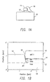
- FIG. 1A illustrates a tantalum nitride (TaN)/silicon nitride (SiN) resistor stack of the related art.
- Substrate 10 is shown having a layer 12 attached to substrate 10.
- Layer 12 is typically SiN.
- layer 14 is coupled.
- Layer 14 is typically TaN.
- metallization layer 16 is used to couple layer 14 to substrate 10.
- metallization layer 16 Since layer 12 is undercut with respect to layer 14 by the RIE etching process, metallization layer 16 must bridge the gap between layers 12 and 14. This gap does not provide proper support for metallization layer 16, and, as such, provides a stress point for metallization layer 16. Further, the height that metallization layer must span from the top of substrate 10 to the top of layer 14 is great (the "height" of the step is large), since layer 12 is sandwiched inbetween layer 14 and substrate 10. These factors lower the yield of devices and provide failure points for devices that survive initial fabrication and burn-in. Further, step coverage for metallization layer 16 is typically poor for devices using a structure as shown in FIG. 1A.
- FIG. 1B illustrates a calibrated simulation of the device described in FIG. 1A.
- the stress point 18 for metallization layer 16 shows a discontinuous metallization layer 16. This occurs because of the void 20 created by the undercutting of layer 12 during the etching process.
- thin films such as TaN
- metal evaporation is a line of sight technique, and liftoff is essentially based on shadowing of the evaporated metal by a retrograde photoresist profile and the breakage of the metal at the edge of the photoresist.
- the present invention discloses a thin film device and a method for fabricating film devices that can be used with HBT and HEMT technologies.
- the present invention is not limited to HBT and HEMT technologies, however, and, as such, provides a thin film device and a method for creating thin film devices in general.
- a method in accordance with the present invention comprises the steps of applying a first photoresist layer to a first surface, and patterning the first photoresist layer to have at least a first opening that exposes the first surface.
- a film is deposited onto the first photoresist layer, wherein a portion of the deposited film is deposited onto the exposed first surface.
- a second photoresist layer is applied onto the deposited layer, wherein the second photoresist layer is applied to the portion of the deposited film within the first opening and covers a second portion of the deposited layer.
- the deposited layer, first photoresist layer, and second photoresist layer are selectively removed, therein exposing the first surface and the second portion of the deposited layer.
- a device in accordance with the present invention comprises a device formed within a semiconductor structure and a deposited film, coupled to the device
- the deposited film is directly coupled to a first surface of a semiconductor wafer, wherein the semiconductor wafer contains the semiconductor structure, and the deposited film is defined by a first photoresist layer and a second photoresist layer.
- the first photoresist layer limits the coupling of the deposited film to the first surface, and the second photoresist layer defines a pattern of the deposited film.
- Thin film devices in accordance with the present invention and thin film devices fabricated in accordance with the present invention, are compatible with HBT and HEMT devices. Such devices and methods for making these devices provide devices that do not degrade the HBT and HEMT devices.
- the present invention incorporates thin film technology with integrated circuit device fabrication, including HEMT and HBT devices.
- the techniques of the present invention are also useful for other integrated circuits, such as bipolar junction transistors (BJTs), field effect transistors (FETs), junction FETs (JFETs), pseudomorphic HEMTs (PHEMTs), and metal-semiconductor FETs (MESFETs).
- BJTs bipolar junction transistors
- FETs field effect transistors
- JFETs junction FETs
- PHEMTs pseudomorphic HEMTs
- MESFETs metal-semiconductor FETs
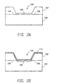
- FIGS. 2A-2E illustrate a device fabricated using the steps of the present invention.
- FIG. 2A illustrates first layer 100 of a semiconductor device.
- first layer 100 is shown as a wafer, first layer 100 can be a substrate, a dopant well within a substrate, an isolated structure on top of a layer, a layer or other structure, and is not limited to the single layer structure illustrated in FIG. 2A.
- Photoresist layer 102 is applied to first layer 100, and is photolithographically processed to produce an opening 104.
- the photolithographic process patterns the photoresist layer 102 by using masks and selective exposure to light, and the photoresist is selectively removed and hardened through a rinse and bake process.
- Opening 104 can appear in one or many places within photoresist layer 102, and a single opening 104 is shown for case of illustration. The present invention is not limited to a single opening 104 as shown in FIG. 2A.
- the covered areas 106 of first layer 100 can contain devices, such as HEMT and HBT devices, that will be protected by photoresist layer 102.
- the opening 104 size is not critical, so long as the opening 104 is large enough to accommodate whatever finished device is to be placed within opening 104 on the portion 108 of first layer 100.
- FIG. 2B illustrates a layer 110 deposited on photoresist layer 102 and within opening 104.
- Layer 110 is typically a thin film layer of tantalum nitride (TaN), but can also be a thin or thick film of other materials such as aluminum, silicon dioxide, nickel chromium, tungsten silicide, tungsten, silicon nitride, other metallizations, or other materials.
- Layer 110 is deposited using sputtering or other deposition techniques, such as evaporation for metals, plasma-enhanced chemical vapor deposition (PECVD), chemical vapor deposition (CVD), metal organic chemical vapor deposition (MOCVD), or other techniques.
- PECVD plasma-enhanced chemical vapor deposition
- CVD chemical vapor deposition
- MOCVD metal organic chemical vapor deposition
- FIG. 2C illustrates a second photoresist layer 112 that has been processed lithographically; Second photoresist layer 112 is used as a pattern defining layer for layer 110. Second photoresist layer 112 is processed as photoresist layer 102 was, using a different mask to produce a different pattern for second photoresist layer 112. Alternatively, the pattern for the second photoresist layer 112 can also be produced by image-reversing and properly shrinking the dimensions of the first mask photolithographically. The mesa structure shown in second photoresist layer 112 defines the pattern for layer 110 by protecting layer 110 during the etching process.
- FIG. 2D illustrates etching process 114 that removes the unprotected areas of layer 110.
- the etching process is typically a Reactive Ion Etch (RIE) process, but can be other processes such as wet etching, photoelectrochemical (PEC) etching, or other removal processes.
- RIE Reactive Ion Etch
- PEC photoelectrochemical
- Etching process 114 removes the layer 110, but not where second photoresist layer 112 protects layer 110. There may be some small undercutting of the second photoresist layer 112 during the etch process 114.
- first layer 100 that are exposed to the etch process 114 directly are the portions 109 that are not protected by second photoresist layer 112. As such, devices that are resident in areas 106 are protected from damage by photoresist layer 102.
- FIG. 2E illustrates a deposited thin film device 116 produced by the present invention.
- Photoresist layer 102 and second photoresist layer 112 are removed from first layer 100 by an acetone wash, or other wet or dry removal processes. These photoresist removal processes are not harmful to any devices that may be resident in areas 106 on the first layer 100, and, as such, leave device 116 intact in those areas 106. Further, photoresist removal processes do not harm layer 110, and leave layer 110 that was protected by second photoresist layer 112 attached to first layer 100.
- FIGS. 2A-2E allow for creation of thin film devices, such as resistors, to be fabricated without an underlying layer of SiN under layer 110.
- the underlying layer of SiN would be undercut by etch process 114, and, as such, make metallization contact to layer 110 difficult.
- the present invention provides a much lower step height 118, as well as a step height 118 that is not undercut, which provides better metallization contact with layer 110.
- the present invention refines the related process described in "Thin-film tantalum-nitride resistor technology for phosphide-based optoelectronics," M.L. Lovejoy, et al., Thin Solid Films 290-291 (1996), pages 513-517, because the present invention uses both photoresist layer 102 and second photoresist layer 112 to aid in defining the thin film pattern, unlike Lovejoy which uses the first photoresist layer to merely cover up devices already made on the wafer. As such, etching process times are reduced, and more precise thin film patterns arc possible
- the present invention does not require highly advanced photolithography techniques, nor does the present invention require a large number of processing steps to produce thin film devices on sensitive devices such as HEMTs and HBTs. As such, the present invention allows for a higher yield of thin film devices because of the increased reliability of the metallization step coverage and because of the relatively low number of processing steps required.
- the present invention also allows for the layer 110 to be up to seventy percent thinner than in the related art, i.e., step height 118 can be smaller, because the device that deposited layer 116 comprises is only one material, e.g., TaN, not TaN and SiN.
- the present invention is applicable to all semiconductor devices, because the photoresist described in photoresist layers 102 and 112 is used with other types of devices. Further, although discussed primarily with respect to thin film resistors, layer 110 can also produce other thin film devices or layers, The method of the present invention can also be applied several times in a serial fashion to produce a stack of deposited films, by repeating the photoresist protection of multiple layers 110.
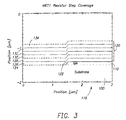
- FIG. 3 illustrates a simulated cross-section of the interconnect and thin film edge of the present invention.
- the device 116 with first layer 100 and layer 110, is shown in cross-section with a metallization layer 120.
- the simulation of the interface 122 is performed using a software tool called "Technology Computer Aided Design," written at the University of California, Berkeley, and is calibrated by the actual cross section of a SiN/TaN thin film device as described with respect to FIG. 1B.
- Examples of software design tools that arc commercially available include ATHENA, available from SILVACO, DIOS, available from ISE Corp., and TSUPREM-4 available from AVANT! Corp.
- Iso-contours 124-134 of 900 Angstrom thickness within metallization layer 120 show that there are no voids within metallization layer 120 at interface 122, which shows that the present invention provides good step coverage between the layer 110 and the metallization layer 120.
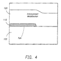
- the simulation shown in FIG. 3 correlates closely with actual devices manufactured using the present invention as illustrated in FIG. 4.
- FIG. 4 is an illustration of a scanning electron micrograph (SEM) of a cross-section of a resistor edge and metal interconnect prepared using the present invention.
- the contour of layer 110 and the contour of metallization layer 120 shown in FIG. 4 illustrate that a device made in accordance with the present invention shows no undercutting of layer 110, and, as such, no stress points on metallization layer 120 which can produce breakage.
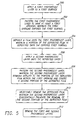
- FIG. 5 is a flow chart showing the operations used to practice one embodiment of the present invention.
- Block 200 represents performing the step of applying a first photoresist layer to a first surface.
- Block 202 represents performing the step of patterning the first photoresist layer to have at least a first opening in the first photoresist layer, wherein the first opening exposes the first surface.
- Block 204 represents performing the step of depositing a film onto the first photoresist layer, wherein a portion of the deposited film is deposited onto the exposed first surface.
- Block 206 represents performing the step of applying a second photoresist layer onto the deposited layer.
- Block 208 represents performing the step of patterning the second photoresist layer, wherein the second photoresist layer remains applied to the portion of the deposited film within the first opening and covers a second portion of the deposited layer.
- Block 210 represents performing the step of selectively removing the deposited layer, wherein the second photoresist layer substantially prevents the removal of the second portion of the deposited layer, wherein the first photoresist layer and the second photoresist layer assist in the defining of the deposited layer.
- Block 212 represents performing the step of removing the first photoresist layer and the second photoresist layer, therein exposing the first surface and the second portion of the deposited layer, wherein the first photoresist layer and the second photoresist layer assist in the defining of the deposited layer.
- a device in accordance with the present invention uses both photoresist layers to define the pattern of the deposited film.
- the Lovejoy reference uses the first photoresist layer merely to protect any underlying device.
- By using the two photoresist layers to define the deposited film more accurate contours of the film can be produced, as well as providing smaller undercutting of the thin film by reducing the areas of the film exposed to the etchant. Further, etching times are reduced, which reduces the risk of damage to other devices that are resident on the same substrate as the thin film device.
- a device made in accordance with the present invention will have better performance characteristics and more predictable operational response, than devices in the related art.
- the device of the present invention can also have multiple thin film layers by using two photoresist layers to define the pattern of each thin film layer of the final device.
- the layers can be patterned such that the thin film deposited first is patterned first, or patterned later than, subsequently deposited thin film layers.
- the present invention describes a device and a method for making a thin film device.
- a method in accordance with the present invention comprises the steps of applying a first photoresist layer to a first surface, and patterning the first photoresist layer to have at least a first opening that exposes the first surface.
- a film is deposited onto the first photoresist layer, wherein a portion of the deposited film is deposited onto the exposed first surface.
- a second photoresist layer is applied onto the deposited layer, wherein the second photoresist layer is applied to the portion of the deposited film within the first opening and covers a second portion of the deposited layer,
- the deposited layer, first photoresist layer, and second photoresist layer are selectively removed, therein exposing the first surface and the second portion of the deposited layer.
- a device in accordance with the present invention comprises a device formed within a semiconductor structure and a deposited film, coupled to the device,
- the deposited film is directly coupled to a first surface of a semiconductor wafer, wherein the semiconductor wafer contains the semiconductor structure, and the deposited film is defined by a first photoresist layer and a second photoresist layer.
- the first photoresist layer limits the coupling of the deposited film to the first surface, and the second photoresist layer defines a pattern of the deposited film.
Landscapes
- Junction Field-Effect Transistors (AREA)
- Bipolar Transistors (AREA)
- Drying Of Semiconductors (AREA)
- Semiconductor Integrated Circuits (AREA)
Abstract
Description
Claims (10)
- A method for fabricating integrated circuit thin films, characterized by the steps of:applying (200) a first photoresist layer (102) to a first surface (106, 108);patterning (202) the first photoresist layer (102) to have at least a first opening (104) in the first photoresist layer (102), wherein the first opening (104) exposes the first surface (106, 108);depositing (204) a film (110) onto the first photoresist layer (102), wherein a portion of the deposited film (110) is deposited onto the exposed first surface (108);applying (206) a second photoresist layer (112) onto the deposited layer (110);patterning (208) the second photoresist layer (112), wherein the second photoresist layer (112) remains applied to the portion of the deposited film (110) within the first opening (104) and covers a second portion of the deposited film (110);selectively removing (210) the deposited film (110), wherein the second photoresist layer (112) substantially prevents the removal of the second portion of the deposited film (110), wherein the first photoresist layer (102) and the second photoresist layer (112) assist in the defining of the deposited film (110); andremoving (212) the first photoresist layer (102) and the second photoresist layer (112), therein exposing the first surface (106, 108) and the second portion of the deposited film (110).
- The method of claim 1, characterized in that the deposited film (110) comprises a thin film resistor.
- The method of claim 1 or 2, characterized in that the deposited film (110) is comprised of a material selected from a group comprising tantalum nitride, aluminum, silicon dioxide, nickel chromium, tungsten silicide, tungsten, and silicon nitride.
- The method of any of claims 1 - 3, characterized in that the first photoresist layer (102) protects a device on the first surface (106).
- The method of claim 4, characterized in that the first surface (106) comprises at least a portion of a high electron mobility device.
- The method of claim 4, characterized in that the first surface comprises at least a portion of a heterojunction bipolar transistor.
- The method of any of claims 1 - 6, wherein the step (202) of patterning the first photoresist layer (102) and the step (208) of patterning the second photoresist layer (104) are performed using a single mask.
- A semiconductor device (116), characterized by:a device, formed within a semiconductor structure; anda deposited film (110), coupled to the device, wherein the deposited film (110) is directly coupled to a first surface (106, 108) of a semiconductor wafer (100), wherein the semiconductor wafer (100) contains the semiconductor structure, the deposited film (110) being defined by a first photoresist layer (102) and a second photoresist layer (112), the first photoresist layer (102) limiting the coupling of the deposited film (110) to the first surface, and the second photoresist layer (112) defining a pattern of the deposited film (110).
- The semiconductor device of claim 8, characterized in that the device is a high electron mobility transistor.
- The semiconductor device of claim 8, wherein the device is a heterojunction bipolar transistor.
Applications Claiming Priority (2)
| Application Number | Priority Date | Filing Date | Title |
|---|---|---|---|
| US436662 | 1989-11-15 | ||
| US43666299A | 1999-11-10 | 1999-11-10 |
Publications (3)
| Publication Number | Publication Date |
|---|---|
| EP1100120A2 true EP1100120A2 (en) | 2001-05-16 |
| EP1100120A3 EP1100120A3 (en) | 2004-02-04 |
| EP1100120B1 EP1100120B1 (en) | 2009-01-07 |
Family
ID=23733321
Family Applications (1)
| Application Number | Title | Priority Date | Filing Date |
|---|---|---|---|
| EP00124504A Expired - Lifetime EP1100120B1 (en) | 1999-11-10 | 2000-11-09 | Method for fabricating thin film devices |
Country Status (4)
| Country | Link |
|---|---|
| US (1) | US6916720B2 (en) |
| EP (1) | EP1100120B1 (en) |
| JP (1) | JP3413171B2 (en) |
| DE (1) | DE60041314D1 (en) |
Cited By (1)
| Publication number | Priority date | Publication date | Assignee | Title |
|---|---|---|---|---|
| WO2008059440A3 (en) * | 2006-11-14 | 2008-08-21 | Nxp Bv | Double patterning for lithography to increase feature spatial density |
Families Citing this family (2)
| Publication number | Priority date | Publication date | Assignee | Title |
|---|---|---|---|---|
| KR101066303B1 (en) * | 2004-09-09 | 2011-09-20 | 엘지디스플레이 주식회사 | Thin film transistor array substrate and manufacturing method thereof |
| JP7019922B2 (en) | 2018-06-07 | 2022-02-16 | 住友電工デバイス・イノベーション株式会社 | Manufacturing method of semiconductor device |
Family Cites Families (21)
| Publication number | Priority date | Publication date | Assignee | Title |
|---|---|---|---|---|
| JPS588579B2 (en) * | 1975-08-20 | 1983-02-16 | 松下電器産業株式会社 | hand tai souchi no seizou houhou |
| US4560435A (en) * | 1984-10-01 | 1985-12-24 | International Business Machines Corporation | Composite back-etch/lift-off stencil for proximity effect minimization |
| JPH0387026A (en) | 1988-12-13 | 1991-04-11 | Fujitsu Ltd | Manufacture of semiconductor device |
| EP0374036B1 (en) | 1988-12-13 | 1994-10-12 | Fujitsu Limited | Method of fabricating a semiconductor device using U.V. assisted selective multilayer etching |
| JPH03280552A (en) | 1990-03-29 | 1991-12-11 | Sanyo Electric Co Ltd | Manufacture of field effect transistor |
| EP0453785A1 (en) * | 1990-04-24 | 1991-10-30 | Oerlikon Contraves AG | Method of making multilayer thin film circuit comprising integrated thin film resistors |
| JPH0521467A (en) | 1991-07-09 | 1993-01-29 | Hitachi Ltd | Method for manufacturing field effect transistor |
| US5422307A (en) * | 1992-03-03 | 1995-06-06 | Sumitomo Electric Industries, Ltd. | Method of making an ohmic electrode using a TiW layer and an Au layer |
| US5525831A (en) | 1993-04-05 | 1996-06-11 | Nippondenso Co., Ltd. | Semiconductor device with thin film resistor having reduced film thickness sensitivity during trimming process |
| US5625218A (en) | 1994-06-17 | 1997-04-29 | Nippondenso Co., Ltd. | Semiconductor device equipped with a heat-fusible thin film resistor and production method thereof |
| US5554865A (en) | 1995-06-07 | 1996-09-10 | Hughes Aircraft Company | Integrated transmit/receive switch/low noise amplifier with dissimilar semiconductor devices |
| JP2825074B2 (en) | 1995-10-25 | 1998-11-18 | 日本電気株式会社 | Method for manufacturing semiconductor device |
| KR100206597B1 (en) * | 1995-12-29 | 1999-07-01 | 김영환 | Manufacturing method of fine pattern of semiconductor device |
| US5684308A (en) | 1996-02-15 | 1997-11-04 | Sandia Corporation | CMOS-compatible InP/InGaAs digital photoreceiver |
| JP3578547B2 (en) | 1996-04-18 | 2004-10-20 | 大阪瓦斯株式会社 | Combustion equipment |
| US5976944A (en) * | 1997-02-12 | 1999-11-02 | Harris Corporation | Integrated circuit with thin film resistors and a method for co-patterning thin film resistors with different compositions |
| US6096591A (en) * | 1997-06-30 | 2000-08-01 | Advanced Micro Devices, Inc. | Method of making an IGFET and a protected resistor with reduced processing steps |
| US6034411A (en) | 1997-10-29 | 2000-03-07 | Intersil Corporation | Inverted thin film resistor |
| US6015505A (en) * | 1997-10-30 | 2000-01-18 | International Business Machines Corporation | Process improvements for titanium-tungsten etching in the presence of electroplated C4's |
| JP4240424B2 (en) * | 1998-10-23 | 2009-03-18 | エルジー ディスプレイ カンパニー リミテッド | Etching agent and method for manufacturing substrate for electronic device using the same |
| US6081014A (en) | 1998-11-06 | 2000-06-27 | National Semiconductor Corporation | Silicon carbide chrome thin-film resistor |
-
2000
- 2000-11-09 DE DE60041314T patent/DE60041314D1/en not_active Expired - Lifetime
- 2000-11-09 EP EP00124504A patent/EP1100120B1/en not_active Expired - Lifetime
- 2000-11-10 JP JP2000343982A patent/JP3413171B2/en not_active Expired - Lifetime
-
2002
- 2002-07-05 US US10/190,223 patent/US6916720B2/en not_active Expired - Lifetime
Cited By (2)
| Publication number | Priority date | Publication date | Assignee | Title |
|---|---|---|---|---|
| WO2008059440A3 (en) * | 2006-11-14 | 2008-08-21 | Nxp Bv | Double patterning for lithography to increase feature spatial density |
| US8148052B2 (en) | 2006-11-14 | 2012-04-03 | Nxp B.V. | Double patterning for lithography to increase feature spatial density |
Also Published As
| Publication number | Publication date |
|---|---|
| US20020182818A1 (en) | 2002-12-05 |
| EP1100120B1 (en) | 2009-01-07 |
| JP3413171B2 (en) | 2003-06-03 |
| EP1100120A3 (en) | 2004-02-04 |
| JP2001196362A (en) | 2001-07-19 |
| US6916720B2 (en) | 2005-07-12 |
| DE60041314D1 (en) | 2009-02-26 |
Similar Documents
| Publication | Publication Date | Title |
|---|---|---|
| US6884704B2 (en) | Ohmic metal contact and channel protection in GaN devices using an encapsulation layer | |
| KR20200053465A (en) | Electrode structures for field effect transistors | |
| US9721793B2 (en) | Method of patterning without dummy gates | |
| JP3600544B2 (en) | Method for manufacturing semiconductor device | |
| US10181401B1 (en) | Method for manufacturing a semiconductor device | |
| JP2905500B2 (en) | Method for manufacturing semiconductor device | |
| US5338702A (en) | Method for fabricating tungsten local interconnections in high density CMOS | |
| US6916720B2 (en) | Thin film devices and method for fabricating thin film devices | |
| CN110581064A (en) | Manufacturing method of semiconductor device | |
| US5389564A (en) | Method of forming a GaAs FET having etched ohmic contacts | |
| CN114334642B (en) | Film patterning method and preparation method of semiconductor device | |
| JP2922066B2 (en) | Method for manufacturing semiconductor device | |
| JP2663902B2 (en) | Method for filling fine trench, method for manufacturing fine electrode, method for filling fine hole, and method for manufacturing fine metal wiring | |
| US5882992A (en) | Method for fabricating Tungsten local interconnections in high density CMOS circuits | |
| JPH03142970A (en) | Manufacture of semiconductor ic including both or either of bipolar heterojunction transistor and buried resistor | |
| CN1213162A (en) | Soft Passivation Layers in Semiconductor Manufacturing Technology | |
| JPH06283545A (en) | Method for contacting small features on an integrated circuit and heterojunction bipolar transistor according to the method | |
| US5136361A (en) | Stratified interconnect structure for integrated circuits | |
| EP0120918A1 (en) | ALUMINUM-METAL-SILICIDE CONNECTING STRUCTURE FOR INTEGRATED CIRCUITS AND THEIR PRODUCTION METHOD. | |
| JP2712340B2 (en) | Method for manufacturing semiconductor device | |
| JPH03205846A (en) | Manufacturing method of semiconductor device | |
| JP2002050757A (en) | Method for manufacturing semiconductor device | |
| JPS6020517A (en) | Manufacture of semiconductor device | |
| JPH0653249A (en) | Method for manufacturing semiconductor device | |
| JPH0462925A (en) | Semiconductor device |
Legal Events
| Date | Code | Title | Description |
|---|---|---|---|
| PUAI | Public reference made under article 153(3) epc to a published international application that has entered the european phase |
Free format text: ORIGINAL CODE: 0009012 |
|
| AK | Designated contracting states |
Kind code of ref document: A2 Designated state(s): AT BE CH CY DE DK ES FI FR GB GR IE IT LI LU MC NL PT SE TR |
|
| AX | Request for extension of the european patent |
Free format text: AL;LT;LV;MK;RO;SI |
|
| RAP1 | Party data changed (applicant data changed or rights of an application transferred) |
Owner name: THE BOEING COMPANY |
|
| PUAL | Search report despatched |
Free format text: ORIGINAL CODE: 0009013 |
|
| AK | Designated contracting states |
Kind code of ref document: A3 Designated state(s): AT BE CH CY DE DK ES FI FR GB GR IE IT LI LU MC NL PT SE TR |
|
| AX | Request for extension of the european patent |
Extension state: AL LT LV MK RO SI |
|
| RIC1 | Information provided on ipc code assigned before grant |
Ipc: 7H 01L 21/02 A Ipc: 7H 01L 21/8252 B |
|
| 17P | Request for examination filed |
Effective date: 20040727 |
|
| AKX | Designation fees paid |
Designated state(s): DE FR GB IT |
|
| 17Q | First examination report despatched |
Effective date: 20040927 |
|
| RIN1 | Information on inventor provided before grant (corrected) |
Inventor name: FIELDS, CHARLES H. Inventor name: KIZILOGLU, KURSAD Inventor name: SCHMITZ, ADELE E. |
|
| GRAP | Despatch of communication of intention to grant a patent |
Free format text: ORIGINAL CODE: EPIDOSNIGR1 |
|
| RIC1 | Information provided on ipc code assigned before grant |
Ipc: H01L 21/335 20060101ALI20080624BHEP Ipc: H01L 21/331 20060101ALI20080624BHEP Ipc: H01L 21/02 20060101AFI20080624BHEP |
|
| RTI1 | Title (correction) |
Free format text: METHOD FOR FABRICATING THIN FILM DEVICES |
|
| GRAS | Grant fee paid |
Free format text: ORIGINAL CODE: EPIDOSNIGR3 |
|
| GRAA | (expected) grant |
Free format text: ORIGINAL CODE: 0009210 |
|
| AK | Designated contracting states |
Kind code of ref document: B1 Designated state(s): DE FR GB IT |
|
| REG | Reference to a national code |
Ref country code: GB Ref legal event code: FG4D |
|
| REF | Corresponds to: |
Ref document number: 60041314 Country of ref document: DE Date of ref document: 20090226 Kind code of ref document: P |
|
| PLBE | No opposition filed within time limit |
Free format text: ORIGINAL CODE: 0009261 |
|
| STAA | Information on the status of an ep patent application or granted ep patent |
Free format text: STATUS: NO OPPOSITION FILED WITHIN TIME LIMIT |
|
| 26N | No opposition filed |
Effective date: 20091008 |
|
| REG | Reference to a national code |
Ref country code: FR Ref legal event code: PLFP Year of fee payment: 16 |
|
| REG | Reference to a national code |
Ref country code: FR Ref legal event code: PLFP Year of fee payment: 17 |
|
| REG | Reference to a national code |
Ref country code: FR Ref legal event code: PLFP Year of fee payment: 18 |
|
| PGFP | Annual fee paid to national office [announced via postgrant information from national office to epo] |
Ref country code: DE Payment date: 20191127 Year of fee payment: 20 |
|
| PGFP | Annual fee paid to national office [announced via postgrant information from national office to epo] |
Ref country code: IT Payment date: 20191125 Year of fee payment: 20 Ref country code: FR Payment date: 20191125 Year of fee payment: 20 |
|
| PGFP | Annual fee paid to national office [announced via postgrant information from national office to epo] |
Ref country code: GB Payment date: 20191127 Year of fee payment: 20 |
|
| REG | Reference to a national code |
Ref country code: DE Ref legal event code: R071 Ref document number: 60041314 Country of ref document: DE |
|
| REG | Reference to a national code |
Ref country code: GB Ref legal event code: PE20 Expiry date: 20201108 |
|
| PG25 | Lapsed in a contracting state [announced via postgrant information from national office to epo] |
Ref country code: GB Free format text: LAPSE BECAUSE OF EXPIRATION OF PROTECTION Effective date: 20201108 |