EP1100033A2 - Method and system for determining operator staffing - Google Patents
Method and system for determining operator staffing Download PDFInfo
- Publication number
- EP1100033A2 EP1100033A2 EP00309576A EP00309576A EP1100033A2 EP 1100033 A2 EP1100033 A2 EP 1100033A2 EP 00309576 A EP00309576 A EP 00309576A EP 00309576 A EP00309576 A EP 00309576A EP 1100033 A2 EP1100033 A2 EP 1100033A2
- Authority
- EP
- European Patent Office
- Prior art keywords
- operators
- work center
- operator
- determining
- needed
- Prior art date
- Legal status (The legal status is an assumption and is not a legal conclusion. Google has not performed a legal analysis and makes no representation as to the accuracy of the status listed.)
- Withdrawn
Links
Images


Classifications
-
- G—PHYSICS
- G06—COMPUTING OR CALCULATING; COUNTING
- G06Q—INFORMATION AND COMMUNICATION TECHNOLOGY [ICT] SPECIALLY ADAPTED FOR ADMINISTRATIVE, COMMERCIAL, FINANCIAL, MANAGERIAL OR SUPERVISORY PURPOSES; SYSTEMS OR METHODS SPECIALLY ADAPTED FOR ADMINISTRATIVE, COMMERCIAL, FINANCIAL, MANAGERIAL OR SUPERVISORY PURPOSES, NOT OTHERWISE PROVIDED FOR
- G06Q10/00—Administration; Management
- G06Q10/06—Resources, workflows, human or project management; Enterprise or organisation planning; Enterprise or organisation modelling
-
- G—PHYSICS
- G05—CONTROLLING; REGULATING
- G05B—CONTROL OR REGULATING SYSTEMS IN GENERAL; FUNCTIONAL ELEMENTS OF SUCH SYSTEMS; MONITORING OR TESTING ARRANGEMENTS FOR SUCH SYSTEMS OR ELEMENTS
- G05B19/00—Program-control systems
- G05B19/02—Program-control systems electric
- G05B19/418—Total factory control, i.e. centrally controlling a plurality of machines, e.g. direct or distributed numerical control [DNC], flexible manufacturing systems [FMS], integrated manufacturing systems [IMS] or computer integrated manufacturing [CIM]
- G05B19/41865—Total factory control, i.e. centrally controlling a plurality of machines, e.g. direct or distributed numerical control [DNC], flexible manufacturing systems [FMS], integrated manufacturing systems [IMS] or computer integrated manufacturing [CIM] characterised by job scheduling, process planning, material flow
-
- G—PHYSICS
- G05—CONTROLLING; REGULATING
- G05B—CONTROL OR REGULATING SYSTEMS IN GENERAL; FUNCTIONAL ELEMENTS OF SUCH SYSTEMS; MONITORING OR TESTING ARRANGEMENTS FOR SUCH SYSTEMS OR ELEMENTS
- G05B2219/00—Program-control systems
- G05B2219/30—Nc systems
- G05B2219/31—From computer integrated manufacturing till monitoring
- G05B2219/31425—Plan availability of operator for cell as function of time and operation calendar
-
- G—PHYSICS
- G05—CONTROLLING; REGULATING
- G05B—CONTROL OR REGULATING SYSTEMS IN GENERAL; FUNCTIONAL ELEMENTS OF SUCH SYSTEMS; MONITORING OR TESTING ARRANGEMENTS FOR SUCH SYSTEMS OR ELEMENTS
- G05B2219/00—Program-control systems
- G05B2219/30—Nc systems
- G05B2219/32—Operator till task planning
- G05B2219/32262—Work manhours, number of operators and work place
-
- G—PHYSICS
- G05—CONTROLLING; REGULATING
- G05B—CONTROL OR REGULATING SYSTEMS IN GENERAL; FUNCTIONAL ELEMENTS OF SUCH SYSTEMS; MONITORING OR TESTING ARRANGEMENTS FOR SUCH SYSTEMS OR ELEMENTS
- G05B2219/00—Program-control systems
- G05B2219/30—Nc systems
- G05B2219/45—Nc applications
- G05B2219/45031—Manufacturing semiconductor wafers
-
- Y—GENERAL TAGGING OF NEW TECHNOLOGICAL DEVELOPMENTS; GENERAL TAGGING OF CROSS-SECTIONAL TECHNOLOGIES SPANNING OVER SEVERAL SECTIONS OF THE IPC; TECHNICAL SUBJECTS COVERED BY FORMER USPC CROSS-REFERENCE ART COLLECTIONS [XRACs] AND DIGESTS
- Y02—TECHNOLOGIES OR APPLICATIONS FOR MITIGATION OR ADAPTATION AGAINST CLIMATE CHANGE
- Y02P—CLIMATE CHANGE MITIGATION TECHNOLOGIES IN THE PRODUCTION OR PROCESSING OF GOODS
- Y02P90/00—Enabling technologies with a potential contribution to greenhouse gas [GHG] emissions mitigation
- Y02P90/02—Total factory control, e.g. smart factories, flexible manufacturing systems [FMS] or integrated manufacturing systems [IMS]
Definitions
- the present invention relates to the field of product manufacturing, and, more particularly, to manufacturing of semiconductor wafers.
- Manufacturing Information Systems are systems that contain data and data processing methods that aid manufacturing managers in production planning and execution.
- an MIS typically contains demand data, supply data, cost data, and bill-of-material data.
- Manufacturing Resource Planning (MRP), Capacity Requirements Planning (CRP) and Enterprise Resource Planning (ERP) are types of MISs.
- An MIS is primarily a data management system. Most important manufacturing decisions are still ultimately made by humans; however, software that processes all the relevant data and uses mathematical techniques to determine optimal, feasible production plans can save millions of dollars for manufacturers.
- ERPs may track and manage a multi-profile workforce, process attendance parameters, allocate actual cost records, optimize resource utilization and measure labor productivity throughout the enterprise. Furthermore, workplace logistics, production planning, material management, sales, project accounting, human resources and payroll may also be managed with such systems.
- Semiconductor devices also called integrated circuits, are manufactured and mass produced by fabricating identical circuit patterns on a single semiconductor wafer. During the process, the wafer is cut into identical dies or chips. Although commonly referred to as semiconductor devices, the devices are fabricated from various materials, including conductors (e.g. copper, aluminum and tungsten), non-conductors (e.g. silicon dioxide) and semiconductors (e.g. silicon). Within an integrated circuit, thousands of devices (e.g., transistors, diodes) are formed.
- conductors e.g. copper, aluminum and tungsten
- non-conductors e.g. silicon dioxide
- semiconductors e.g. silicon
- the integrated circuit devices with their various conductive layers, semiconductive layers, insulating layers, contacts and interconnects are formed by fabrication processes, including doping processes, deposition processes, photolithographic processes, etching processes and other processes.
- fabrication processes including doping processes, deposition processes, photolithographic processes, etching processes and other processes.
- Many operators are needed at various process stations (e.g. a group of machines) in the fab to sustain a given production volume.
- U.S. Patent No. 5,140,537 to Tullis and entitled "Modeling a Factory with Human Operators and Validating the Model” is directed to a computer simulation of a semiconductor factory.
- the simulation includes comparatively evaluating individual lots as they move through process sequences over time.
- Historical records of staffing are used to determine staff levels to include in the model.
- a typical semiconductor fab includes a lot tracking system.
- a lot is a group of wafers which are typically processed together.
- Computer software running on a local area network is used to collect data regarding product flow in order to keep track of individual and groups of lots as they move through the processing stations in a work center.
- AccuFACTS 9000 from Santa Barbara Analysis, Inc., of Valencia, California is a shop floor lot tracking software product which collects real time data regarding works in progress, lot locations and processing station inventory, for example.
- time studies are based on the detailed observation of all the operators activities, the classification of the activities, and the measurement or estimation of the time needed to perform all of them. These studies are very slow and expensive, and they are discontinuous and thus do not provide frequent or accurate tracking of manpower.
- the work center includes a wafer lot tracking system and a plurality of processing stations for processing a plurality of lots of semiconductor wafers to be manufactured.
- the method includes the steps of setting the wafer manufacturing goal, determining a highest operator throughput as a maximum rate of wafers that can be processed per operator based on data from the lot tracking system, and determining a minimum number of operators that are needed to process wafers in the work center to achieve the manufacturing goal based on the wafer manufacturing goal and the highest operator throughput.
- the method further includes the determination of a number of working operators needed to process wafers in the semiconductor wafer work center to achieve the wafer manufacturing goal by increasing the minimum number of operators based on characteristics of the processing stations. An operator availability based on an average number of working operators and a number of all operators at the work center is also determined. The total number of operators needed at the semiconductor wafer work center to achieve the wafer manufacturing goal is then determined based on the operator availability and the number of working operators.
- the step of determining the total number of operators needed at the semiconductor wafer work center to achieve the wafer manufacturing goal may also be based on a work center operating time and a working time per operator. Also, the step of determining the total number of operators needed at the semiconductor wafer work center to achieve the wafer manufacturing goal may comprise multiplying the quotient of the number of working operators needed divided by the operator availability, by the quotient of the work center operating time divided by the working time per operator.
- the step of setting the wafer manufacturing goal may be based on a rate of wafers that can be started in a product flow and a number of process steps in the product flow.
- the step of determining the number of working operators may comprise dividing the minimum number of operators by an operator cushion.
- the operator cushion is preferably between 0 and 1 and may be a historical factor.
- the step of determining the minimum number of operators may comprise dividing the wafer manufacturing goal by the highest operator throughput.
- the step of determining the operator availability may comprise dividing the average number of working operators by the number of all operators at the work center.
- the work center includes a wafer lot tracking system and a plurality of processing stations for processing a plurality of lots of semiconductor wafers to be manufactured.
- the system includes means for determining a highest operator throughput as a maximum rate of wafers that can be processed per operator based on data from the lot tracking system, and means for determining a minimum number of operators that are needed to process wafers in the work center to achieve the manufacturing goal based on the wafer manufacturing goal and the highest operator throughput.
- the system also includes means for determining a number of working operators that are needed to process wafers in the work center to achieve the wafer manufacturing goal by increasing the minimum number of operators based on characteristics of the processing stations, and means for determining an operator availability based on an average number of working operators and a number of all operators at the work center. Furthermore, the system includes means for determining the total number of operators needed at the semiconductor wafer work center to achieve the wafer manufacturing goal based on the operator availability and the number of working operators.
- the means for determining the total number of operators needed at the semiconductor work center to achieve the wafer manufacturing goal may also be based on a work center operating time and a working time per operator.
- the means for determining the total number of operators needed at the semiconductor work center to achieve the wafer manufacturing goal may be for multiplying the quotient of the number of working operators needed divided by the operator availability, by the quotient of the work center operating time divided by the working time per operator.
- the wafer manufacturing goal may be based on a rate of wafers that can be started in a product flow and a number of process steps in the product flow.
- the means for determining the number of working operators may be for dividing the minimum number of operators by an operator cushion.
- the operator cushion is preferably between 0 and 1 and may be a historical factor.
- the means for determining the minimum number of operators may be for dividing the wafer manufacturing goal by the highest operator throughput, and the means for determining the operator availability may be for dividing the average number of working operators by the number of all operators at the work center.
- FIG. 1 is a bar graph illustrating an example of the staffing variability for a work center.
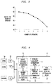
- FIG. 2 is a graph illustrating an example of throughput variation with respect to staffing variation for a work center.
- FIG. 3 is a graph illustrating an example of throughput per operator for a work center.
- FIG. 4 is a block diagram illustrating a system for determining a total number of operators needed at the work center to achieve a manufacturing goal in accordance with the present invention.
- FIG. 5 is a flowchart illustrating the preferred steps for determining the total number of operators needed at the work center to achieve the manufacturing goal in accordance with the present invention.
- the work center includes a wafer lot tracking system 22 and a plurality of processing stations 24 operated by the a team of operators for processing a plurality of lots of semiconductor wafers to be manufactured as would be appreciated by those skilled in the art.
- processing stations 24 include, for example, doping process stations, deposition process stations, photolithographic process stations, etching process stations and other process stations as are conventionally known.
- the method and system 10 automatically provide for the quantification of the total number of operators needed without direct observation. This reduces costs, decreases the time needed, and allows for a continuous tracking of manpower.
- the method and system 10 use data from the computerized lot tracking system 22 in the work center, as discussed above. Data, from the lot tracking system 22 and corresponding to the variability of manpower in the work center, is used for certain measurements. For example, the number of different operators performing processes every hour and their distribution can be measured as represented by the graph of FIG. 1. An average number of working operators can be determined from the measurement and this graph.
- Such data can also be obtained from the lot tracking system 22 , as would readily be appreciated by those skilled in the art, and an example is represented in FIG. 2.
- staffing variability has a significant impact in work center throughput. For example, with two operators, about 20 units may be processed, while about 100 units may be processed with seven or eight operators. From this data, the number of wafers processed by each operator per hour at each staffing level can be obtained, for example, as shown in the graph of FIG. 3.
- a higher operator throughput i.e. throughput per operator
- the method begins at Block 30 and a manufacturing goal is set at Block 32 .
- the manufacturing goal may be expressed, for example, in terms of wafers per hour (WPH) in a semiconductor fab.
- WPH wafers per hour
- WPH may be expressed as the summation of S r times V r , for r from 1 to n; where S r is the number of wafers to be started per hour in the product flow r, and V r is the number of steps in the product flow r in a work center.
- the system 10 includes a highest-operator-throughput determination means 12 which determines the highest operator throughput (HOT) in Block 34 of the method.
- HOT may be defined as the maximum rate of wafers (e.g. wafers per hour) that can be processed per operator based on data from the lot tracking system, as can be seen in FIG. 3, for example.
- the system 10 also includes a minimum-number-of-operators determination means 14 for determining a minimum number of operators (MOR) that are needed (Block 36 ) to process wafers in the work center to achieve the manufacturing goal based on the manufacturing goal and the highest operator throughput (HOT).
- MOR WPH/HOT.
- MOR is may be defined as the minimum number of operators simultaneously processing wafers in the work center that are needed to achieve the manufacturing goal.
- An operator availability (OA) based on an average number of working operators (M) and a number of all operators (P) at the work center is then determined (Block 40 ) by an operator-availability-determination-means 16 .
- the total number of operators (S) needed at the semiconductor wafer work center to achieve the wafer manufacturing goal is then determined (Block 42 ) by the total-number-of-operators determination means 20 based on the operator availability (OA) and the number of working operators (OR) before ending the method at Block 44 .
- the step (Block 42 ) of determining the total number of operators needed (S) may also be based on a work center operating time (OH) and a working time per operator (WH).
- the step (Block 42 ) of determining the total number of operators needed (S) at the semiconductor wafer work center to achieve the wafer manufacturing goal may comprise multiplying the quotient of the number of working operators needed divided by the operator availability (OR/OA), by the quotient of the work center operating time divided by the working time per operator (OH/WH).
- S (OR/OA) x (OH/OA).
- the above described system 10 including the various means 12 , 14 , 16 , 18 , 20 is preferably implemented as computer software as would be understood by the skilled artisan. It may be a module of a computerized lot tracking system or Enterprise Resource Planning system. Additionally, the various means 12 , 14 , 16 , 18 , 20 may be embodied as a discrete logic circuit as also would be appreciated by those skilled in the art. Many modifications and other embodiments of the invention will come to the mind of one skilled in the art having the benefit of the teachings presented in the foregoing descriptions and the associated drawings. Therefore, it is understood that the invention is not to be limited to the specific embodiments disclosed, and that modifications and embodiments are intended to be included within the scope of the appended claims.
Landscapes
- Engineering & Computer Science (AREA)
- Business, Economics & Management (AREA)
- Economics (AREA)
- Strategic Management (AREA)
- Human Resources & Organizations (AREA)
- Quality & Reliability (AREA)
- Physics & Mathematics (AREA)
- General Physics & Mathematics (AREA)
- Entrepreneurship & Innovation (AREA)
- Educational Administration (AREA)
- Operations Research (AREA)
- Automation & Control Theory (AREA)
- Game Theory and Decision Science (AREA)
- Manufacturing & Machinery (AREA)
- General Engineering & Computer Science (AREA)
- Marketing (AREA)
- Development Economics (AREA)
- Tourism & Hospitality (AREA)
- General Business, Economics & Management (AREA)
- Theoretical Computer Science (AREA)
- General Factory Administration (AREA)
- Management, Administration, Business Operations System, And Electronic Commerce (AREA)
- Container, Conveyance, Adherence, Positioning, Of Wafer (AREA)
Abstract
Description
- The present invention relates to the field of product manufacturing, and, more particularly, to manufacturing of semiconductor wafers.
- Manufacturing Information Systems (MISs) are systems that contain data and data processing methods that aid manufacturing managers in production planning and execution. For example, an MIS typically contains demand data, supply data, cost data, and bill-of-material data. Manufacturing Resource Planning (MRP), Capacity Requirements Planning (CRP) and Enterprise Resource Planning (ERP) are types of MISs. An MIS is primarily a data management system. Most important manufacturing decisions are still ultimately made by humans; however, software that processes all the relevant data and uses mathematical techniques to determine optimal, feasible production plans can save millions of dollars for manufacturers.
- ERPs may track and manage a multi-profile workforce, process attendance parameters, allocate actual cost records, optimize resource utilization and measure labor productivity throughout the enterprise. Furthermore, workplace logistics,
production planning, material management, sales, project accounting, human resources and payroll may also be managed with such systems. - Semiconductor devices, also called integrated circuits, are manufactured and mass produced by fabricating identical circuit patterns on a single semiconductor wafer. During the process, the wafer is cut into identical dies or chips. Although commonly referred to as semiconductor devices, the devices are fabricated from various materials, including conductors (e.g. copper, aluminum and tungsten), non-conductors (e.g. silicon dioxide) and semiconductors (e.g. silicon). Within an integrated circuit, thousands of devices (e.g., transistors, diodes) are formed.
- In a semiconductor fabrication plant (fab), the integrated circuit devices with their various conductive layers, semiconductive layers, insulating layers, contacts and interconnects are formed by fabrication processes, including doping processes, deposition processes, photolithographic processes, etching processes and other processes. Many operators are needed at various process stations (e.g. a group of machines) in the fab to sustain a given production volume.
- For example, U.S. Patent No. 5,140,537 to Tullis and entitled "Modeling a Factory with Human Operators and Validating the Model" is directed to a computer simulation of a semiconductor factory. The simulation includes comparatively evaluating individual lots as they move through process sequences over time. Historical records of staffing are used to determine staff levels to include in the model.
- Additionally, a typical semiconductor fab includes a lot tracking system. A lot is a group of wafers which are typically processed together. Computer software running on a local area network is used to collect data regarding product flow in order to keep track of individual and groups of lots as they move through the processing stations in a work center. For example, AccuFACTS 9000 from Santa Barbara Analysis, Inc., of Valencia, California is a shop floor lot tracking software product which collects real time data regarding works in progress, lot locations and processing station inventory, for example.
- Typically, in the semiconductor manufacturing industry, the number of operators needed is calculated through the use of time studies. Such time studies are based on the detailed observation of all the operators activities, the classification of the activities, and the measurement or estimation of the time needed to perform all of them. These studies are very slow and expensive, and they are discontinuous and thus do not provide frequent or accurate tracking of manpower.
- In view of the foregoing background, it is therefore an object of the invention to provide a method and system for quickly and continuously determining a total number of operators needed at a work center to achieve a manufacturing goal.
- This and other objects, features and advantages in accordance with the present invention are provided by a method of determining a total number of operators needed at a semiconductor wafer work center to achieve a wafer manufacturing goal. The work center includes a wafer lot tracking system and a plurality of processing stations for processing a plurality of lots of semiconductor wafers to be manufactured. The method includes the steps of setting the wafer manufacturing goal, determining a highest operator throughput as a maximum rate of wafers that can be processed per operator based on data from the lot tracking system, and determining a minimum number of operators that are needed to process wafers in the work center to achieve the manufacturing goal based on the wafer manufacturing goal and the highest operator throughput.
- The method further includes the determination of a number of working operators needed to process wafers in the semiconductor wafer work center to achieve the wafer manufacturing goal by increasing the minimum number of operators based on characteristics of the processing stations. An operator availability based on an average number of working operators and a number of all operators at the work center is also determined. The total number of operators needed at the semiconductor wafer work center to achieve the wafer manufacturing goal is then determined based on the operator availability and the number of working operators.
- The step of determining the total number of operators needed at the semiconductor wafer work center to achieve the wafer manufacturing goal may also be based on a work center operating time and a working time per operator. Also, the step of determining the total number of operators needed at the semiconductor wafer work center to achieve the wafer manufacturing goal may comprise multiplying the quotient of the number of working operators needed divided by the operator availability, by the quotient of the work center operating time divided by the working time per operator. The step of setting the wafer manufacturing goal may be based on a rate of wafers that can be started in a product flow and a number of process steps in the product flow.
- Additionally, the step of determining the number of working operators may comprise dividing the minimum number of operators by an operator cushion. The operator cushion is preferably between 0 and 1 and may be a historical factor. The step of determining the minimum number of operators may comprise dividing the wafer manufacturing goal by the highest operator throughput. Also, the step of determining the operator availability may comprise dividing the average number of working operators by the number of all operators at the work center.
- The objects, features and advantages in accordance with the present invention are also provided by a system for determining a total number of operators needed at a semiconductor wafer work center to achieve a wafer manufacturing goal. Again, the work center includes a wafer lot tracking system and a plurality of processing stations for processing a plurality of lots of semiconductor wafers to be manufactured. The system includes means for determining a highest operator throughput as a maximum rate of wafers that can be processed per operator based on data from the lot tracking system, and means for determining a minimum number of operators that are needed to process wafers in the work center to achieve the manufacturing goal based on the wafer manufacturing goal and the highest operator throughput.
- The system also includes means for determining a number of working operators that are needed to process wafers in the work center to achieve the wafer manufacturing goal by increasing the minimum number of operators based on characteristics of the processing stations, and means for determining an operator availability based on an average number of working operators and a number of all operators at the work center. Furthermore, the system includes means for determining the total number of operators needed at the semiconductor wafer work center to achieve the wafer manufacturing goal based on the operator availability and the number of working operators.
- The means for determining the total number of operators needed at the semiconductor work center to achieve the wafer manufacturing goal may also be based on a work center operating time and a working time per operator. The means for determining the total number of operators needed at the semiconductor work center to achieve the wafer manufacturing goal may be for multiplying the quotient of the number of working operators needed divided by the operator availability, by the quotient of the work center operating time divided by the working time per operator. Again, the wafer manufacturing goal may be based on a rate of wafers that can be started in a product flow and a number of process steps in the product flow.
- The means for determining the number of working operators may be for dividing the minimum number of operators by an operator cushion. Again, the operator cushion is preferably between 0 and 1 and may be a historical factor. Also, the means for determining the minimum number of operators may be for dividing the wafer manufacturing goal by the highest operator throughput, and the means for determining the operator availability may be for dividing the average number of working operators by the number of all operators at the work center.
- FIG. 1 is a bar graph illustrating an example of the staffing variability for a work center.
- FIG. 2 is a graph illustrating an example of throughput variation with respect to staffing variation for a work center.
- FIG. 3 is a graph illustrating an example of throughput per operator for a work center.
- FIG. 4 is a block diagram illustrating a system for determining a total number of operators needed at the work center to achieve a manufacturing goal in accordance with the present invention.
- FIG. 5 is a flowchart illustrating the preferred steps for determining the total number of operators needed at the work center to achieve the manufacturing goal in accordance with the present invention.
- The present invention will now be described more fully hereinafter with reference to the accompanying drawings, in which preferred embodiments of the invention are shown. This invention may, however, be embodied in many different forms and should not be construed as limited to the embodiments set forth herein. Rather, these embodiments are provided so that this disclosure will be thorough and complete, and will fully convey the scope of the invention to those skilled in the art. Like numbers refer to like elements throughout.
- Referring to FIGS. 1-5, the method and
system 10 for determining a total number of operators needed at a semiconductor wafer work center to achieve a wafer manufacturing goal, will be described. The work center includes a waferlot tracking system 22 and a plurality ofprocessing stations 24 operated by the a team of operators for processing a plurality of lots of semiconductor wafers to be manufactured as would be appreciated by those skilled in the art.Such processing stations 24 include, for example, doping process stations, deposition process stations, photolithographic process stations, etching process stations and other process stations as are conventionally known. - The method and
system 10 automatically provide for the quantification of the total number of operators needed without direct observation. This reduces costs, decreases the time needed, and allows for a continuous tracking of manpower. The method andsystem 10 use data from the computerizedlot tracking system 22 in the work center, as discussed above. Data, from thelot tracking system 22 and corresponding to the variability of manpower in the work center, is used for certain measurements. For example, the number of different operators performing processes every hour and their distribution can be measured as represented by the graph of FIG. 1. An average number of working operators can be determined from the measurement and this graph. - The average work center throughput changes for different staffing levels. Such data can also be obtained from the
lot tracking system 22, as would readily be appreciated by those skilled in the art, and an example is represented in FIG. 2. As shown in the graph of FIG. 2, staffing variability has a significant impact in work center throughput. For example, with two operators, about 20 units may be processed, while about 100 units may be processed with seven or eight operators. From this data, the number of wafers processed by each operator per hour at each staffing level can be obtained, for example, as shown in the graph of FIG. 3. As shown, a higher operator throughput (i.e. throughput per operator) can be achieved with the minimum number of operators in the work center because each operator will likely always have an available processing station and the materials needed for the particular process. - With specific reference to FIGS. 4 and 5, the basic steps of the method, and the parts of the
system 10 of the invention will now be described. The method begins atBlock 30 and a manufacturing goal is set atBlock 32. The manufacturing goal may be expressed, for example, in terms of wafers per hour (WPH) in a semiconductor fab. For example, WPH may be expressed as the summation of Sr times Vr, for r from 1 to n; where Sr is the number of wafers to be started per hour in the product flow r, and Vr is the number of steps in the product flow r in a work center. Thesystem 10 includes a highest-operator-throughput determination means 12 which determines the highest operator throughput (HOT) inBlock 34 of the method. HOT may be defined as the maximum rate of wafers (e.g. wafers per hour) that can be processed per operator based on data from the lot tracking system, as can be seen in FIG. 3, for example. - The
system 10 also includes a minimum-number-of-operators determination means 14 for determining a minimum number of operators (MOR) that are needed (Block 36) to process wafers in the work center to achieve the manufacturing goal based on the manufacturing goal and the highest operator throughput (HOT). In other words: MOR = WPH/HOT. MOR is may be defined as the minimum number of operators simultaneously processing wafers in the work center that are needed to achieve the manufacturing goal. - However, in a typical work center, processing stations may experience a certain amount of idle time due to the probability that they will wait to be loaded or unloaded while operators perform other tasks. Thus the
system 10 includes a number-of-working-operators determination means 18 for determining a number of working operators needed (OR) to process wafers (Block 38) in the semiconductor wafer work center to achieve the wafer manufacturing goal by increasing the minimum number of operators (MOR) based on characteristics of the processing stations. These characteristics include process time, bottlenecks, etc. as would be appreciated by the skilled artisan. For example: OR = MOR/C; where C is a an operator cushion based on experience (i.e. a historical factor). Typically, C would be between 0 and 1. - An operator availability (OA) based on an average number of working operators (M) and a number of all operators (P) at the work center is then determined (Block 40) by an operator-availability-determination-
means 16. M is, for example, determined from the data represented in FIG. 1. Due to training, meetings, lunches, breaks etc., not all the operators at the fab are processing wafers. Thus, preferably: OA = M/P. - The total number of operators (S) needed at the semiconductor wafer work center to achieve the wafer manufacturing goal is then determined (Block 42) by the total-number-of-operators determination means 20 based on the operator availability (OA) and the number of working operators (OR) before ending the method at
Block 44. The step (Block 42) of determining the total number of operators needed (S) may also be based on a work center operating time (OH) and a working time per operator (WH). For example, the step (Block 42) of determining the total number of operators needed (S) at the semiconductor wafer work center to achieve the wafer manufacturing goal may comprise multiplying the quotient of the number of working operators needed divided by the operator availability (OR/OA), by the quotient of the work center operating time divided by the working time per operator (OH/WH). In other words: S = (OR/OA) x (OH/OA). - The above described
system 10 including the various means 12, 14, 16, 18, 20 is preferably implemented as computer software as would be understood by the skilled artisan. It may be a module of a computerized lot tracking system or Enterprise Resource Planning system. Additionally, the various means 12, 14, 16, 18, 20 may be embodied as a discrete logic circuit as also would be appreciated by those skilled in the art. Many modifications and other embodiments of the invention will come to the mind of one skilled in the art having the benefit of the teachings presented in the foregoing descriptions and the associated drawings. Therefore, it is understood that the invention is not to be limited to the specific embodiments disclosed, and that modifications and embodiments are intended to be included within the scope of the appended claims.
Claims (12)
- A method of determining a total number of operators needed at a work center to achieve a manufacturing goal, the work center including a product tracking system and a plurality of processing stations for processing products to be manufactured, the method comprising the steps of:setting the manufacturing goal;determining a highest operator throughput as a maximum rate of products that can be processed per operator based on data from the product tracking system;determining a minimum number of operators that are needed to process products in the work center to achieve the manufacturing goal based on the manufacturing goal and the highest operator throughput;determining a number of working operators that are needed to process products in the work center to achieve the manufacturing goal by increasing the minimum number of operators based on characteristics of the processing stations;determining an operator availability based on an average number of working operators processing products and a number of all operators at the work center; anddetermining the total number of operators needed at the work center to achieve the manufacturing goal based on the operator availability and the number of working operators.
- A method according to Claim 1, wherein the step of determining the total number of operators needed at the work center to achieve the manufacturing goal is also based on a work center operating time and a working time per operator.
- A method according to Claim 2, wherein the step of determining the total number of operators needed at the work center to achieve the manufacturing goal comprises multiplying the quotient of the number of working operators needed divided by the operator availability, by the quotient of the work center operating time divided by the working time per operator.
- A method as claimed in any of the preceding claims including the step of setting the manufacturing goal.
- A method according to Claim 4, wherein the step of setting the manufacturing goal is based on a rate of products that can be started in a product flow and a number of process steps in the product flow.
- A method according to any of the preceding claims, wherein the step of determining the number of working operators comprises dividing the minimum number of operators by an operator cushion.
- A method according to Claim 6, wherein the operator cushion is between 0 and 1.
- A method according to Claim 6, wherein the operator cushion is a historical factor.
- A method according to any of the preceding claims, wherein the step of determining the minimum number of operators comprises dividing the manufacturing goal by the highest operator throughput.
- A method according to any of the preceding claims, wherein the step of determining the operator availability comprises dividing the average number of working operators by the number of all operators at the work center.
- A method as claimed in any of the preceding claims wherein the work centre is a semiconductor wafer work center, the products are wafers and the tracking system is a wafer lot tracking system.
- A system for determining a total number of operators needed at a work center to achieve a manufacturing goal, the work center including a product tracking system and a plurality of processing stations for processing products to be manufactured, the system comprising means for carrying out the steps of a method as claimed in any of the preceding claims.
Applications Claiming Priority (2)
| Application Number | Priority Date | Filing Date | Title |
|---|---|---|---|
| US439048 | 1999-11-12 | ||
| US09/439,048 US6459946B1 (en) | 1999-11-12 | 1999-11-12 | Method and system for determining operator staffing |
Publications (2)
| Publication Number | Publication Date |
|---|---|
| EP1100033A2 true EP1100033A2 (en) | 2001-05-16 |
| EP1100033A3 EP1100033A3 (en) | 2003-04-02 |
Family
ID=23743070
Family Applications (1)
| Application Number | Title | Priority Date | Filing Date |
|---|---|---|---|
| EP00309576A Withdrawn EP1100033A3 (en) | 1999-11-12 | 2000-10-30 | Method and system for determining operator staffing |
Country Status (2)
| Country | Link |
|---|---|
| US (1) | US6459946B1 (en) |
| EP (1) | EP1100033A3 (en) |
Families Citing this family (16)
| Publication number | Priority date | Publication date | Assignee | Title |
|---|---|---|---|---|
| US20020059089A1 (en) * | 2000-08-31 | 2002-05-16 | Toyota Jidosha Kabushiki Kaisha | Supply plan drafting device, method of drafting supply plan, program for drafting supply plan, and method of drafting production plan |
| AU2002248486A1 (en) * | 2001-02-20 | 2002-09-04 | Ronald Jon Lander | Time studies chronometer with generic activity descriptions |
| US8015042B2 (en) * | 2001-04-02 | 2011-09-06 | Verint Americas Inc. | Methods for long-range contact center staff planning utilizing discrete event simulation |
| US20030055706A1 (en) * | 2001-08-15 | 2003-03-20 | Beth Statfeld | System and method for determining staffing needs for functions in an office |
| US7343353B1 (en) * | 2002-08-02 | 2008-03-11 | Taiwan Semiconductor Manufacturing Company, Ltd. | Method to turn off machines during-turn down period while achieving minimum cost and required cycle time |
| US20040107133A1 (en) * | 2002-12-02 | 2004-06-03 | Pershing Investments, Llc. | Capacity planning method and system |
| US20050021384A1 (en) * | 2002-12-02 | 2005-01-27 | Pershing Investments, Llc | Capacity planning method and system with approved accuracy and confidence indication |
| US20040138940A1 (en) * | 2003-01-10 | 2004-07-15 | Aybar Manuel A. | Labor model for a production line |
| US6772030B1 (en) * | 2003-05-05 | 2004-08-03 | Taiwan Semiconductor Mfg. Co., Ltd. | Method of considering equipment constraints in a manufacturing planning system |
| US7245978B2 (en) * | 2003-07-18 | 2007-07-17 | Fuji Machine Mfg. Co., Ltd. | Managing apparatus for managing assisting work to assist substrate-related-work performing system, and managing program for managing assisting work to assist substrate-related-work performing system |
| US7175777B1 (en) * | 2003-12-02 | 2007-02-13 | National Semiconductor Corporation | Method of forming a sub-micron tip feature |
| CN1716263B (en) * | 2004-06-30 | 2013-02-06 | 通用电气公司 | System and method for auxiliary dispatch of computer using coordinating surrogate |
| JP2008112209A (en) * | 2006-10-27 | 2008-05-15 | Omron Corp | Operating state monitoring device, operating state monitoring method, and program |
| US9354630B2 (en) * | 2011-05-19 | 2016-05-31 | Universal Laser Systems, Inc. | Flexible laser manufacturing systems and associated methods of use and manufacture |
| JP5960644B2 (en) * | 2013-05-27 | 2016-08-02 | Ckd株式会社 | Monitoring system |
| US11415970B2 (en) * | 2018-03-09 | 2022-08-16 | Nec Corporation | Control planning device, control planning system, control planning method, and recording medium |
Family Cites Families (14)
| Publication number | Priority date | Publication date | Assignee | Title |
|---|---|---|---|---|
| US5212635A (en) * | 1989-10-23 | 1993-05-18 | International Business Machines Corporation | Method and apparatus for measurement of manufacturing technician efficiency |
| US5140537A (en) | 1990-05-21 | 1992-08-18 | Hewlett-Packard Company | Modeling a factory with human operators and validating the model |
| US5442561A (en) | 1992-05-12 | 1995-08-15 | Nippon Telegraph And Telephone Corporation | Production management system and its application method |
| US5615138A (en) | 1993-04-08 | 1997-03-25 | Honda Giken Kogyo Kabushiki Kaisha | Method for establishing the working mantime in the production line |
| US5444632A (en) | 1994-04-28 | 1995-08-22 | Texas Instruments Incorporated | Apparatus and method for controlling and scheduling processing machines |
| US5787000A (en) * | 1994-05-27 | 1998-07-28 | Lilly Software Associates, Inc. | Method and apparatus for scheduling work orders in a manufacturing process |
| US5617342A (en) | 1994-11-14 | 1997-04-01 | Elazouni; Ashraf M. | Discrete-event simulation-based method for staffing highway maintenance crews |
| JP3315844B2 (en) * | 1994-12-09 | 2002-08-19 | 株式会社東芝 | Scheduling device and scheduling method |
| JPH10207939A (en) * | 1997-01-17 | 1998-08-07 | Nec Corp | Workflow system |
| JPH10261122A (en) * | 1997-03-18 | 1998-09-29 | Sumitomo Wiring Syst Ltd | Work distribution optimization method |
| US5971585A (en) * | 1997-09-09 | 1999-10-26 | International Business Machines Corporation | Best can do matching of assets with demand in microelectronics manufacturing |
| US6049742A (en) * | 1997-09-26 | 2000-04-11 | International Business Machines Corporation | Projected supply planning matching assets with demand in microelectronics manufacturing |
| US6041267A (en) * | 1997-09-26 | 2000-03-21 | International Business Machines Corporation | Method to provide common support for multiple types of solvers for matching assets with demand in microelectronics manufacturing |
| US6259959B1 (en) * | 1998-09-04 | 2001-07-10 | International Business Machines Corporation | Method for determining the performance components of a manufacturing line |
-
1999
- 1999-11-12 US US09/439,048 patent/US6459946B1/en not_active Expired - Lifetime
-
2000
- 2000-10-30 EP EP00309576A patent/EP1100033A3/en not_active Withdrawn
Non-Patent Citations (1)
| Title |
|---|
| No Search * |
Also Published As
| Publication number | Publication date |
|---|---|
| US6459946B1 (en) | 2002-10-01 |
| EP1100033A3 (en) | 2003-04-02 |
Similar Documents
| Publication | Publication Date | Title |
|---|---|---|
| US6459946B1 (en) | Method and system for determining operator staffing | |
| Jeong et al. | A real-time scheduling mechanism for a flexible manufacturing system: using simulation and dispatching rules | |
| Uzsoy et al. | A review of production planning and scheduling models in the semiconductor industry part II: Shop-floor control | |
| US6259959B1 (en) | Method for determining the performance components of a manufacturing line | |
| Hundal | Product costing: a comparison of conventional and activity-based costing methods | |
| Chou et al. | A methodology for product mix planning in semiconductor foundry manufacturing | |
| US20070117230A1 (en) | Computer readable storage medium for work-in-process schedules | |
| Dietrich | A taxonomy of discrete manufacturing systems | |
| US20220404817A1 (en) | Processes for controlling operation of machine tools | |
| Yadav et al. | Evaluation of batching and layout on the performance of flexible manufacturing system | |
| US6920366B1 (en) | Heuristics for efficient supply chain planning in a heterogeneous production line | |
| Hung et al. | Determining safety stocks for production planning in uncertain manufacturing | |
| Shahabudeen et al. | Design of a two-card dynamic kanban system using a simulated annealing algorithm | |
| Seidel et al. | Challenges associated with realization of lot level fab out forecast in a giga wafer fabrication plant | |
| Lee et al. | Manufacturing cycle time reduction using balance control in the semiconductor fabrication line | |
| Grewal et al. | Integrating targeted cycle-time reduction into the capital planning process | |
| Qi et al. | Impact of production control and system factors in semiconductor wafer fabrication | |
| Ehm et al. | The global supply chain is our new fab: Integration and automation challenges | |
| Meyersdorf et al. | Cycle time reduction for semiconductor wafer fabrication facilities | |
| Rulkens et al. | Batch size optimization of a furnace and pre-clean area by using dynamic simulations | |
| Shewchuk et al. | Flexibility and manufacturing system design: an experimental investigation | |
| US7257502B1 (en) | Determining metrology sampling decisions based on fabrication simulation | |
| Bahri et al. | Automated material handling system traffic control by means of node balancing | |
| US8126767B1 (en) | System and method for tuning a segmented model representating product flow through a supply chain or manufacturing process | |
| Lamghari-Idrissi et al. | Influence of spare parts service measures on the performance of front-end wafer production process |
Legal Events
| Date | Code | Title | Description |
|---|---|---|---|
| PUAI | Public reference made under article 153(3) epc to a published international application that has entered the european phase |
Free format text: ORIGINAL CODE: 0009012 |
|
| AK | Designated contracting states |
Kind code of ref document: A2 Designated state(s): AT BE CH CY DE DK ES FI FR GB GR IE IT LI LU MC NL PT SE |
|
| AX | Request for extension of the european patent |
Free format text: AL;LT;LV;MK;RO;SI |
|
| PUAL | Search report despatched |
Free format text: ORIGINAL CODE: 0009013 |
|
| AK | Designated contracting states |
Kind code of ref document: A3 Designated state(s): AT BE CH CY DE DK ES FI FR GB GR IE IT LI LU MC NL PT SE Designated state(s): AT BE CH CY DE DK ES FI FR GB GR IE IT LI LU MC NL PT SE |
|
| AX | Request for extension of the european patent |
Extension state: AL LT LV MK RO SI |
|
| STAA | Information on the status of an ep patent application or granted ep patent |
Free format text: STATUS: THE APPLICATION IS DEEMED TO BE WITHDRAWN |
|
| 18D | Application deemed to be withdrawn |
Effective date: 20030503 |