EP1099974A2 - Optical scanning apparatus and image-forming apparatus - Google Patents
Optical scanning apparatus and image-forming apparatus Download PDFInfo
- Publication number
- EP1099974A2 EP1099974A2 EP00124540A EP00124540A EP1099974A2 EP 1099974 A2 EP1099974 A2 EP 1099974A2 EP 00124540 A EP00124540 A EP 00124540A EP 00124540 A EP00124540 A EP 00124540A EP 1099974 A2 EP1099974 A2 EP 1099974A2
- Authority
- EP
- European Patent Office
- Prior art keywords
- lens
- image
- optical
- scanning
- mirror
- Prior art date
- Legal status (The legal status is an assumption and is not a legal conclusion. Google has not performed a legal analysis and makes no representation as to the accuracy of the status listed.)
- Granted
Links
Images





Classifications
-
- G—PHYSICS
- G02—OPTICS
- G02B—OPTICAL ELEMENTS, SYSTEMS OR APPARATUS
- G02B26/00—Optical devices or arrangements for the control of light using movable or deformable optical elements
- G02B26/08—Optical devices or arrangements for the control of light using movable or deformable optical elements for controlling the direction of light
- G02B26/10—Scanning systems
- G02B26/12—Scanning systems using multifaceted mirrors
- G02B26/125—Details of the optical system between the polygonal mirror and the image plane
Definitions
- the present invention relates to an optical scanning apparatus and, more particularly, to prevention of flare from a scanning mirror in the optical scanning apparatus used in printers in which an image is drawn with laser light.
- Fig. 8 is an optical path diagram of a conventional optical scanning apparatus.
- Reference numeral 91 designates a laser unit, 92 a cylindrical lens, 93 a scanning mirror, 94 a spherical lens, 95 a toric lens, and 96 a photosensitive drum.
- Parallel laser light emitted from the laser unit 91 is converged only in the sub-scanning direction by the cylindrical lens 92 to impinge on a surface of the scanning mirror 93.
- the scanning mirror 93 rotates at a constant speed and the light reflected by the scanning mirror 93 travels through the spherical lens 94 and the toric lens 95 to undergo correction for F ⁇ , whereby converging light scans the surface on the photosensitive drum 96.
- the photosensitive drum 96 rotates at a constant speed in synchronism with a driving signal of the semiconductor laser and the scanning light forms an electrostatic latent image on the photosensitive drum 96. An image is printed from this electrostatic latent image onto paper by the electrophotographic process.
- the scanning efficiency of the polygon mirror is increased by illuminating the polygon mirror with a beam greater than the main scanning width of the polygon mirror (an overfield optical system), for example, as disclosed in Japanese Patent Application Laid-Open No. 6-143677.
- the scanning efficiency of the polygon can be increased by this method, but there arises a problem that spot sizes are nonuniform depending upon image heights.
- An effective method for relaxing this nonuniformity is to make the beam incident to the polygon mirror from in a plane made by the rotation axis of the polygon and the optical axis of the f ⁇ lens. This can minimize the nonuniformity of the spot, as compared with that in the case of incidence from other positions, and the spot becomes symmetric with respect to the image heights.
- the width of the incident beam is made greater than the width of the reflective facets of the polygon, there will arise a problem that reflected light from an adjacent facet appears as flare at the image plane to deteriorate the image.
- An object of the present invention is, therefore, to maintain sufficient rays in the portion of the polygon mirror associated with the formation of image and efficiently intercept the reflected light from the surface not associated with the image.
- a distal end of a shield member is located within a predetermined range determined by a diameter ⁇ of an inscribed circle to the polygon and a focal length f of the f ⁇ lens or the like.
- An optical scanning apparatus is an optical scanning apparatus comprising a scanning mirror having a plurality of reflective facets for deflectively reflecting a first beam emitted from a laser light source and an f ⁇ lens for focusing a second beam deflectively reflected by a reflective facet of said scanning mirror, in a spot shape on an image plane, wherein a width in a main scanning direction of the first beam incident to said scanning mirror is wider than a width of the reflective facets of said scanning mirror in the main scanning direction, said optical scanning apparatus including a shield member for intercepting a third beam reflected by a reflective facet adjacent to the reflective facet deflectively reflecting the second beam.
- the first beam travels through said f ⁇ lens to be incident to said scanning mirror and the first beam incident to the scanning mirror is present within a plane made by a rotation axis of the scanning mirror and the optical axis of the f ⁇ lens.
- an x-coordinate axis is taken along the optical axis of the first beam of incident rays
- the positive direction of the x-coordinate axis is taken along a direction in which the second beam and third beam of reflected rays from the scanning mirror travel
- a distal end of said shield member is located in the range defined by the following equation between the reflective facet of the scanning mirror and a ray output surface of the f ⁇ lens: [Eq. 1] ⁇ x + ⁇ ⁇
- said shield member is means for positioning said f ⁇ lens.
- said shield member is a portion of a lens surface in a noneffective image portion of said f ⁇ lens, said portion being treated by a light-intercepting treatment.
- said shield member is formed so as to be integral with an optical box.
- an x-coordinate axis is taken along the optical axis of the first beam of incident rays, the positive direction of the x-coordinate axis along a direction in which the second beam and third beam of reflected rays from the scanning mirror travel, and a y-coordinate axis along the main scanning direction, a distal end of said shield member is located in the range defined by the following equation between the f ⁇ lens and said image plane: [Eq. 2] ⁇ x + ⁇ ⁇
- An image-forming apparatus is an image-forming apparatus comprising the optical scanning apparatus as set forth, a photosensitive body placed on a surface to be scanned, a developing unit for developing an electrostatic latent image formed on said photosensitive body with the beam under scanning by said optical scanning apparatus, into a toner image, a transfer unit for transferring said developed toner image onto a transfer medium, and a fixing unit for fixing the transferred toner image on the transfer medium.
- Another image-forming apparatus is an image-forming apparatus comprising the optical scanning apparatus as set forth, and a printer controller for converting code data supplied from an external device, into an image signal and supplying the image signal to said optical scanning apparatus.
- Fig. 1 is an optical path diagram in the main scanning direction of the optical scanning apparatus in the first embodiment.
- Fig. 2 is an optical path diagram in the sub-scanning direction of the optical scanning apparatus in the first embodiment.
- reference numeral 1 designates a laser light source, 2 a collimator lens, 3 a stop, 4 a cylindrical lens, 5 an f ⁇ lens, 6 a scanning mirror, 7 a cylindrical mirror, and 8 the image plane such as a photosensitive drum or the like.
- the laser light emitted from the laser light source 1 is converted into nearly parallel light by the collimator lens 2 and the beam is restricted by the stop 3.
- the beam is converged only in the sub-scanning direction by the cylindrical lens 4 and then travels through the f6 lens 5 to be converged on a line near a reflective facet of the scanning mirror.
- the scanning mirror 6 rotates at a constant speed to deflect the laser light.
- the laser light thus deflected is incident again to the f ⁇ lens 5 having the F ⁇ characteristic and the beam is converged thereby in the main scanning direction.
- the light emerging from the f ⁇ lens is converged in the sub-scanning direction by the cylindrical mirror 7 having a power in the sub-scanning direction to form a spot on the image plane 8.
- Fig. 3 is a development of rays in the main scanning direction in the optical scanning apparatus of the first embodiment.
- Numeral 21 denotes the laser light source, 22 the collimator lens, 23 the stop, 24 the cylindrical lens, 25 the f6 lens, 26 the reflective facet of the scanning mirror, 27 the cylindrical mirror, and 28 the image plane such as the photosensitive drum or the like.
- the laser light emitted from the light source 21 is converged into nearly parallel light by the collimator lens 22 and the beam is restricted by the stop 23 to travel through the cylindrical lens 24 having no power in the main scanning direction, into the f ⁇ lens 25.
- the f ⁇ lens 25 has the power in the main scanning direction to convert the light into a beam further closer to parallel light.
- the light emerging from the f ⁇ lens 25 is incident to the reflective facet 26 of the polygon mirror to be deflectively reflected in part.
- the light reflected by the polygon is incident again to the f ⁇ lens 25 to be converged in the main scanning direction.
- the f ⁇ lens 25 corrects the F ⁇ characteristic depending upon angles of deflection at the reflective facet of the polygon.
- the light emerging from the f ⁇ lens is reflected by the cylindrical mirror having no power in the main scanning direction to form a spot on the image plane 28. Since the polygon mirror 26 rotates in the direction of arrow R, the spot on the image plane 8 scans the surface in the direction of arrow S.
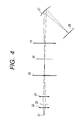
- Fig. 4 is a development of rays in the sub-scanning direction in the optical scanning apparatus of the first embodiment.
- the laser light emitted from the light source 21 is converged into nearly parallel light by the collimator lens 22 and the beam is restricted by the stop 23.
- the beam determined by the stop 23 is converged in the sub-scanning direction by the cylindrical lens 24 having the power in the sub-scanning direction, travels through the f ⁇ lens having little power in the sub-scanning direction, and thereafter is linearly focused as a linear image elongated in the main scanning direction on the reflective facet 26 of the polygon mirror.
- the light reflected by the reflective facet 26 of the polygon mirror is incident to the f ⁇ lens 25.
- the f ⁇ lens 25 has little power in the sub-scanning direction, and the light travels through the f ⁇ lens 25 and thereafter enters the cylindrical mirror 27 having the power in the sub-scanning direction.
- the light incident to the cylindrical mirror 27 is converged in the sub-scanning direction to form the spot on the image plane 28. Since the polygon mirror 26 and the image plane 28 are in optically conjugate relation herein, the optical system is a tilt correction system wherein there is no deviation of the image position in the sub-scanning direction against tilt of the polygon facet.
- Fig. 5 is an enlarged view in the main scanning direction of the vicinity of the scanning mirror in the optical scanning apparatus of the first embodiment.
- Numeral 31 represents a first beam incident to the polygon being the scanning mirror, 32 a reflective facet of the polygon, 33 the polygon, 34 a shield member for cutting flare (third beam), and 35 a beam reflected by the reflective facet 32 and then entering the f ⁇ lens.
- the second beam 35 indicated by hatching in the beam guided to the reflective facet 32 by the incidence optical system is incident to the f ⁇ lens and is reflected by the unrepresented cylindrical mirror to form the spot on the image plane. Since the beam incident to the polygon 33 is greater than the width of the polygon facets (overfield optical system), there exists the third beam 37 reflected by an adjacent facet 36. This beam 37 will adversely affect the image if it reaches the image plane.
- the shield member 34 surrounds the periphery of the polygon mirror 33 so as to cut the unwanted flare.
- n represents the number of polygon facets
- f the focal length of the f ⁇ lens
- y 0 the maximum image height in the main scanning direction (the outermost ray of the second beam)
- ⁇ the diameter of the inscribed circle to the polygon.
- Fig. 6 is a graph to show the range of location of the distal end of the shield member.
- f 318 mm
- 150 mm
- ⁇ 26 mm
- n 12.
- the flare which can negatively affect the image, can efficiently be cut by placing the distal end of the shield member anywhere in the hatched range of Fig. 6 so as to intercept the light apart from the optical axis.
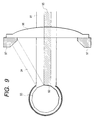
- Fig. 9 is an explanatory diagram to show another shield method of Embodiment 1.
- numeral 91 designates the first beam incident to the polygon mirror, 92 a reflective facet of the polygon mirror, 93 the polygon mirror, 94 the flare being the third beam reflected from a facet adjacent to the facet reflecting the rays associated with the formation of image, and 95 the reflected beam of the second beam, which is the beam reflected by the polygon mirror facet 92, traveling through the f ⁇ lens 96, and thereafter entering the photosensitive drum or the like to form an image thereon.
- Numeral 96 denotes the f ⁇ lens and 97 a positioning member (mount member) of the f ⁇ lens.
- the positioning member (mount member) 97 of the f ⁇ lens with the shield function is placed in the range satisfying above Eq. 3.
- the flare which is reflected from the adjacent facet to the reflective facet reflecting the beam 95 associated with the formation of image in the polygon 93, can perfectly be cut by constructing the opaque lens positioning member 97 in such a shape as to prevent the flare from reaching the drum surface and as not to intercept the light associated with the formation of image.
- the positioning member 97 is desirably one being opaque and preferably giving rise to no reflected light.
- the material is resin such as opaque polycarbonate or the like, or metal such as aluminum or the like, and in either case it is desirable to stick a flocked sheet thereonto or coat it with an antireflection film, in a sense of preventing the flare from entering the photosensitive drum because of multiple reflection.
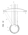
- Fig. 10 is an explanatory diagram to illustrate another shield method of Embodiment 1 of the present invention.
- numeral 11 designates the first beam incident to the polygon mirror, 12 a reflective facet of the polygon mirror, 13 the polygon mirror, 18 the flare being the third beam reflected from the adjacent facet to the facet reflecting the rays associated with the formation of image, and 15 the reflected beam of the second beam, which is the beam reflected by the polygon mirror facet 12, traveling through the f ⁇ lens 16, and thereafter entering the photosensitive drum or the like to form an image thereon.
- Numeral 17 denotes a shield film for cutting the unwanted flare without use of an additional member, which is made by forming a roughened surface for shielding in the surface of the lens or by applying an oily black paint for shielding onto the surface.
- the shield film 17 is placed in the noneffective image portion in the periphery of the f ⁇ lens 16 and within the range satisfying above Eq. 3.
- Fig. 10 shows the treatment for shielding on the entrance side of the lens, but the same effect can also be achieved by placing the shield film on the exit side of the lens. However, if the dimensional accuracy is severe in the optical-axis direction of the lens, the film is desirably placed on the side that is not associated with positioning.
- the shield member was placed adjacent to the lens in the present embodiment, but the like effect can also be attained by forming part of the optical box in the shape intercepting the light in the optical path of the flare or by processing a lid of the optical box in the shape intercepting the optical path of the flare.
- the shield member of the present invention may also be formed so as to be integral with the optical box.
- Fig. 7 is an optical path diagram in the main scanning direction for explaining the position of the shield member in the optical scanning apparatus of the second embodiment.
- Numeral 51 designates the first beam incident to the polygon mirror, 52 a reflective facet of the polygon mirror, 53 the polygon mirror, 54 the flare (third beam) reflected from a facet adjacent to the facet reflecting the rays associated with the formation of image, 55 the second beam of reflected light, which is the beam reflected by the polygon mirror facet 52, entering the f ⁇ lens, thereafter reflected by the cylinder mirror or the like, and then entering the photosensitive drum or the like to form an image, 56 the f ⁇ lens, and 57 the shield member for cutting the unwanted flare.
- the beam 55 indicated by hatching is incident to the f ⁇ lens and is reflected by the unrepresented cylindrical mirror to form a spot on the image plane, thereby scanning the image plane with rotation of the polygon mirror. Since the beam incident to the polygon mirror 53 is greater than the width of the polygon facets (overfield optical system), there exists a beam 54 reflected by the adjacent facet. This beam 54 will adversely affect the image if it reaches the image plane. Therefore, the unwanted flare is cut by placing the shield member 57 in a predetermined range between the f ⁇ lens and the photosensitive drum surface in order to intercept the unwanted, reflected light as illustrated in Fig. 7.
- n indicates the number of polygon facets, f the focal length of the f ⁇ lens, y 0 the maximum image height in the main scanning direction, ⁇ the diameter of the inscribed circle to the polygon, and x 1 the position of the rear principal plane of the f ⁇ lens.
- Fig. 11 is a graph to show the range in which the distal end of the shield member is to be located.
- f 318 mm
- y 150 mm
- ⁇ 26 mm
- n 12
- x 1 80 mm.
- the flare which can adversely affect the image, can efficiently be cut by intercepting the light apart from the optical axis by the tip of the shield member located anywhere in the hatched range of Fig. 11.
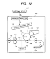
- Fig. 12 is a cross-sectional view of the principal part along the sub-scanning direction to show an embodiment of the image-forming apparatus of the present invention.
- numeral 104 designates the image-forming apparatus.
- This image-forming apparatus 104 accepts input of code data Dc from an external device 117 such as a personal computer or the like.
- This code data Dc is converted into image data (dot data) Di by a printer controller 111 in the apparatus.
- This image data Di is supplied to an optical scanning unit 100 having the structure as described in either of Embodiments 1 and 2.
- This optical scanning unit 100 outputs an optical beam 103 modulated according to the image data Di and this light beam 103 scans a photosensitive surface of photosensitive drum 101 in the main scanning direction.
- the photosensitive drum 101 as an electrostatic latent image carrier (photosensitive body) is rotated clockwise by a motor 115. With the rotation thereof, the photosensitive surface of the photosensitive drum 101 moves in the sub-scanning direction perpendicular to the main scanning direction, relative to the light beam 103.
- a charging roller 102 for uniformly charging the surface of the photosensitive drum 101 is disposed so as to contact the surface. Then the surface of the photosensitive drum 101 charged by the charging roller 102 is exposed to the light beam 103 under scanning by the optical scanning unit 100.
- the light beam 103 is modulated based on the image data Di and an electrostatic latent image is formed on the surface of the photosensitive drum 101 under irradiation with this light beam 103.
- This electrostatic latent image is developed into a toner image by a developing unit 107 disposed so as to contact the photosensitive drum 101 downstream in the rotating direction of the photosensitive drum 101 from the irradiation position of the light beam 103.
- the toner image developed by the developing unit 107 is transferred onto a sheet 112 being a transfer medium, by a transfer roller 108 opposed to the photosensitive drum 101 below the photosensitive drum 101.
- Sheets 112 are stored in a sheet cassette 109 in front of (i.e., on the right side in Fig. 12) of the photosensitive drum 101, but sheet feed can also be implemented by hand feeding.
- a sheet feed roller 110 is disposed at an end of the sheet cassette 109 and feeds each sheet 112 in the sheet cassette 109 into the conveyance path.
- the fixing unit is composed of a fixing roller 113 having a fixing heater (not illustrated) inside and a pressing roller 114 disposed in press contact with the fixing roller 113 and heats while pressing the sheet 112 thus conveyed from the transfer part, in the nip part between the fixing roller 113 and the pressing roller 114 to fix the unfixed toner image on the sheet 112.
- Sheet discharge rollers 116 are disposed further behind the fixing roller 113 to discharge the fixed sheet 112 to the outside of the image-forming apparatus.
- the print controller 111 also performs control of each section in the image-forming apparatus, including the motor 115, and control of the polygon motor etc. in the optical scanning unit described above, in addition to the conversion of data described above.
- the tip portion of the shield member is positioned in the certain range determined by the inside diameter of the polygon and the focal length of the f ⁇ lens, whereby the flare is cut efficiently. This permits a good image to be formed without flare.
Landscapes
- Physics & Mathematics (AREA)
- General Physics & Mathematics (AREA)
- Optics & Photonics (AREA)
- Mechanical Optical Scanning Systems (AREA)
- Facsimile Scanning Arrangements (AREA)
- Laser Beam Printer (AREA)
Abstract
Description
wherein a width in a main scanning direction of the first beam incident to said scanning mirror is wider than a width of the reflective facets of said scanning mirror in the main scanning direction,
said optical scanning apparatus including a shield member for intercepting a third beam reflected by a reflective facet adjacent to the reflective facet deflectively reflecting the second beam.
Claims (9)
- An optical scanning apparatus comprising a scanning mirror having a plurality of reflective facets for deflectively reflecting a first beam emitted from a laser light source and an f6 lens for focusing a second beam deflectively reflected by a reflective facet of said scanning mirror, in a spot shape on an image plane,
wherein a width in a main scanning direction of the first beam incident to said scanning mirror is wider than a width of the reflective facets of said scanning mirror in the main scanning direction,
said optical scanning apparatus including a shield member for intercepting a third beam reflected by a reflective facet adjacent to the reflective facet deflectively reflecting the second beam. - The optical scanning apparatus according to Claim 1, wherein the first beam travels through said f lens to be incident to said scanning mirror and the first beam incident to the scanning mirror is present within a plane made by a rotation axis of the scanning mirror and the optical axis of the f lens.
- The optical scanning apparatus according to Claim 2, wherein, where the origin is set at the center of the rotation axis of said scanning mirror, an x-coordinate axis is taken along the optical axis of the first beam of incident rays, the positive direction of the x-coordinate axis is taken along a direction in which the second beam and third beam of reflected rays from the scanning mirror travel, and a y-coordinate axis along the main scanning direction, a distal end of said shield member is located in the range defined by the following equation between the reflective facet of the scanning mirror and a ray output surface of the f lens:where n is the number of facets of a polygon being the scanning mirror, f a focal length of the f lens, y0 a maximum image height in the main scanning direction, and a diameter of an inscribed circle to the polygon.αx + β ≤ |y| ≤ α'x + β'α = tan20β = (sec20) × (acos0 - 2sin0)/2α' = tan21β' = (-sec21) × (acos1 + 2sin1)/20 = y0/2f1 = 2π/n - 0a = tan(π/n),
- The optical scanning apparatus according to Claim 3, wherein said shield member is means for positioning said f lens.
- The optical scanning apparatus according to Claim 3, wherein said shield member is a portion of a lens surface in a noneffective image portion of said f lens, said portion being treated by a light-intercepting treatment.
- The optical scanning apparatus according to Claim 3, wherein said shield member is formed so as to be integral with an optical box.
- The optical scanning apparatus according to Claim 2, wherein, where the origin is set at the center of the rotation axis of said scanning mirror, an x-coordinate axis is taken along the optical axis of the first beam of incident rays, the positive direction of the x-coordinate axis along a direction in which the second beam and third beam of reflected rays from the scanning mirror travel, and a y-coordinate axis along the main scanning direction, a distal end of said shield member is located in the range defined by the following equation between the f lens and said image plane:where n is the number of facets of a polygon being the scanning mirror, f a focal length of the f lens, y0 a maximum image height in the main scanning direction, a diameter of an inscribed circle to the polygon, and x1 a position of a rear principal plane of the f lens.αx + β ≤ |y| ≤ α'x + β'α = 2(2f0cos20 + sin0 - x1sin20)/(cos0 + 2fcos20)β = 2f0 - [2(f + x1)(2f0cos20 + sin0 - x1sin20)/(cos0 + 2fcos20)]α' = 2(2f1cos21 + sin1 - x1sin20)/(-cos1 + 2fcos21)β' = 2f1 + [2(f + x1)(2f1cos21 + sin1 - x1sin21)/(cos1 - 2fcos21)]0 = y0/2f1 = 2π/n - 0a = tan(π/n),
- An image-forming apparatus comprising the optical scanning apparatus as set forth in either one of Claims 1 to 7, a photosensitive body placed on a surface to be scanned, a developing unit for developing an electrostatic latent image formed on said photosensitive body with the beam under scanning by said optical scanning apparatus, into a toner image, a transfer unit for transferring said developed toner image onto a transfer medium, and a fixing unit for fixing the transferred toner image on the transfer medium.
- An image-forming apparatus comprising the optical scanning apparatus as set forth in either one of Claims 1 to 7, and a printer controller for converting code data supplied from an external device, into an image signal and supplying the image signal to said optical scanning apparatus.
Applications Claiming Priority (4)
| Application Number | Priority Date | Filing Date | Title |
|---|---|---|---|
| JP31860999 | 1999-11-09 | ||
| JP31860999 | 1999-11-09 | ||
| JP2000336236A JP3673709B2 (en) | 1999-11-09 | 2000-11-02 | Optical scanning apparatus and image forming apparatus |
| JP2000336236 | 2000-11-02 |
Publications (3)
| Publication Number | Publication Date |
|---|---|
| EP1099974A2 true EP1099974A2 (en) | 2001-05-16 |
| EP1099974A3 EP1099974A3 (en) | 2002-07-10 |
| EP1099974B1 EP1099974B1 (en) | 2005-02-16 |
Family
ID=26569429
Family Applications (1)
| Application Number | Title | Priority Date | Filing Date |
|---|---|---|---|
| EP00124540A Expired - Lifetime EP1099974B1 (en) | 1999-11-09 | 2000-11-09 | Optical scanning apparatus and image-forming apparatus |
Country Status (4)
| Country | Link |
|---|---|
| US (1) | US6501586B1 (en) |
| EP (1) | EP1099974B1 (en) |
| JP (1) | JP3673709B2 (en) |
| DE (1) | DE60018141T2 (en) |
Families Citing this family (14)
| Publication number | Priority date | Publication date | Assignee | Title |
|---|---|---|---|---|
| JP4008262B2 (en) * | 2002-02-28 | 2007-11-14 | 株式会社リコー | Image forming apparatus |
| JP4133036B2 (en) * | 2002-06-28 | 2008-08-13 | Hoya株式会社 | Multi-beam scanning optical system |
| JP2004240266A (en) * | 2003-02-07 | 2004-08-26 | Canon Inc | Optical scanning device and color image forming apparatus using the same |
| US7031039B2 (en) * | 2003-07-30 | 2006-04-18 | Canon Kabushiki Kaisha | Optical scanning apparatus and image forming apparatus using the same |
| US7177060B2 (en) * | 2004-01-15 | 2007-02-13 | Seiko Epson Corporation | Optical scanning apparatus and image forming apparatus |
| US7271941B2 (en) * | 2005-03-07 | 2007-09-18 | Lexmark International, Inc. | Laser scanning unit including a shield |
| US7443415B2 (en) * | 2005-08-04 | 2008-10-28 | Kabushiki Kaisha Toshiba | Optical beam scanning device and image forming apparatus having window for polygon mirror cover |
| JP4833932B2 (en) * | 2007-07-23 | 2011-12-07 | Nttエレクトロニクス株式会社 | Wavelength selective switch |
| JP6203111B2 (en) * | 2014-04-24 | 2017-09-27 | 株式会社東芝 | Image forming apparatus |
| JP6332075B2 (en) * | 2015-02-19 | 2018-05-30 | 京セラドキュメントソリューションズ株式会社 | Optical scanning apparatus and image forming apparatus |
| WO2019139895A1 (en) | 2018-01-09 | 2019-07-18 | Innovusion Ireland Limited | Lidar detection systems and methods that use multi-plane mirrors |
| US11675050B2 (en) | 2018-01-09 | 2023-06-13 | Innovusion, Inc. | LiDAR detection systems and methods |
| CN112585492B (en) | 2018-06-15 | 2024-10-25 | 图达通智能美国有限公司 | LIDAR system and method for focusing on a range of interest |
| CN114114606B (en) * | 2018-11-14 | 2024-09-06 | 图达通智能美国有限公司 | LIDAR systems and methods using polygonal mirrors |
Family Cites Families (15)
| Publication number | Priority date | Publication date | Assignee | Title |
|---|---|---|---|---|
| JPH04146409A (en) | 1990-10-08 | 1992-05-20 | Brother Ind Ltd | Optical scanning device |
| JP2947952B2 (en) | 1991-01-21 | 1999-09-13 | 株式会社リコー | Electrophotographic equipment |
| JPH04371910A (en) | 1991-06-20 | 1992-12-24 | Tokyo Electric Co Ltd | Image forming device |
| JPH05119278A (en) * | 1991-10-28 | 1993-05-18 | Fujitsu Ltd | Image forming device |
| JPH05249399A (en) | 1992-03-06 | 1993-09-28 | Minolta Camera Co Ltd | Light beam scanning optical system |
| JPH0610918U (en) * | 1992-07-17 | 1994-02-10 | 旭光学工業株式会社 | Laser optical system unit |
| US5489936A (en) | 1992-11-03 | 1996-02-06 | Xerox Corporation | Fast scan spot correction in a polygon ROS using PWM |
| US5270849A (en) | 1992-12-10 | 1993-12-14 | Xerox Corporation | Prevention of stray light reflections in a raster output scanner (ROS) using an overfilled polygon design |
| US5377036A (en) | 1992-12-10 | 1994-12-27 | Xerox Corporation | Suppression of stray light reflections in a raster output scanner (ROS) using an overfilled polygon design |
| US5781325A (en) * | 1994-12-19 | 1998-07-14 | Fuji Xerox Co., Ltd. | Optical scanning apparatus |
| JPH09197315A (en) | 1996-01-17 | 1997-07-31 | Fuji Xerox Co Ltd | Stray light preventing device |
| JPH09211356A (en) * | 1996-02-06 | 1997-08-15 | Ricoh Co Ltd | Optical scanning lens system |
| JP3840723B2 (en) * | 1997-01-28 | 2006-11-01 | 富士ゼロックス株式会社 | Optical scanning device |
| JPH10260371A (en) * | 1997-03-19 | 1998-09-29 | Canon Inc | Scanning optical device |
| JP3577427B2 (en) * | 1999-04-22 | 2004-10-13 | 株式会社リコー | Scanning optical device |
-
2000
- 2000-11-02 JP JP2000336236A patent/JP3673709B2/en not_active Expired - Fee Related
- 2000-11-06 US US09/705,724 patent/US6501586B1/en not_active Expired - Lifetime
- 2000-11-09 DE DE60018141T patent/DE60018141T2/en not_active Expired - Lifetime
- 2000-11-09 EP EP00124540A patent/EP1099974B1/en not_active Expired - Lifetime
Also Published As
| Publication number | Publication date |
|---|---|
| DE60018141D1 (en) | 2005-03-24 |
| JP2001201708A (en) | 2001-07-27 |
| US6501586B1 (en) | 2002-12-31 |
| EP1099974A3 (en) | 2002-07-10 |
| DE60018141T2 (en) | 2005-07-21 |
| EP1099974B1 (en) | 2005-02-16 |
| JP3673709B2 (en) | 2005-07-20 |
Similar Documents
| Publication | Publication Date | Title |
|---|---|---|
| US6965466B2 (en) | Light scanner, multibeam scanner, and image forming apparatus using the same | |
| EP1099974B1 (en) | Optical scanning apparatus and image-forming apparatus | |
| US20030001944A1 (en) | Multi-beam scanning optical system and image forming apparatus using the same | |
| JP2002328323A (en) | Optical scanning device | |
| EP1139142B1 (en) | Light-scanning optical system and image-forming apparatus using it | |
| EP1197780B1 (en) | Multi-beam scanning optical system, multi-beam scanning optical apparatus, and image forming apparatus | |
| EP1055951B1 (en) | Optical scanner and image forming apparatus | |
| JP3943820B2 (en) | Optical scanning device, multi-beam optical scanning device, and image forming apparatus | |
| EP1286198B1 (en) | Scanning optical apparatus, image forming apparatus and adjusting method of scanning optical apparatus | |
| EP1365272A2 (en) | Scanning optical device and image forming apparatus | |
| JP2002131664A (en) | Optical scanning device and image forming apparatus using the same | |
| US6795224B2 (en) | Optical scanning apparatus and image forming apparatus using the same | |
| JP4817526B2 (en) | Optical scanning device and image forming apparatus using the same | |
| US7039257B2 (en) | Scanning optical apparatus and image forming apparatus using the same | |
| JP4794717B2 (en) | Optical scanning optical device and image forming apparatus using the same | |
| JP2003287701A (en) | Optical scanning device and image forming apparatus | |
| JP4532662B2 (en) | Scanning optical device and image forming apparatus using the same | |
| JPH0792411A (en) | Optical device | |
| JP4551569B2 (en) | Optical scanning device and image forming apparatus using the same | |
| US6288734B1 (en) | Scanning optical device and image forming apparatus using the same | |
| JP4677124B2 (en) | Optical scanning apparatus and image forming apparatus | |
| EP0466143B1 (en) | Image forming apparatus featuring a custom formed scanned surface for effecting high definition images | |
| JP2006106735A (en) | Optical scanning device | |
| JP2001075036A (en) | Scanning optical device and image forming apparatus using the same | |
| JP2002090677A (en) | Optical scanning device and image forming apparatus using the same |
Legal Events
| Date | Code | Title | Description |
|---|---|---|---|
| PUAI | Public reference made under article 153(3) epc to a published international application that has entered the european phase |
Free format text: ORIGINAL CODE: 0009012 |
|
| AK | Designated contracting states |
Kind code of ref document: A2 Designated state(s): AT BE CH CY DE DK ES FI FR GB GR IE IT LI LU MC NL PT SE TR |
|
| AX | Request for extension of the european patent |
Free format text: AL;LT;LV;MK;RO;SI |
|
| PUAL | Search report despatched |
Free format text: ORIGINAL CODE: 0009013 |
|
| AK | Designated contracting states |
Kind code of ref document: A3 Designated state(s): AT BE CH CY DE DK ES FI FR GB GR IE IT LI LU MC NL PT SE TR |
|
| AX | Request for extension of the european patent |
Free format text: AL;LT;LV;MK;RO;SI |
|
| 17P | Request for examination filed |
Effective date: 20021128 |
|
| 17Q | First examination report despatched |
Effective date: 20030123 |
|
| AKX | Designation fees paid |
Designated state(s): DE FR GB IT NL |
|
| GRAP | Despatch of communication of intention to grant a patent |
Free format text: ORIGINAL CODE: EPIDOSNIGR1 |
|
| GRAS | Grant fee paid |
Free format text: ORIGINAL CODE: EPIDOSNIGR3 |
|
| GRAA | (expected) grant |
Free format text: ORIGINAL CODE: 0009210 |
|
| AK | Designated contracting states |
Kind code of ref document: B1 Designated state(s): DE FR GB IT NL |
|
| REG | Reference to a national code |
Ref country code: GB Ref legal event code: FG4D |
|
| REG | Reference to a national code |
Ref country code: IE Ref legal event code: FG4D |
|
| REF | Corresponds to: |
Ref document number: 60018141 Country of ref document: DE Date of ref document: 20050324 Kind code of ref document: P |
|
| PLBE | No opposition filed within time limit |
Free format text: ORIGINAL CODE: 0009261 |
|
| STAA | Information on the status of an ep patent application or granted ep patent |
Free format text: STATUS: NO OPPOSITION FILED WITHIN TIME LIMIT |
|
| 26N | No opposition filed |
Effective date: 20051117 |
|
| ET | Fr: translation filed | ||
| REG | Reference to a national code |
Ref country code: DE Ref legal event code: R082 Ref document number: 60018141 Country of ref document: DE Representative=s name: WESER & KOLLEGEN, DE |
|
| REG | Reference to a national code |
Ref country code: FR Ref legal event code: PLFP Year of fee payment: 16 |
|
| REG | Reference to a national code |
Ref country code: FR Ref legal event code: PLFP Year of fee payment: 17 |
|
| REG | Reference to a national code |
Ref country code: FR Ref legal event code: PLFP Year of fee payment: 18 |
|
| PGFP | Annual fee paid to national office [announced via postgrant information from national office to epo] |
Ref country code: NL Payment date: 20171124 Year of fee payment: 18 Ref country code: FR Payment date: 20171127 Year of fee payment: 18 |
|
| PGFP | Annual fee paid to national office [announced via postgrant information from national office to epo] |
Ref country code: GB Payment date: 20171130 Year of fee payment: 18 Ref country code: IT Payment date: 20171122 Year of fee payment: 18 |
|
| PGFP | Annual fee paid to national office [announced via postgrant information from national office to epo] |
Ref country code: DE Payment date: 20180131 Year of fee payment: 18 |
|
| REG | Reference to a national code |
Ref country code: DE Ref legal event code: R119 Ref document number: 60018141 Country of ref document: DE |
|
| REG | Reference to a national code |
Ref country code: NL Ref legal event code: MM Effective date: 20181201 |
|
| GBPC | Gb: european patent ceased through non-payment of renewal fee |
Effective date: 20181109 |
|
| PG25 | Lapsed in a contracting state [announced via postgrant information from national office to epo] |
Ref country code: NL Free format text: LAPSE BECAUSE OF NON-PAYMENT OF DUE FEES Effective date: 20181201 |
|
| PG25 | Lapsed in a contracting state [announced via postgrant information from national office to epo] |
Ref country code: DE Free format text: LAPSE BECAUSE OF NON-PAYMENT OF DUE FEES Effective date: 20190601 Ref country code: FR Free format text: LAPSE BECAUSE OF NON-PAYMENT OF DUE FEES Effective date: 20181130 Ref country code: IT Free format text: LAPSE BECAUSE OF NON-PAYMENT OF DUE FEES Effective date: 20181109 |
|
| PG25 | Lapsed in a contracting state [announced via postgrant information from national office to epo] |
Ref country code: GB Free format text: LAPSE BECAUSE OF NON-PAYMENT OF DUE FEES Effective date: 20181109 |