JP4133036B2 - Multi-beam scanning optical system - Google Patents
Multi-beam scanning optical system Download PDFInfo
- Publication number
- JP4133036B2 JP4133036B2 JP2002189887A JP2002189887A JP4133036B2 JP 4133036 B2 JP4133036 B2 JP 4133036B2 JP 2002189887 A JP2002189887 A JP 2002189887A JP 2002189887 A JP2002189887 A JP 2002189887A JP 4133036 B2 JP4133036 B2 JP 4133036B2
- Authority
- JP
- Japan
- Prior art keywords
- light
- scanning
- lens
- optical system
- laser beam
- Prior art date
- Legal status (The legal status is an assumption and is not a legal conclusion. Google has not performed a legal analysis and makes no representation as to the accuracy of the status listed.)
- Expired - Fee Related
Links
Images


Classifications
-
- G—PHYSICS
- G02—OPTICS
- G02B—OPTICAL ELEMENTS, SYSTEMS OR APPARATUS
- G02B26/00—Optical devices or arrangements for the control of light using movable or deformable optical elements
- G02B26/08—Optical devices or arrangements for the control of light using movable or deformable optical elements for controlling the direction of light
- G02B26/10—Scanning systems
- G02B26/12—Scanning systems using multifaceted mirrors
- G02B26/125—Details of the optical system between the polygonal mirror and the image plane
-
- G—PHYSICS
- G02—OPTICS
- G02B—OPTICAL ELEMENTS, SYSTEMS OR APPARATUS
- G02B27/00—Optical systems or apparatus not provided for by any of the groups G02B1/00 - G02B26/00, G02B30/00
- G02B27/0018—Optical systems or apparatus not provided for by any of the groups G02B1/00 - G02B26/00, G02B30/00 with means for preventing ghost images
Description
【0001】
【発明の属する技術分野】
本発明は、光源から射出されたレーザー光束を、一定方向に回転するポリゴンミラーの反射面にて反射させることによって偏向させ、結像光学系を透過させることによって収束させて、感光ドラムの感光面上で走査する走査光学系に、関する。
【0002】
【従来の技術】
走査光学系は、例えば、電子写真方式によるレーザービームプリンタや、デジタルコピーや、レーザーファックスにおいて、感光ドラム等の感光面を変調ビームによって走査するために、用いられる。
【0003】
具体的には、走査光学系は、画像情報に従ってオンオフ変調されたレーザービームをポリゴンミラーによって走査するとともに、走査されたレーザービームを結像光学系によって走査対象面上にスポット光として収束させる。これにより、走査光学系は、スポット光を走査対象面上で主走査方向に沿って等速度で走査させ、複数のドットからなる二次元状の画像を感光ドラムの感光面上に形成する。
【0004】
ところで、走査光学系においては、各光学素子の表面における不要な反射に因るゴーストを如何に除去するかが、設計上の重要事項である。このような不要な反射は、例えば、結像光学系を構成する各レンズの各レンズ面において、生じ得る。そして、ポリゴンミラーの何れかの反射面(以下、「正規光反射面」という)によって反射された後に何れかのレンズ面に入射したレーザー光束(以下、「正規光」という)の一部が、このレンズ面によってゴースト光として正反射されてゴースト光となると、このゴースト光は、当該正規光のビーム軸方向及びレンズ面に対する入射角に依って定まる方向へ戻る。そして、ゴースト光が戻された方向にポリゴンミラーの各反射面が存在する場合には、ゴースト光がこの反射面によって再度反射されて、結像光学系を通り、感光ドラムの感光面に入射してしまう。
【0005】
このとき、正規光反射面にゴースト光が入射した場合には、このゴースト光はレーザー光束の走査速度とほぼ同じ速度で感光ドラムの感光面上を移動するので、元々エネルギー密度が低いゴースト光のエネルギーが感光面上で分散されるので、ゴーストの問題は生じない。
【0006】
これに対して、ポリゴンミラーにおける正規光反射面に隣接する反射面(以下、「隣接面」という)にゴースト光が入射した場合には、このゴースト光の移動速度はレーザー光束の走査速度よりも遅くなり、このゴースト光を反射させているレンズ面の主走査方向における断面形状如何では、ほぼ停止してしまうこともある。その場合には、ゴースト光のエネルギーが感光面上の主走査方向における一部にのみ蓄積され、その結果として、主走査方向において印字濃度のムラ(ゴースト)が生じてしまうので、走査光学系全体としての描画性能が劣化する問題を生じる。
【0007】
このような問題は、一つのポリゴンミラーによって、カラー印刷における各トナー色に対応した複数の感光ドラムに対して夫々描画を行うための複数のレーザー光束を同時に走査する、いわゆる「1ポリゴンマルチビーム走査光学系」の場合に顕著である。なぜなら、主走査断面を走査する一般の1ビーム走査光学系に於いては、レンズ面間反射を防止する為、各レンズの光軸を偏心させてゴーストを防止する手段が取られるが、「1ポリゴンマルチビーム走査光学系」の様に複数の正規光が主走査断面Pに対して面対称になる様な光学系では、各レンズ面間ゴーストを防止するのは極めて難しい。
【0008】
つまり、「1ポリゴンマルチビーム走査光学系」では、ポリゴンミラーの回転軸と平行な副走査方向において、この回転軸及び各反射面の中心に直交する仮想平面(以下、「主走査断面」という)に対して面対称となるように、複数(偶数)のレーザー光束が正規光反射面に対して斜めに入射する。その結果、図5に示すように、ポリゴンミラー13の正規光反射面によって反射された複数の正規光が、主走査断面Pに対して互いに面対称となるように、正規光反射面の略一点から放射状に拡がって進行する。そして、各正規光は、共通のレンズ21及び夫々に対応したレンズ22を通って、夫々に対応した感光ドラム60の感光面に入射する。このようにして、夫々に対応した正規光によって描画された各感光ドラム上の画像(潜像)が、夫々に対応した色のトナーによって同一の印刷用紙上に現像されることによって、一つのカラー画像が形成されるのである。
【0009】
このように、「1ポリゴンマルチビーム走査光学系」では、複数の正規光が、主走査断面Pに関して互いに面対称となるように、正規光反射面の略一点から放射状に拡がって進行するので、何れかの正規光の一部が何れかのレンズ面にて正反射されることによってゴースト光が生じると、そのゴースト光は、副走査方向において、元の正規光の光路を辿ってポリゴンミラー13に戻った後に、このポリゴンミラーの隣接面にて反射されることによって、主走査断面Pに関して元の正規光と面対称となる正規光の光路を進行してしまう。
【0010】
その結果、ある色についての画像に重ねて、その画像を縮小した形態を有する別の色のゴーストが、同一の印刷用紙上に現像されてしまうのである。このようなゴーストが各色毎に生じるので、最終的に形成されるカラー画像の品質が著しく損なわれてしまうのである。
【0011】
【発明が解決しようとする課題】
そこで、本発明の課題は、ポリゴンミラーの各反射面に対して、複数のレーザー光束を、副走査方向において当該ポリゴンミラーの回転軸及び各反射面に直交する主走査断面に関して面対称となるように入射させ、反射面で反射された各レーザー光束を夫々に対応した結像光学系によって個別の感光ドラム上に収束させるマルチビーム走査光学系において、何れかの正規光の一部が何れかのレンズ面にて正反射されることによって生じたゴースト光がポリゴンミラーの各反射面によって反射されて他の正規光の光路に進入することを、簡単な構成によって防止することができる構成を、提供することである。
【0012】
【課題を解決するための手段】
上記の課題を解決するために構成された本発明によるマルチビーム走査光学系は、その側面が夫々反射面として形成されている多角柱形状を有するとともにその中心軸を中心として回転するポリゴンミラーと、前記中心軸と平行な副走査方向において、前記中心軸及び前記各反射面に直交する主走査断面に関して面対称となるように、前記反射面近傍の一点に向けて夫々レーザー光束を発する複数の光源と、副走査方向において、前記主走査断面に関して面対称となって放射状に拡がるように前記反射面によって反射された各レーザー光束を、夫々に対応する感光ドラムの感光面上に収束させるとともに、前記主走査断面と平行な主走査方向において、前記各光源から発するレーザー光束に対してその光軸が所定の偏向角αをなす結像光学系と、主走査方向において、回転中のポリゴンミラーの何れかの反射面によって反射される各レーザー光束の走査範囲における前記光源から離れた側の外縁と、各レーザー光束を前記結像光学系の光軸上に反射させる時点における当該各レーザー光束を反射させている反射面と前記光源から離れた側に隣接する隣接面との頂点の位置を通るとともに前記結像光学系の光軸に対して下記式(1)によって定まる角度γをなす線と、各レーザー光束を前記結像光学系の光軸上に反射させる時点における当該各レーザー光束を反射させている反射面とによって囲まれる空間内にその先端が存在するとともに、前記走査範囲外を遮光するように配置された遮光板とを、備えることを特徴とする。
【0013】
γ=2π−α−2(N−2)π/N ……(1)
但し、Nは前記ポリゴンミラーの反射面数である。
【0014】
マルチビーム走査光学系がこのように構成されると、各光源から発してポリゴンミラーの各反射面によって反射されることによって走査される各レーザー光束は、遮光板によって遮光されないが、何れかの反射面が主走査方向において各レーザー光束を結像光学系の光軸上に反射させている時点において、何れかのレンズ面にて各レーザー光束の一部が正反射されることによって生じたゴースト光が結像光学系
の光軸と略平行に戻って、その反射面に対して光源から離れた側に隣接する反射面に入射したとしても、その反射されたゴースト光は、この遮光板によって確実に遮光される。その時点での回転位置よりもポリゴンミラーの反射面が光源側へ回転すると、結像光学系から射出されるゴースト光は、隣接面ではなく、各レーザー光束を反射させている反射面に入射することになるので、その反射光は結像光学系には入射しない。これに対して、上記時点での回転位置よりもポリゴンミラーの反射面が逆方向に回転すると、結像光学系から射出されるゴースト光は、ポリゴンミラーに近づくにつれて結像光学系の光軸から離れるように傾く。従って、このゴースト光が隣接面によって反射されたとしても、その反射光は、遮光板によって確実に遮光される。
【0015】
【発明の実施の形態】
以下、本発明の走査光学系による実施の形態である走査装置について、図面を参照しながら説明する。
【0016】
図1は、本実施形態による走査光学系の基本構成を展開した状態を示す光学構成図である。この図1に示すように、この走査光学系10は、レーザー光を発するレーザー光源11,このレーザー光源11から発したレーザ光を収束するシリンドリカルレンズ12,その各側面がレーザー光を反射する反射面として形成された正多角柱形状を有するポリゴンミラー13,及び、ポリゴンミラー13により偏向された光束を収束させる結像光学系としてのfθレンズ20を、備えている。なお、以下の説明の理解を容易にするために、ポリゴンミラー13の中心軸13aに直交する方向を「主走査方向」と定義し、中心軸13aと平行な方向を「副走査方向」と定義する。
【0017】
レーザー光源11から発せられる平行光束のレーザー光束は、シリンドリカルレンズ12を透過した後、ポリゴンミラー13の各反射面に入射する。このポリゴンミラーは、その中心軸13aを中心として回転するので、各反射面によって反射されたレーザー光束は、主走査方向に走査される。このようにして走査されたレーザー光束は、fθレンズ20を透過することによって感光ドラムの感光面S上に収束され、この感光面S上を主走査方向に沿ってほぼ等速度に走査する。
【0018】
なお、レーザー光源11から発せられたレーザー光束は、主走査方向においては、平行光束のままポリゴンミラー13の各反射面によって反射され、fθレンズ20によって感光面S上に収束される。一方、副走査方向においては、当該レーザー光束は、シリンドリカルレンズ12によりポリゴンミラー13の各反射面近傍で一旦収束され、発散光としてfθレンズ20に入射し、fθレンズ20によって感光面S上に再び収束される。このように、副走査方向においては、fθレンズ20によってポリゴンミラー13の各反射面と感光面Sとがほぼ共役関係となっているために、レーザー光束は、ポリゴンミラー13のどの反射面によって反射されても、各反射面の僅かな傾き(いわゆる「面倒れ」)の有無に拘わらず、感光面Sにおける同一線上を走査する。
【0019】
fθレンズ20は、走査レンズ21とこの走査レンズ21よりも感光面S側に配置される像面湾曲補正レンズ22とから、構成される。このうち、走査レンズ21は、主に主走査方向にレーザー光束を収束させるパワーを有するレンズであり、像面湾曲補正レンズ22は、主に副走査方向にレーザー光束を収束させるパワーを有するとともに、像面湾曲やfθ特性誤差などの収差を補正する機能をも負担するレンズである。これらfθレンズ20を構成する各レンズ21,22の光軸は、少なくとも主走査方向において同軸となっている。そして、走査レンズ21の光軸は、主走査方向においては、各反射面の中央にて反射されたレーザー光束のビーム軸と重なり、副走査方向においては、ポリゴンミラー13の中心軸13aの中央に直交している。レーザー光束が各反射面の中央に入射する時に当該反射面の中央が存在する位置は、レーザー光束の反射点の平均位置であり、レーザー光束の走査の中心とみなすことができるので、以下、「偏向点」という。
【0020】
なお、fθレンズ20を構成する各レンズ21,22のレンズ面は、回転非対称非球面である場合もあるが、そのような形状を持つレンズ面には本来の意味での光軸を、定義することができない。そのため、以下、「光軸」との文言は、各レンズ面の面形状を式によって表現する時に設定される原点を通る軸(光学面基準軸)との意味で、用いられるものとする。
【0021】
また、走査レンズ21の光軸を含みポリゴンミラー13の中心軸13aと平行な面を「副走査断面」と定義し、走査レンズ21の光軸を含みポリゴンミラー13の中心軸13aに直交する面を「主走査断面」と定義する。
【0022】
感光面Sは、fθレンズ20の光軸に直交して主走査方向を向いた回転軸を中心として回転する感光ドラム60の外周面である。
【0023】
以上に説明した走査光学系10の基本構成のうち、ポリゴンミラー13及び走査レンズ21以外(即ち、レーザー光源11,シリンドリカルレンズ12,像面湾曲補正レンズ22,感光面S)は、カラー印刷のための各トナーの色,即ち、イエロー,マゼンダ,シアン,ブラックの各色成分毎に、備えられている。それにより、イエロー,マゼンダ,シアン,ブラックの各色成分毎に備えられる4個の感光ドラム60の感光面Sに対して、同時に、レーザー光束による描画が可能となっている。このような描画に基づいて、各感光ドラム60の感光面S上には、イエロー,マゼンダ,シアン,ブラックの各色成分のトナー像が夫々形成され、これら各色成分のトナー像が同一の印刷用紙上に順次転写されることによって、カラー画像が印刷される。
【0024】
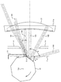
図5は、このような目的で構成される走査光学系全体(但し、レーザー光源11及びシリンドリカルレンズ12を除く)の副走査断面を示す光学構成図である。ポリゴンミラー13の各反射面に対して、各色成分に対応した4本のレーザー光束は、副走査方向において、主走査断面Pに関して二本ずつ面対称となるように傾斜した4つの方向から、夫々、同一の偏向点へ向けて入射する。その結果、図5に示されるように、ポリゴンミラー13の各反射面によって反射された各色成分に対応した4本のレーザー光束は、主走査断面Pに関して二本ずつ面対称となるように、偏向点から放射状に拡がって進行し、共通の走査レンズ21を透過した後に、夫々に対応した像面湾曲補正レンズ22を透過して、夫々に対応した感光ドラム60に照射される。従って、ポリゴンミラー13の一つの反射面による一回の偏向によって、4つの感光ドラム60に対して同時に走査を行うことができる。
【0025】
なお、走査光学系10のユニットサイズをできるだけ小型化するために、図5に示すように、ポリゴンミラー13によって偏向された4本のレーザー光束の光路が、夫々、2枚の折返しミラー23,24(ポリゴンミラー13から最も遠い感光ドラム60に入射するレーザー光束については1枚の折返しミラー23)によって折り曲げられている。この際、各fθレンズ20を透過するレーザー光束の波長は同一であるので、各折返しミラー23,24の配置位置は、各fθレンズ20の走査レンズ21から像面湾曲補正レンズ22までの光路長が互いに等しくなって各fθレンズ20が互いに同一の光学特性を奏することができるよう、夫々調整されている。
【0026】
各感光ドラム60は、互いに同じ大きさの円柱形状の外形を有するように形成されており、各像面湾曲補正レンズ22の光束射出側において、各像面湾曲補正レンズ22から等距離の位置に、夫々配置されている。
【0027】
以上のように構成される走査光学系10が内部に組み付けられているカラーレーザープリンターは、各感光ドラム60を所定の回転角速度で回転させるとともに、入力される画像情報に従ってオンオフ変調した各色成分毎のレーザー光束を、各感光ドラム60bの感光面S上で繰り返し走査させることにより、複数の線状の軌跡(走査線)からなる二次元状の静電潜像を各感光面S上に描画する。そして、カラーレーザープリンターは、各感光ドラム60上に描画された静電潜像に帯電トナーを静電的に吸着させてトナー像を形成し、そのトナー像を印刷用紙に転写させる。このとき、カラーレーザープリンターは、各感光ドラム60上の走査線が印刷用紙の同一線上に重なるように印刷用紙を搬送し、画像情報に基づくカラー画像を印刷用紙に印刷する。
【0028】
次に、本実施形態の走査光学系10において、個々の色成分に対応するレーザー光束の一部が各レンズ21,22のレンズ面にて正反射することによって生ずるゴースト光が、他のレーザー光束の光路に入らないようにするための具体的構成を、説明する。
【0029】
図2は、ポリゴンミラー13から走査レンズ21までの間における機械的構成を拡大して示す図である。この図2に示されるように、走査レンズ21は、ホルダ21aによって図示せぬケーシングに固定されている。
【0030】
また、図2において、100は、シリンドリカルレンズ12を透過してポリゴンミラー13の各反射面に入射するレーザー光束のビーム軸を示し、101は、ポリゴンミラー13の一反射面による走査開始時における正規光(当該反射面によって反射されたレーザー光束)のビーム軸を示し、102は、ポリゴンミラー13の一反射面による走査終了時における正規光(当該反射面によって反射されたレーザー光束)のビーム軸を示す。なお、本実施例においては、ポリゴンミラー13が図2における時計方向に回転するために、正規光が101から102へ走査されるが、ポリゴンミラー13の回転方向が逆であれば、正規光は102から101へ走査されることになる。
【0031】
また、図2において、104は、本実施形態において他のレーザー光束の光路への進入を防止すべき対象ゴースト光(fθレンズ20を構成する何れかのレンズ21,22における何れかのレンズ面によって正反射したレーザー光束)を示し、105は、ポリゴンミラー13の隣接面(即ち、正規光103を反射させた反射面[正規光反射面]に対してレーザー光束100の入射側とは逆側に隣接する反射面)によって反射された対象ゴースト光のビーム軸を示し、103は、対象ゴースト光の元になった正規光のビーム軸を示す。つまり、図2は、上述したように定義した偏向点とポリゴンミラー13の反射面(正規光反射面)の中心とが一致しているために正規光103がfθレンズ20(走査レンズ21)の光軸上に反射され、対象ゴースト光104がfθレンズ20(走査レンズ21)の光軸と略平行に進行してポリゴンミラー13における隣接面に入射する状態を示している。なお、実際には、ゴースト光104は、光軸と平行な方向からやや図上左上に傾くが、ゴースト光を反射させるレンズ面がポリゴンミラー13から非常に遠い場所にある場合における極限状態を想定しているので、光軸と略平行となっている。
【0032】
図2においては、αは、ポリゴンミラーの正規光反射面に入射するレーザー光束とfθレンズ20(走査レンズ21)の光軸とがなす角度,即ち、偏向角である。また、βは、fθレンズ20(走査レンズ21)の光軸に直交するとともに、正規光反射面と隣接面との間の頂点Qを通る仮想平面Tと隣接面とがなす角度である。これら角度αと角度βとの間には、ポリゴンミラー13の反射面の面数をNとして、幾何学的に、下記式(2)によって示される関係がある。
【0033】
β=π−α/2−(N−2)π/N ……(2)
いま、対象ゴースト光104がfθレンズ20(走査レンズ21)の光軸と平行に進行し、ポリゴンミラー13の隣接面において頂点Qに接するように入射したとする。その際に当該隣接面によって反射されたゴースト光105がfθレンズ20(走査レンズ21)の光軸に対してなす角度γは、幾何学的に、角度βの倍である。従って、下記式(3)が成立する。
【0034】
γ=2π−α−2(N−2)π/N ……(3)
図2においては、頂点Qを通ってfθレンズ20(走査レンズ21)の光軸に対して角度γをなす線と、レーザー光束100の入射側とは逆側の走査端における正規光101の光路(最大走査角の上光線)と、ポリゴンミラー13の正規光反射面とによって囲まれる空間が、ハッチングによって示されている。このハッチングされた空間は、正規光101〜102の走査範囲外であるとともにポリゴンミラー13の隣接面によって反射される対象ゴースト光の光路よりも光軸側である空間である。そのため、このハッチングされた空間内にその先端縁が存在するとともに前記正規光101〜102の走査範囲外を遮光するように、矩形板形状を有する遮光板15が、fθレンズ20(走査レンズ21)の光軸に対して垂直に設置されている。従って、図2の状態においては、正規光101〜102が遮光板15によって遮光されることなく、隣接面によって反射された対象ゴースト光104が遮光板15によって遮光されるので、実際には、この対象ゴースト光104は、走査レンズ21には再入射しない。
【0035】
なお、図2において、14は、正規光の走査範囲101〜102の外側において迷光を遮光するために図示せぬケーシングに形成された遮光壁である。
【0036】
図3は、図2の状態よりもポリゴンミラー13が時計方向に回転した状態を示している。この状態では、ポリゴンミラー13の正規光反射面によって反射される正規光が、fθレンズ20(走査レンズ21)の光軸と平行な方向よりも、レーザー光束100の入射側へ傾くので、対象ゴースト光104は、ポリゴンミラー13の隣接面ではなく、正規光反射面に入射する。従って、この正規光反射面にて反射された後における対象ゴースト光は、正規光の走査範囲101〜102の外側へ進行するので、走査レンズ21に再入射することはない。
【0037】
図4は、逆に、図2の状態よりもポリゴンミラー13が反時計方向に戻った状態を示している。この状態では、ポリゴンミラー13の正規光反射面によって反射される正規光が、fθレンズ20(走査レンズ21)の光軸と平行な方向よりも、レーザー光束100の入射側とは逆側へ傾くので、対象ゴースト光104は、走査レンズ21の前面における図2に示す位置よりも主走査方向において高い位置からポリゴンミラー13の隣接面に向けて射出される。従って、この隣接面にて反射された後における対象ゴースト光は、完全に遮光板13によって遮光されるので、走査レンズ21に再入射することはない。
【0038】
以上に示したように、本実施形態によれば、fθレンズ20(走査レンズ21)の光軸と平行に戻ってポリゴンミラー13の隣接面によって反射された後の対象ゴースト光104の光路とレーザー光束100の入射側とは逆側の走査端における正規光101の光路とによって囲まれる空間内にその先端が存在するとともに正規光101〜102の走査範囲外を遮光するように、矩形板形状を有する遮光板15をfθレンズ20(走査レンズ21)の光軸に対して垂直に設置するという簡単な構成によって、対象ゴースト光がfθレンズ20(走査レンズ21)に再入射することが防止される。従って、対象ゴースト光が、その元になった正規光に対して主走査断面Pに関して面対称となるように進行する他の正規光の光路に進入することがない。従って、マルチビーム走査光学系によって最終的に形成されるカラー画像の品質が劣化することが、防止される。
【0039】
【発明の効果】
以上に説明したように、本発明のマルチビーム走査光学系によれば、何れかの正規光の一部が何れかのレンズ面にて正反射されることによって生じたゴースト光がポリゴンミラーの各反射面によって反射されて他の正規光の光路に進入することを、簡単な構成によって防止することができる。
【図面の簡単な説明】
【図1】 本発明の一実施形態によるマルチビーム走査光学系の基本構成を展開して示す光学構成図
【図2】 走査レンズの光軸と平行に対象ゴースト光が進行して隣接面に入射する状態におけるポリゴンミラーから走査レンズまでの間の機械構成を示す拡大図
【図3】 図2の状態よりもポリゴンミラーが時計方向に回転した状態におけるポリゴンミラーから走査レンズまでの間の機械構成を示す拡大図
【図4】 図2の状態よりもポリゴンミラーが反時計方向に戻った状態におけるポリゴンミラーから走査レンズまでの間の機械構成を示す拡大図
【図5】 ポリゴンミラーから各感光ドラムまでの走査光学系の副走査方向における光学構成を示す光学構成図
【符号の説明】
10 走査光学系
11 レーザー光源
12 シリンドリカルレンズ
13 ポリゴンミラー
20 fθレンズ
21 走査レンズ
22 像面湾曲補正レンズ
60 感光ドラム
S 感光面[0001]
BACKGROUND OF THE INVENTION
According to the present invention, a laser beam emitted from a light source is deflected by being reflected by a reflecting surface of a polygon mirror that rotates in a certain direction, and is converged by being transmitted through an imaging optical system. It relates to a scanning optical system that scans above.
[0002]
[Prior art]
The scanning optical system is used to scan a photosensitive surface such as a photosensitive drum with a modulated beam in, for example, an electrophotographic laser beam printer, digital copy, or laser fax.
[0003]
Specifically, the scanning optical system scans the laser beam, which is on / off modulated according to the image information, with a polygon mirror, and converges the scanned laser beam as spot light on the surface to be scanned by the imaging optical system. As a result, the scanning optical system scans the spot light on the scanning target surface at a constant speed along the main scanning direction, and forms a two-dimensional image composed of a plurality of dots on the photosensitive surface of the photosensitive drum.
[0004]
By the way, in a scanning optical system, how to remove a ghost due to unnecessary reflection on the surface of each optical element is an important design matter. Such unnecessary reflection may occur, for example, on each lens surface of each lens constituting the imaging optical system. A part of a laser beam (hereinafter referred to as “regular light”) incident on any lens surface after being reflected by any reflective surface of the polygon mirror (hereinafter referred to as “regular light reflecting surface”) When the lens surface is regularly reflected as ghost light to become ghost light, the ghost light returns in a direction determined by the beam axis direction of the regular light and the incident angle with respect to the lens surface. If each reflection surface of the polygon mirror exists in the direction in which the ghost light is returned, the ghost light is reflected again by this reflection surface, passes through the imaging optical system, and enters the photosensitive surface of the photosensitive drum. End up.
[0005]
At this time, when ghost light is incident on the regular light reflecting surface, the ghost light moves on the photosensitive surface of the photosensitive drum at almost the same speed as the scanning speed of the laser beam. Since energy is distributed on the photosensitive surface, ghosting problems do not occur.
[0006]
On the other hand, when ghost light is incident on a reflection surface (hereinafter referred to as “adjacent surface”) adjacent to the regular light reflection surface of the polygon mirror, the moving speed of the ghost light is higher than the scanning speed of the laser beam. Depending on the cross-sectional shape of the lens surface reflecting the ghost light in the main scanning direction, it may be almost stopped. In this case, the energy of ghost light is accumulated only in a part in the main scanning direction on the photosensitive surface. As a result, print density unevenness (ghost) occurs in the main scanning direction. As a result, there arises a problem that the drawing performance of the camera deteriorates.
[0007]
Such a problem is that one polygon mirror simultaneously scans a plurality of laser beams for drawing on a plurality of photosensitive drums corresponding to each toner color in color printing, so-called “one polygon multi-beam scanning”. This is remarkable in the case of the “optical system”. This is because, in a general one-beam scanning optical system that scans the main scanning section, in order to prevent reflection between lens surfaces, a means for preventing the ghost by decentering the optical axis of each lens can be taken. In an optical system in which a plurality of regular light beams are symmetrical with respect to the main scanning section P, such as a “polygon multi-beam scanning optical system”, it is extremely difficult to prevent ghosts between lens surfaces.
[0008]
That is, in the “one polygon multi-beam scanning optical system”, in the sub-scanning direction parallel to the rotation axis of the polygon mirror, a virtual plane orthogonal to the rotation axis and the center of each reflecting surface (hereinafter referred to as “main scanning section”). A plurality (even number) of laser light beams are obliquely incident on the regular light reflecting surface so as to be symmetrical with respect to the surface. As a result, as shown in FIG. 5, approximately one point of the regular light reflecting surface so that the plurality of regular light reflected by the regular light reflecting surface of the
[0009]
As described above, in the “one polygon multi-beam scanning optical system”, a plurality of regular lights travel radially from substantially one point on the regular light reflecting surface so as to be symmetrical with respect to the main scanning section P. When ghost light is generated by specularly reflecting a part of any regular light on any lens surface, the ghost light follows the optical path of the original regular light in the sub-scanning direction, and the
[0010]
As a result, another color ghost having a reduced form of the image superimposed on the image of a certain color is developed on the same printing paper. Since such a ghost is generated for each color, the quality of the color image finally formed is significantly impaired.
[0011]
[Problems to be solved by the invention]
Accordingly, an object of the present invention is to make a plurality of laser light beams symmetrical with respect to each reflection surface of the polygon mirror with respect to the main scanning section orthogonal to the rotation axis of each polygon mirror and each reflection surface in the sub-scanning direction. In a multi-beam scanning optical system in which each laser beam reflected by a reflecting surface is converged on an individual photosensitive drum by a corresponding imaging optical system, a part of any regular light is any Providing a configuration that can prevent ghost light generated by regular reflection on the lens surface from being reflected by each reflective surface of the polygon mirror and entering the optical path of other regular light with a simple configuration. It is to be.
[0012]
[Means for Solving the Problems]
A multi-beam scanning optical system according to the present invention configured to solve the above-described problems has a polygonal column shape whose side surfaces are formed as reflecting surfaces, and a polygon mirror that rotates about its central axis, A plurality of light sources that emit laser beams toward one point in the vicinity of the reflecting surface so as to be plane-symmetric with respect to the main scanning section orthogonal to the central axis and the reflecting surfaces in the sub-scanning direction parallel to the central axis And in the sub-scanning direction, each laser beam reflected by the reflecting surface so as to be radially symmetric with respect to the main scanning section is converged on the photosensitive surface of the corresponding photosensitive drum, and An imaging optical system in which the optical axis forms a predetermined deflection angle α with respect to the laser beam emitted from each light source in the main scanning direction parallel to the main scanning section. In the main scanning direction, the outer edge on the side away from the light source in the scanning range of each laser beam reflected by any reflecting surface of the rotating polygon mirror, and the optical axis of the imaging optical system It passes through the position of the apex of the reflection surface reflecting each laser beam at the time of reflection upward and the adjacent surface adjacent to the side away from the light source, and the following formula with respect to the optical axis of the imaging optical system The front end of the laser beam in a space surrounded by a line forming an angle γ determined by (1) and a reflecting surface reflecting each laser beam at the time when each laser beam is reflected on the optical axis of the imaging optical system. And a light shielding plate arranged so as to shield light outside the scanning range.
[0013]
γ = 2π−α−2 (N−2) π / N (1)
N is the number of reflecting surfaces of the polygon mirror.
[0014]
When the multi-beam scanning optical system is configured in this way, each laser beam emitted from each light source and reflected by each reflecting surface of the polygon mirror is not shielded by the light shielding plate, but is reflected by any reflection Ghost light generated by specular reflection of a part of each laser beam at any lens surface when the surface reflects each laser beam on the optical axis of the imaging optical system in the main scanning direction Even if the light beam returns substantially parallel to the optical axis of the imaging optical system and is incident on a reflection surface adjacent to the reflection surface on the side away from the light source, the reflected ghost light is reliably transmitted by the light shielding plate. Shielded from light. When the reflection surface of the polygon mirror is rotated toward the light source from the rotation position at that time, the ghost light emitted from the imaging optical system is incident not on the adjacent surface but on the reflection surface reflecting each laser beam. Therefore, the reflected light does not enter the imaging optical system. On the other hand, when the reflecting surface of the polygon mirror rotates in the reverse direction relative to the rotational position at the above time, the ghost light emitted from the imaging optical system comes from the optical axis of the imaging optical system as it approaches the polygon mirror. Tilt away. Therefore, even if the ghost light is reflected by the adjacent surface, the reflected light is reliably shielded by the light shielding plate.
[0015]
DETAILED DESCRIPTION OF THE INVENTION
Hereinafter, a scanning device according to an embodiment of the scanning optical system of the present invention will be described with reference to the drawings.
[0016]
FIG. 1 is an optical configuration diagram showing a developed state of the basic configuration of the scanning optical system according to the present embodiment. As shown in FIG. 1, the scanning optical system 10 includes a
[0017]
The parallel laser beam emitted from the
[0018]
The laser beam emitted from the
[0019]
The
[0020]
The lens surfaces of the
[0021]
Further, a surface including the optical axis of the
[0022]
The photosensitive surface S is an outer peripheral surface of the
[0023]
Of the basic configuration of the scanning optical system 10 described above, the parts other than the
[0024]
FIG. 5 is an optical configuration diagram showing a sub-scanning section of the entire scanning optical system (excluding the
[0025]
In order to make the unit size of the scanning optical system 10 as small as possible, as shown in FIG. 5, the optical paths of the four laser beams deflected by the
[0026]
Each
[0027]
In the color laser printer in which the scanning optical system 10 configured as described above is assembled, each
[0028]
Next, in the scanning optical system 10 of the present embodiment, ghost light generated by specularly reflecting a part of the laser beam corresponding to each color component on the lens surfaces of the
[0029]
FIG. 2 is an enlarged view showing a mechanical configuration between the
[0030]
In FIG. 2,
[0031]
In FIG. 2,
[0032]
In FIG. 2, α is an angle formed by the laser beam incident on the regular light reflecting surface of the polygon mirror and the optical axis of the fθ lens 20 (scanning lens 21), that is, a deflection angle. Further, β is an angle formed between the virtual plane T passing through the vertex Q between the normal light reflecting surface and the adjacent surface and the adjacent surface while being orthogonal to the optical axis of the fθ lens 20 (scanning lens 21). Between these angles α and β, there is a geometric relationship represented by the following equation (2), where N is the number of reflecting surfaces of the
[0033]
β = π−α / 2− (N−2) π / N (2)
Now, it is assumed that the target ghost light 104 travels parallel to the optical axis of the fθ lens 20 (scanning lens 21) and is incident on the adjacent surface of the
[0034]
γ = 2π−α−2 (N−2) π / N (3)
In FIG. 2, the line that forms an angle γ with respect to the optical axis of the fθ lens 20 (scanning lens 21) through the apex Q, and the optical path of the
[0035]
In FIG. 2,
[0036]
FIG. 3 shows a state where the
[0037]
FIG. 4 shows a state where the
[0038]
As described above, according to the present embodiment, the optical path and laser of the target ghost light 104 after being reflected by the adjacent surface of the
[0039]
【The invention's effect】
As described above, according to the multi-beam scanning optical system of the present invention, the ghost light generated by specular reflection of a part of any regular light on any lens surface is reflected on each polygon mirror. It is possible to prevent the light from being reflected by the reflecting surface and entering the optical path of other regular light with a simple configuration.
[Brief description of the drawings]
FIG. 1 is an optical configuration diagram showing a basic configuration of a multi-beam scanning optical system according to an embodiment of the present invention. FIG. 2 is a target ghost light traveling parallel to the optical axis of a scanning lens and entering an adjacent surface. FIG. 3 is an enlarged view showing a mechanical configuration from the polygon mirror to the scanning lens in a state where the polygon mirror is rotated. Enlarged view showing FIG. 4 Enlarged view showing a mechanical configuration from the polygon mirror to the scanning lens in a state where the polygon mirror returns counterclockwise from the state of FIG. 2. FIG. 5 From the polygon mirror to each photosensitive drum Optical configuration diagram showing the optical configuration of the scanning optical system in the sub-scanning direction
DESCRIPTION OF SYMBOLS 10 Scan
Claims (2)
前記中心軸と平行な副走査方向において、前記中心軸及び前記各反射面に直交する主走査断面に関して面対称となるように、前記反射面近傍の一点に向けて夫々レーザー光束を発する複数の光源と、
副走査方向において、前記主走査断面に関して面対称となって放射状に拡がるように前記反射面によって反射された各レーザー光束を、夫々に対応する感光ドラムの感光面上に収束させるとともに、前記主走査断面と平行な主走査方向において、前記各光源から発するレーザー光束に対してその光軸が所定の偏向角αをなす結像光学系と、
主走査方向において、回転中のポリゴンミラーの何れかの反射面によって反射される各レーザー光束の走査範囲における前記光源から離れた側の外縁と、各レーザー光束を前記結像光学系の光軸上に反射させる時点における当該各レーザー光束を反射させている反射面と前記光源から離れた側に隣接する隣接面との頂点の位置を通るとともに前記結像光学系の光軸に対して下記式(1)によって定まる角度γをなす線と、各レーザー光束を前記結像光学系の光軸上に反射させる時点における当該各レーザー光束を反射させている反射面とによって囲まれる空間内にその先端が存在するとともに、前記走査範囲外を遮光するように配置された遮光板とを備えることを特徴とするマルチビーム走査光学系。
γ=2π−α−2(N−2)π/N ……(1)
但し、Nは前記ポリゴンミラーの反射面数A polygon mirror that has a polygonal prism shape whose side surfaces are each formed as a reflecting surface and rotates about its central axis;
A plurality of light sources that emit laser beams toward one point in the vicinity of the reflecting surface so as to be plane-symmetric with respect to the main scanning section orthogonal to the central axis and the reflecting surfaces in the sub-scanning direction parallel to the central axis When,
In the sub-scanning direction, each laser beam reflected by the reflecting surface is converged on the photosensitive surface of the corresponding photosensitive drum so as to be radially symmetric with respect to the main scanning section in the sub-scanning direction. An imaging optical system whose optical axis forms a predetermined deflection angle α with respect to the laser beam emitted from each light source in the main scanning direction parallel to the cross section;
In the main scanning direction, the outer edge on the side away from the light source in the scanning range of each laser beam reflected by any reflecting surface of the rotating polygon mirror, and each laser beam on the optical axis of the imaging optical system And passes through the position of the apex of the reflection surface reflecting each laser beam at the time of reflection to the adjacent surface adjacent to the side away from the light source, and the following equation (with respect to the optical axis of the imaging optical system) 1), the tip of the laser beam is reflected in a space surrounded by a line that forms an angle γ determined by 1) and a reflection surface that reflects each laser beam on the optical axis of the imaging optical system. A multi-beam scanning optical system comprising: a light-shielding plate that exists and is disposed so as to shield light outside the scanning range.
γ = 2π−α−2 (N−2) π / N (1)
Where N is the number of reflecting surfaces of the polygon mirror
ことを特徴とする請求項1記載のマルチビーム走査光学系。The multi-beam scanning optical system according to claim 1, wherein the light shielding plate is a rectangular plate.
Priority Applications (2)
| Application Number | Priority Date | Filing Date | Title |
|---|---|---|---|
| JP2002189887A JP4133036B2 (en) | 2002-06-28 | 2002-06-28 | Multi-beam scanning optical system |
| US10/606,221 US6873466B2 (en) | 2002-06-28 | 2003-06-26 | Scanning optical system |
Applications Claiming Priority (1)
| Application Number | Priority Date | Filing Date | Title |
|---|---|---|---|
| JP2002189887A JP4133036B2 (en) | 2002-06-28 | 2002-06-28 | Multi-beam scanning optical system |
Publications (3)
| Publication Number | Publication Date |
|---|---|
| JP2004029671A JP2004029671A (en) | 2004-01-29 |
| JP2004029671A5 JP2004029671A5 (en) | 2005-09-02 |
| JP4133036B2 true JP4133036B2 (en) | 2008-08-13 |
Family
ID=31184175
Family Applications (1)
| Application Number | Title | Priority Date | Filing Date |
|---|---|---|---|
| JP2002189887A Expired - Fee Related JP4133036B2 (en) | 2002-06-28 | 2002-06-28 | Multi-beam scanning optical system |
Country Status (2)
| Country | Link |
|---|---|
| US (1) | US6873466B2 (en) |
| JP (1) | JP4133036B2 (en) |
Families Citing this family (11)
| Publication number | Priority date | Publication date | Assignee | Title |
|---|---|---|---|---|
| JP4380445B2 (en) * | 2004-07-22 | 2009-12-09 | ブラザー工業株式会社 | Image forming apparatus and scanning unit |
| JP4925623B2 (en) | 2004-09-13 | 2012-05-09 | 株式会社リコー | Optical scanning apparatus and image forming apparatus |
| JP4654350B2 (en) * | 2004-12-13 | 2011-03-16 | Hoya株式会社 | Scanning optical system |
| JP2006215351A (en) * | 2005-02-04 | 2006-08-17 | Ricoh Printing Systems Ltd | Optical scanner and image forming apparatus |
| US7271941B2 (en) * | 2005-03-07 | 2007-09-18 | Lexmark International, Inc. | Laser scanning unit including a shield |
| JP2007010797A (en) * | 2005-06-28 | 2007-01-18 | Ricoh Co Ltd | Optical scanner and image forming apparatus |
| JP4786261B2 (en) * | 2005-09-06 | 2011-10-05 | 株式会社リコー | Optical scanning apparatus and image forming apparatus |
| US7554569B2 (en) * | 2006-01-18 | 2009-06-30 | Hoya Corporation | Light scanning device |
| JP5026141B2 (en) * | 2007-05-02 | 2012-09-12 | 株式会社リコー | Image forming apparatus and image forming method |
| JP2010026115A (en) * | 2008-07-17 | 2010-02-04 | Kyocera Mita Corp | Scan optical device and image forming apparatus provided with it |
| JP2012159528A (en) * | 2011-01-28 | 2012-08-23 | Kyocera Document Solutions Inc | Optical scanning device and image forming device |
Family Cites Families (7)
| Publication number | Priority date | Publication date | Assignee | Title |
|---|---|---|---|---|
| US5181137A (en) * | 1988-08-24 | 1993-01-19 | Canon Kabushiki Kaisha | Light scanning apparatus |
| JPH06160743A (en) | 1992-11-17 | 1994-06-07 | Konica Corp | Laser beam scanner |
| JP3257646B2 (en) * | 1993-04-05 | 2002-02-18 | 富士ゼロックス株式会社 | Laser beam printer |
| JP3598686B2 (en) | 1996-11-01 | 2004-12-08 | 富士ゼロックス株式会社 | Optical scanning device |
| JP2001033721A (en) | 1999-07-19 | 2001-02-09 | Asahi Optical Co Ltd | Scanning optical device |
| JP3673709B2 (en) * | 1999-11-09 | 2005-07-20 | キヤノン株式会社 | Optical scanning apparatus and image forming apparatus |
| JP4439141B2 (en) | 2001-06-20 | 2010-03-24 | Hoya株式会社 | Scanning optical system |
-
2002
- 2002-06-28 JP JP2002189887A patent/JP4133036B2/en not_active Expired - Fee Related
-
2003
- 2003-06-26 US US10/606,221 patent/US6873466B2/en not_active Expired - Fee Related
Also Published As
| Publication number | Publication date |
|---|---|
| US20040036939A1 (en) | 2004-02-26 |
| JP2004029671A (en) | 2004-01-29 |
| US6873466B2 (en) | 2005-03-29 |
Similar Documents
| Publication | Publication Date | Title |
|---|---|---|
| JPH08220440A (en) | Optical scanning device, image forming device and image reading device | |
| JP2018132638A (en) | Optical scanner, image forming apparatus, and housing | |
| JP4133036B2 (en) | Multi-beam scanning optical system | |
| JP5333070B2 (en) | Optical scanning apparatus and image forming apparatus | |
| JP4430855B2 (en) | Scanning optical system | |
| JP2009192680A (en) | Optical scanning device and image forming apparatus using the same | |
| JP4171284B2 (en) | Scanning optical system | |
| JP4593886B2 (en) | Optical scanning device and image forming apparatus using the same | |
| JP2002182143A (en) | Optical scanner, multibeam scanner and image forming device | |
| JP4294913B2 (en) | Optical scanning apparatus and image forming apparatus | |
| US8872874B2 (en) | Light scanning unit and electrophotographic image forming apparatus using the same | |
| JP2005091966A (en) | Optical scanner and color image forming apparatus using it | |
| JP3747668B2 (en) | Optical scanning device | |
| JP4225021B2 (en) | Multi-beam laser emitting unit and image forming apparatus | |
| JP5877818B2 (en) | Optical scanning apparatus and image forming apparatus | |
| JP2004226864A (en) | Optical scanner and image forming device | |
| JP4706628B2 (en) | Optical scanning device | |
| JP2024006602A (en) | Optical scanner and image forming apparatus | |
| JP5303346B2 (en) | Optical scanning apparatus and image forming apparatus having the same | |
| JP2999853B2 (en) | Optical scanning device | |
| JP4744117B2 (en) | Optical scanning apparatus and image forming apparatus | |
| JP2004102268A (en) | Method for producing scanning optical system | |
| JP2004020692A (en) | Scanner and image forming apparatus using the same | |
| JP4374493B2 (en) | Optical scanning apparatus and image forming apparatus | |
| JP4017576B2 (en) | Optical scanning apparatus and image forming apparatus |
Legal Events
| Date | Code | Title | Description |
|---|---|---|---|
| A521 | Written amendment |
Free format text: JAPANESE INTERMEDIATE CODE: A523 Effective date: 20050303 |
|
| A621 | Written request for application examination |
Free format text: JAPANESE INTERMEDIATE CODE: A621 Effective date: 20050303 |
|
| A977 | Report on retrieval |
Free format text: JAPANESE INTERMEDIATE CODE: A971007 Effective date: 20080227 |
|
| A131 | Notification of reasons for refusal |
Free format text: JAPANESE INTERMEDIATE CODE: A131 Effective date: 20080304 |
|
| A711 | Notification of change in applicant |
Free format text: JAPANESE INTERMEDIATE CODE: A712 Effective date: 20080430 |
|
| A521 | Written amendment |
Free format text: JAPANESE INTERMEDIATE CODE: A523 Effective date: 20080507 |
|
| TRDD | Decision of grant or rejection written | ||
| A01 | Written decision to grant a patent or to grant a registration (utility model) |
Free format text: JAPANESE INTERMEDIATE CODE: A01 Effective date: 20080527 |
|
| A01 | Written decision to grant a patent or to grant a registration (utility model) |
Free format text: JAPANESE INTERMEDIATE CODE: A01 |
|
| A61 | First payment of annual fees (during grant procedure) |
Free format text: JAPANESE INTERMEDIATE CODE: A61 Effective date: 20080602 |
|
| FPAY | Renewal fee payment (event date is renewal date of database) |
Free format text: PAYMENT UNTIL: 20110606 Year of fee payment: 3 |
|
| R150 | Certificate of patent or registration of utility model |
Free format text: JAPANESE INTERMEDIATE CODE: R150 |
|
| FPAY | Renewal fee payment (event date is renewal date of database) |
Free format text: PAYMENT UNTIL: 20120606 Year of fee payment: 4 |
|
| FPAY | Renewal fee payment (event date is renewal date of database) |
Free format text: PAYMENT UNTIL: 20130606 Year of fee payment: 5 |
|
| FPAY | Renewal fee payment (event date is renewal date of database) |
Free format text: PAYMENT UNTIL: 20140606 Year of fee payment: 6 |
|
| LAPS | Cancellation because of no payment of annual fees |