EP1099965A2 - Optical fiber delay lines for digital signal processing - Google Patents
Optical fiber delay lines for digital signal processing Download PDFInfo
- Publication number
- EP1099965A2 EP1099965A2 EP00309580A EP00309580A EP1099965A2 EP 1099965 A2 EP1099965 A2 EP 1099965A2 EP 00309580 A EP00309580 A EP 00309580A EP 00309580 A EP00309580 A EP 00309580A EP 1099965 A2 EP1099965 A2 EP 1099965A2
- Authority
- EP
- European Patent Office
- Prior art keywords
- optical
- segments
- delay line
- input
- output
- Prior art date
- Legal status (The legal status is an assumption and is not a legal conclusion. Google has not performed a legal analysis and makes no representation as to the accuracy of the status listed.)
- Withdrawn
Links
Images



Classifications
-
- G—PHYSICS
- G02—OPTICS
- G02B—OPTICAL ELEMENTS, SYSTEMS OR APPARATUS
- G02B6/00—Light guides; Structural details of arrangements comprising light guides and other optical elements, e.g. couplings
- G02B6/24—Coupling light guides
- G02B6/26—Optical coupling means
- G02B6/28—Optical coupling means having data bus means, i.e. plural waveguides interconnected and providing an inherently bidirectional system by mixing and splitting signals
- G02B6/2804—Optical coupling means having data bus means, i.e. plural waveguides interconnected and providing an inherently bidirectional system by mixing and splitting signals forming multipart couplers without wavelength selective elements, e.g. "T" couplers, star couplers
- G02B6/2861—Optical coupling means having data bus means, i.e. plural waveguides interconnected and providing an inherently bidirectional system by mixing and splitting signals forming multipart couplers without wavelength selective elements, e.g. "T" couplers, star couplers using fibre optic delay lines and optical elements associated with them, e.g. for use in signal processing, e.g. filtering
-
- G—PHYSICS
- G02—OPTICS
- G02B—OPTICAL ELEMENTS, SYSTEMS OR APPARATUS
- G02B6/00—Light guides; Structural details of arrangements comprising light guides and other optical elements, e.g. couplings
- G02B6/24—Coupling light guides
- G02B6/36—Mechanical coupling means
- G02B6/3608—Fibre wiring boards, i.e. where fibres are embedded or attached in a pattern on or to a substrate, e.g. flexible sheets
-
- G—PHYSICS
- G02—OPTICS
- G02B—OPTICAL ELEMENTS, SYSTEMS OR APPARATUS
- G02B6/00—Light guides; Structural details of arrangements comprising light guides and other optical elements, e.g. couplings
- G02B6/44—Mechanical structures for providing tensile strength and external protection for fibres, e.g. optical transmission cables
- G02B6/4439—Auxiliary devices
- G02B6/444—Systems or boxes with surplus lengths
Definitions
- This invention relates to optical fiber-based digital delay lines. More specifically, it relates to a multi-fiber digital delay line incorporating nested optical fibers affixed to a substrate in a single physical plane.
- WDM wave division multiplexed
- DWDM dense wave division multiplexed
- Optical delay lines may be formed using a variety of optical technologies (see, e.g., Kenneth P. Jackson et al., "Optical Fiber Delay-Line Signal Processing," IEEE Transactions On Microwave Theory And Techniques, Vol. MTT-33, No. 3, March 1985, pp193, 194).
- Optical fiber delay lines have proven to be attractive due to their relatively low loss and low dispersion characteristics.
- Typical optical fiber configurations include recirculating delay lines, multi-tap delay lines and multi-fiber delay lines.
- a recirculating delay line incorporates a fiber which partially closes upon itself (for example, by means of an optical coupler) so that signals introduced at one end of the delay line recirculate around the loop to be output with each transit cycle.
- Non-recirculating optical fiber delay lines such as multi-tap and multi-fiber delay lines produce only a single output signal at each output port in response to each input signal.
- the multi-tap structure consists of a fiber with taps distributed along its length, each tap being capable of providing a signal output.
- the output signals from each tap may be collected and output by an optical combiner. Relative delays among the output signals are controlled by the relative placement of taps along the fiber.
- an optical signal is split and provided as input to two or more optical fibers of varying length (see, e.g., U.S. patent 5,703,708, issuing to Das et al. on December 30, 1997).
- the optical signals on each fiber's output are collected and output by an optical combiner.
- the optical signal in the shorter fiber appears at the combiner at a point earlier in time than the optical signal in the longer fiber. Accordingly, delay may be controlled among the multiple fibers by adjusting the relative differences in length among the fibers.
- Longer fibers can be packaged adjacent to shorter fibers by winding at least of segment of the added differential length of the longer fiber onto a spool.
- the spool helps to lessen the space required, it introduces several difficulties. Variations in the physical length and tension of the optical fiber that result as it is wound onto the spool can cause variations in the effective optical length of the fiber. In addition, optical length may vary with movement of the fiber on the spool.
- Such variations may be adjusted, for example, by incorporating a heater in the center of the spool to establish a stable thermal profile for the fiber on the spool.
- variations in the geometry of the spool and in the positioning of the fiber on the spool can make it difficult to establish stability in the thermal profile.
- a multi-fiber optical delay line incorporates a plurality of optical fibers nestedly positioned so that the individual ones of the plurality of optical fibers are collectively positioned in a single plane.
- Input ends for each of the plurality of optical fibers are connected to an optical splitter, which thereby provides a copy of an input signal to each of the plurality of optical fibers substantially simultaneously.
- Each of the plurality of optical fibers has a unique, predetermined length, causing each copy of the input signal that travels over an associated one of the plurality of fibers to arrive at an output end of the associated fiber at the end of a unique interval in time.
- the nestedly planar structure and geometry of the delay line allows the optical length of each of the plurality of optical fibers to be precisely controlled.
- each of the plurality of optical fibers includes an input segment and an output segment joined by a u-shaped connecting segment.
- the input segments are substantially parallel, equal in length and proximately positioned so that input ends of the input segments all lie substantially near a straight line that is perpendicular to the input segments.
- the output segments are substantially parallel, equal in length and proximately positioned so that output ends of the output segments all lie substantially near a straight line substantially perpendicular to the output segments.
- Each of the u-shaped connecting segments of the plurality of optical fibers has a unique, predetermined length. To maintain a planar positioning, each of the plurality of optical fibers is affixed to a planar surface of a substrate.
- the output ends of the plurality of optical fibers are each further coupled to one of a plurality of input ports in an optical combiner, such that the optical combiner superimposes received signal copies from the plurality of optical fibers to produce a single optical signal output.
- a planar heater is attached to a second planar surface of the substrate so that a temperature profile may be established and stabilized in the plurality of optical fibers.
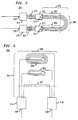
- FIG. 1 shows the structure of a prior art optical multiplexer incorporating a multi-fiber optical delay line 100 (see, e.g, U.S. patent 5,703,708, issuing to Das et al. on December 30, 1997).
- An optical signal is provided to an optical splitter 118, which produces copies of the signal on four separate fiber signal paths 103, 105, 107 and 109, which are associated with modulators 102, 104, 106 and 108, respectively.
- Modulated signals are output by the modulators 102, 104, 106 and 108 over signal paths 113, 115, 117 and 109, respectively, and are coupled to inputs of optical combiner 110.
- Optical combiner 110 superimposes signals provided over the paths 113, 115, 117 and 119 to produce a combined optical signal 111.
- optical delay lines 112, 114 and 116 are placed in the fiber signal paths associated with modulators 104, 106, and 108, respectively.
- Delay lines 112, 114 and 116 produce signal delays T, 2T and 3T, respectively, where the delay T corresponds to a desired time period.
- Signal delays T, 2T and 3T are produced by selecting optical delay lines 112, 114 and 116 with predetermined lengths in the ratio of 1:2:3, respectively.
- signals arriving simultaneously on the signal paths associated with modulators 104, 106 and 108 begin to appear at the output 110 one, two and three time periods, respectively, after the appearance at the output 110 of the signal on the signal path associated with the modulator 102.
- the signals on the signal paths associated with the modulators 102, 104, 106 and 108 are accordingly time-division multiplexed onto the single path output 110.
- delay lines 112, 114 and 116 are each produced by winding an optical fiber 220 of appropriate length onto a cylindrical spool 222. Variations in the physical length and tension of the optical fiber wound onto the spool 222 cause variations in the effective optical length of the fiber 220.
- the effective optical length for example, determines the time required for an optical signal of a given frequency to travel through the fiber 220.
- a heating element 224 is positioned on the central axis of the cylindrical spool 222 to enable the effective optical length of the optical fiber 220 to be thermally tuned and stabilized.
- the delay line 100 of FIG. 1 may be ineffective to control, for example, optical lengths in high-speed digital applications where the differences in optical length between delay lines 112, 114 and 116 of FIG. 1 are quite small.
- this configuration will be ineffective for thermally tuning segments of optical fibers associated with the delay lines 112, 114 and 116 that are not wound onto the spool 222 of FIG. 2 (for example, a fiber segment that comes off of the spool 222 in order to provide optical connection to the modulator 102 of FIG. 1).
- optical fibers 302 of delay line 300 are nestedly positioned in a single plane.
- Each fiber includes an input segment 304 and an output segment 306 joined by a u-shaped connecting segment 308.
- the input segments 304 are substantially parallel, equal in length and proximately positioned so that input ends 310 of the input segments all lie substantially near a straight line that is perpendicular to the input segments.
- the output segments 306 are substantially parallel, equal in length and proximately positioned so that output ends 312 of the output segments all lie substantially near a straight line substantially to the output segments 306.
- each of the u-shaped connecting segments 308 of the plurality of optical fibers 302 has a unique, predetermined length.
- the input ends 310 of the plurality of optical fibers are further individually coupled to output fibers 316 of an optical splitter 314 via a mass fiber interconnection 322.
- Optical splitters are well-known in the art and are available commercially from a number of suppliers including, for example, Photonic Integration Research, Inc. and Sumitomo Electric Lightwave Corp.
- Mass fiber interconnection methods are well-known in the art. A preferred method for mass fiber interconnection is mass fusion splicing, which may be performed using equipment available from a variety of commercial vendors including Sumitomo Electric Lightwave Corp. and Fujikura Limited.
- An optical signal for example, amplitude modulated as a digital bit stream, is provided at an input 326 of the splitter 314.
- the optical splitter 314 Via output port fibers 316 that are formed, for example, in equal lengths in a ribbon, the optical splitter 314 provides copies of a single input signal substantially simultaneously to each of the plurality of input segments 304 at the mass fiber interconnection 322. The copies travel through input segments 304, connecting segments 308 and output segments 306 until they reach input port fibers 320 of an optical combiner 318 via mass fiber connection 324.
- Input port fibers 320 are formed, for example, in equal lengths in a ribbon so that optical signals arriving at output ends 312 of optical fibers 302 may arrive in an equivalent time sequence at optical combiner 318.
- Optical combiner 318 combines the received signals into a single signal provided at combiner output 328.
- the output 328 may typically be interconnected with a conventional photodetector to detect the presence of the combined optical signal.
- photodetectors are commercially available, for example, from Lucent Technologies Inc.
- each of the u-shaped connecting segments 308 of the plurality of optical fibers 302 has a unique, predetermined length, optical signal copies introduced into the optical fibers 302 at input ends 310 will each travel along an optical fiber 302 of unique length to arrive at an associated output end 312 of the fiber 302 at a unique time.
- ⁇ T R n c * ( L L - L S )/c
- n c the refractive index of the core of the fiber
- c the speed of light in a vacuum
- optical fibers 302 By maintaining the optical fibers 302 in a single geometrical plane with input segments 304 and output segments 306 each including fiber segments of equal length positioned proximately, individual fiber lengths for the optical fibers 302 may be more easily controlled. Control of fiber length is extremely important in high-speed, bit-selective applications of the delay line in which differential lengths L L - L S may be extremely small (for example, as small as as five millimeters in 40 gigabit per second digital applications).
- FIG. 4A illustrates a second embodiment of the present invention.
- optical fibers 402 of delay line 400 are nestedly positioned, substantially in a single plane.
- Input segments 404 and output segments 406 each contain fiber lengths that are substantially parallel, equal in length and proximately positioned.
- the fiber lengths in the connecting segments 408 of FIG. 4 further incorporate coil segments 409.
- Coil segments 409 lie substantially in the single plane defined by the optical fibers 402, and provide a compact means for increasing the lengths of the optical fibers 402 over the lengths of the optical fibers 302 of FIG. 3.
- This embodiment may be important in optical buffering applications where an absolute time of delay ⁇ T A is of importance, as measured from the time that copies of the signal are provided to input ends 410 of FIG.
- FIG. 4A a small crossing segment 411 of u-shaped connecting segments 408 of optical fibers 402 rests in a plane parallel to and slightly above the plane defined by connecting segments 408, input segments 404 and output segments 406.
- the crossing segment 411 of FIG. 4A may be eliminated entirely as shown in delay line 401 of FIG. 4B.
- Delay line 401 eliminates crossing segment 411 of FIG. 4A by starting coiling a coil segment 409 with a u-shaped portion 413 so that a first portion 415 interconnecting to an input segment 404 and a second portion 417 interconnecting to an output segment 406 are both coiled from the center to the periphery of the coil 409.
- the embodiment of FIG. 4B is preferred over that of FIG. 4A as it enables all of coil segment 409 to be positioned in a single plane.
- FIGs 4A, 4B may be further modified, for example, as shown in FIG. 5.
- the u-shaped segments 508 of individual fibers in FIG. 5 include coil segments 503 and 505 of varying lengths as well as a u-shaped segment 507 of one fiber that omits the coil segment entirely.
- This modification to the embodiment of FIG. 4 may be important in applications where the relative time of delay ⁇ T R of equation (1) is required to be large (for example, for multiple bit sequences in high speed applications or for lower speed applications).
- Optical fibers 302 of FIG. 3, 402 of FIG. 4 and 502 of FIG. 5 must be positioned in a well-controlled manner in the single plane in order for fiber lengths to be adequately controlled.
- the fibers comprising the input segments 304 and the output segments 306 each be positioned in a straight line with a separation between fibers set at a standard pitch (for example, equal in a distance between 100 and 105 percent of the diameter of the fiber).
- a standard pitch for example, equal in a distance between 100 and 105 percent of the diameter of the fiber.
- connecting segments 308 must be positioned to guarantee that associated optical fibers 302 each have a unique, pre-determined length.
- Optical fibers 302 may be positioned in a well-controlled manner using, for example, an automated coordinate-based fiber routing apparatus and method as described in U.S. Patent No. 5,259,051, issuing to Burack et al. (the "Burack patent") on November 2, 1993, and which is hereby incorporated by reference.
- a manipulator is controlled to move in an X-Y plane and around a vertical axis in order to position an optical fiber on an adhesive-coated substrate.
- FIG. 6 illustrates an optical fiber 650 routed according to this method.
- the fiber 650 is positioned on a planar surface of a substrate 652, for example, as follows.
- Starting end 654 is pressed against the substrate 652, and a first length of fiber is laid against the substrate in an X direction for a distance 656.
- a semi-circular length 658 is next laid against the substrate in a length equal to the length desired for the shortest fiber in the connecting segments 308 of FIG. 3.
- a fiber length 660 is then laid against the substrate 652 in an opposite X direction for a distance 660, and a semi-circular length 662 is laid against the substrate 652 to end a short distance from the starting end 654.
- Another fiber length is laid a distance 656 in the X direction next to the first length laid in the X direction.
- This pattern repeats until a desired number of additional loops 664 are laid in a layered or nested fashion around the first loop defined by starting end 654, a length 656, semi-circular length 658, a length 660 and semicircular loop 662.
- the fiber is cut at finishing end 666.
- the fiber and substrate are severed at splitting line 668, with the segment left of the splitting line 668 being trimmed away such that the first loop and additional loops 664 become open loops beginning at input ends 610 and terminating at output ends 612. These ends are then fastened to the mass fiber interconnections 322 and 324 of FIG. 3, respectively.
- FIG. 7 shows a cross-section 770 through section 670 of FIG. 6.
- Optical fibers 763 and 765 are pressed into an adhesive coating 772 in order to come into fixed contact with planar substrate 752.
- An overcoating 774 is then applied over the adhesive coating 772 and the fibers 763 and 765, and a planar heater 776 is attached to a lower surface of the planar substrate 752.
- Such heaters are well-known in the art and are commercially available, for example, from Minco Products, Inc.
- Overcoating 774 serves as an encapsulating filler material to fill the air gaps surrounding the fibers and ensure even transfer of heat between the planar heater 776 and the fibers 763 and 765, and may be a commercially-available thermally-conducting silicone material available, for example, from Dow Corning Corporation.
- the overcoating 774 and heater 776 thereby establish a stable thermal profile for the optical fibers 763 and 765 that helps to stabilize the effective optical length of the fibers 763 and 765.
- the input segments 304 and output segments 306 of FIG. 3 may be positioned to have other than a parallel relationship to each other (e.g., the input segments 304 may be perpendicular to the output segments 306).
- the output fibers 316 of the optical splitter 326 and the input fibers of the optical combiner 320 may be positioned in more than one plane so that the optical fibers 302 may be positioned in more than one plane.
Landscapes
- Physics & Mathematics (AREA)
- Engineering & Computer Science (AREA)
- Signal Processing (AREA)
- Theoretical Computer Science (AREA)
- General Physics & Mathematics (AREA)
- Optics & Photonics (AREA)
- Light Guides In General And Applications Therefor (AREA)
- Optical Communication System (AREA)
Abstract
Description
Claims (23)
- An optical delay line capable of receiving an optical input signal and of outputting a plurality of copies of the input signal that are delayed in time with respect to each other, the delay line comprising:whereby each of the plurality of copies traverses a particular one of the plurality of optical fibers over a unique interval in time to arrive at an output end of the particular one of the fibers, the unique time interval being related to the predetermined optical length of the particular one of the fibers.a plurality of optical fibers each having an input end, and positioned substantially in a single physical plane and in nested relation each to the others such that each of the plurality of optical fibers has a unique predetermined optical length; andan optical splitter arranged to produce a plurality of copies of the input signal and provide one copy of the input signal substantially simultaneously to each one of the plurality of input ends;
- The delay line of claim 1, wherein each fiber includes one or more fiber segments.
- The delay line of claim 2, wherein the one or more fiber segments include:an input segment, wherein the input segment includes the input end, and individual ones of the input segments for the plurality of optical fibers are collectively and co-linearly positioned substantially in the single physical plane so that the input ends of the individual ones of the input segments lie on a line substantially perpendicular to the individual ones of the co-linear input segments;an output segment, wherein the output segment includes the output end, and individual ones of the output segments for the plurality of optical fibers are collectively and co-linearly positioned substantially in the single physical plane so that the output ends of the individual ones of the output segments lie on a line substantially perpendicular to the individual ones of the co-linear output segments; anda connecting segment, wherein individual ones of the connecting segments for the plurality of optical fibers are collectively and nestedly positioned in the single physical plane.
- The delay line of claim 3, wherein the connecting segment is u-shaped.
- The delay line of claim 3, wherein ones of the plurality of input segments have substantially equivalent optical lengths, ones of the plurality of output segments have substantially equivalent optical lengths and each of the plurality of connecting segments has a unique predetermined optical length.
- The delay line of claim 3, wherein each of the plurality of input segments has a unique predetermined optical length, each of the plurality of output segments has a unique predetermined optical length and ones of the plurality of connecting segments have substantially equivalent optical lengths.
- The delay line of claim 2, wherein the one or more fiber segments include a singular segment, the singular segment being u-shaped and including the input end and the output end, and wherein singular segments for each of the plurality of optical fibers each have a unique predetermined optical length.
- The delay line of claim 7, wherein input ends for each of the plurality of optical fibers lie substantially on a first line and output ends for each of the plurality of optical fibers lie substantially on a second line.
- The delay line of claim 8, wherein the first line and the second line extend to form a single line.
- The delay line of claim 1, wherein a difference d between the predetermined optical length of a first one of the plurality of optical fibers and the predetermined optical length of a second one of the plurality of optical fibers is equivalent to an optical length that would be traversed by a digital optical input signal during a time period required for the transmission of a predetermined number of bits in the digital optical input signal.
- The delay line of claim 1, wherein the nested position of the plurality of optical fibers is maintained in the single plane by bonding said plurality of optical fibers to a first planar surface of a substrate.
- The delay line of claim 11, wherein the substrate comprises a rigid, dimensionally stable material.
- The delay line of claim 12, wherein the material is selected from the group consisting of MYLAR, glass epoxy and polyimide.
- The delay line of claim 1 further comprising an optical combiner for combining the input signal copies arriving at the output ends of the plurality of optical fibers to form a single output signal.
- The delay line of claim 3, wherein the nested optical fibers are further concentrically wound into a coil, such that the input segments and the output segments of the nested optical fibers proximately project from a circumference of the concentric coil.
- The delay line of claim 3, wherein the connecting segment of at least one optical fiber further includes one or more concentric loops, the concentric loops being substantially positioned in the single plane and bonded to the substrate surface.
- The delay line of claim 11, further comprising a planar heater affixed to a second planar surface of the substrate.
- The delay line of claim 17, wherein said planar heater is selectively energized to establish a predetermined, stable thermal profile in the plurality of optical fibers such that drift and jitter in the optical fibers are substantially eliminated.
- The delay line of claim 18, wherein said planar heater is a thin film heater.
- The delay line of claim 1, wherein the plurality of optical fibers are multimode fibers.
- The delay line of claim 1, wherein individual ones of the input segments are spaced at a standard pitch so that a first uniform distance between a central axis of a first input segment and a central axis of an adjacent input segment is between 100 and 105 percent of a diameter of the first fiber.
- The delay line of claim 1, wherein individual ones of the output segments are spaced at a standard pitch so that a first uniform distance between a central axis of a first output segment and a central axis of an adjacent output segment is between 100 and 105 percent of a diameter of the first fiber.
- An optical delay line for producing copies of an optical input signal that are delayed in time with respect to each other, comprising:means for coupling one copy of the input signal substantially simultaneously to each one of the plurality of the fibers.an optical splitter arranged to produce a plurality of copies of the optical input signal;a plurality of optical fibers each positioned substantially in a single physical plane and in nested relation each to the others such that each of the plurality of optical fibers has a unique predetermined optical length; and
Applications Claiming Priority (2)
| Application Number | Priority Date | Filing Date | Title |
|---|---|---|---|
| US439886 | 1999-11-12 | ||
| US09/439,886 US6351587B1 (en) | 1999-11-12 | 1999-11-12 | Multi-fiber digital delay line |
Publications (2)
| Publication Number | Publication Date |
|---|---|
| EP1099965A2 true EP1099965A2 (en) | 2001-05-16 |
| EP1099965A3 EP1099965A3 (en) | 2004-05-12 |
Family
ID=23746546
Family Applications (1)
| Application Number | Title | Priority Date | Filing Date |
|---|---|---|---|
| EP00309580A Withdrawn EP1099965A3 (en) | 1999-11-12 | 2000-10-30 | Optical fiber delay lines for digital signal processing |
Country Status (4)
| Country | Link |
|---|---|
| US (1) | US6351587B1 (en) |
| EP (1) | EP1099965A3 (en) |
| JP (1) | JP2001215343A (en) |
| CA (1) | CA2324201A1 (en) |
Cited By (5)
| Publication number | Priority date | Publication date | Assignee | Title |
|---|---|---|---|---|
| EP1279973A3 (en) * | 2001-07-21 | 2003-06-25 | Samsung Electronics Co., Ltd. | Integrated heat transfer device for planar light-wave circuit module |
| WO2003052474A1 (en) * | 2001-12-14 | 2003-06-26 | Tyco Electronics Raychem Nv | Method of providing a fibre optic circuit |
| US6992829B1 (en) | 2001-09-19 | 2006-01-31 | Mbda Uk Limited | Apparatus for directing electromagnetic radiation |
| US7283708B2 (en) | 2003-12-30 | 2007-10-16 | The Boeing Company | Digitally controlled optical fiber delay line |
| US9655526B2 (en) | 2014-09-30 | 2017-05-23 | Shenzhen Darma Technology Co., Ltd. | Vital signs fiber optic sensor systems and methods |
Families Citing this family (21)
| Publication number | Priority date | Publication date | Assignee | Title |
|---|---|---|---|---|
| US6456685B1 (en) * | 2000-06-29 | 2002-09-24 | Axe, Inc. | Method and apparatus for cutting waveguides to precise differential lengths using time-domain-reflectometry |
| US6760512B2 (en) * | 2001-06-08 | 2004-07-06 | Hrl Laboratories, Llc | Electro-optical programmable true-time delay generator |
| JP3732777B2 (en) * | 2001-11-28 | 2006-01-11 | 三菱電線工業株式会社 | Optical fiber sheet and manufacturing method thereof |
| US6956998B2 (en) * | 2002-08-22 | 2005-10-18 | Prima Luci, Inc. | Compact optical delay lines |
| FR2851100B1 (en) * | 2003-02-07 | 2005-05-27 | France Telecom | DEVICE AND METHOD FOR HIGH-SPEED OPTICAL TRANSMISSION, USE OF THE DEVICE AND METHOD |
| CN100437165C (en) * | 2003-03-31 | 2008-11-26 | 佐勒技术公司 | Method and apparatus for monitoring and controlling a combustion process |
| US20050168247A1 (en) * | 2004-01-30 | 2005-08-04 | The Regents Of The University Of California | Electrical transient sampling system using a regenerative gain-clamped fiber optic delay line |
| EP1730563A4 (en) * | 2004-03-31 | 2011-11-16 | Zolo Technologies Inc | Optical mode noise averaging device |
| US7787728B2 (en) * | 2004-03-31 | 2010-08-31 | Zolo Technologies, Inc. | Optical mode noise averaging device |
| US7724994B1 (en) | 2008-02-04 | 2010-05-25 | Hrl Laboratories, Llc | Digitally controlled optical tapped time delay modules and arrays |
| US7729572B1 (en) | 2008-07-08 | 2010-06-01 | Hrl Laboratories, Llc | Optical tapped time delay modules and arrays |
| US11294136B2 (en) | 2008-08-29 | 2022-04-05 | Corning Optical Communications LLC | High density and bandwidth fiber optic apparatuses and related equipment and methods |
| US8452148B2 (en) | 2008-08-29 | 2013-05-28 | Corning Cable Systems Llc | Independently translatable modules and fiber optic equipment trays in fiber optic equipment |
| DK2376840T3 (en) | 2009-01-09 | 2019-02-04 | John Zink Co Llc | METHOD AND APPARATUS FOR MONITORING OF COMBUSTION PROPERTIES IN THE INTERIOR OF A HEAT WATER COOKER |
| JP5933165B2 (en) * | 2009-02-19 | 2016-06-08 | オーエフエス ファイテル,エルエルシー | Optical delay line and manufacturing method thereof |
| JP5053317B2 (en) * | 2009-03-12 | 2012-10-17 | 日本電信電話株式会社 | Wireless communication system and wireless communication method |
| CN106918885B (en) | 2009-06-19 | 2021-09-21 | 康宁光缆系统有限责任公司 | High density and bandwidth fiber optic devices and related apparatus and methods |
| AU2010282589B2 (en) | 2009-08-10 | 2015-06-11 | Onpoint Technologies, Llc | Mitigation of optical signal noise using a multimode transmit fiber |
| JP6196289B2 (en) | 2012-04-19 | 2017-09-13 | ゾロ テクノロジーズ,インコーポレイティド | In-furnace retroreflector with tunable tunable diode laser absorption spectrometer |
| US20130308916A1 (en) * | 2012-05-16 | 2013-11-21 | Scott Eaker Buff | High-density port tap fiber optic modules, and related systems and methods for monitoring optical networks |
| RU2620763C1 (en) * | 2016-07-21 | 2017-05-29 | Федеральное Государственное Унитарное Предприятие "Всероссийский Научно-Исследовательский Институт Физико-Технических И Радиотехнических Измерений" (Фгуп "Вниифтри") | Optical controlled delay line |
Family Cites Families (12)
| Publication number | Priority date | Publication date | Assignee | Title |
|---|---|---|---|---|
| US3925727A (en) * | 1973-09-28 | 1975-12-09 | Bell Telephone Labor Inc | Optical sampling oscilloscope utilizing organ arrays of optical fibers |
| JPS58207006A (en) * | 1982-05-27 | 1983-12-02 | Mitsubishi Electric Corp | Optical circuit |
| US4671605A (en) * | 1985-02-06 | 1987-06-09 | The United States Of America As Represented By The Secretary Of The Air Force | Length dependent, optical time delay/filter device for electrical signals |
| US4750802A (en) * | 1986-08-08 | 1988-06-14 | Corning Glass Works | Optical fiber dispersion compensator |
| US5109449A (en) * | 1989-03-27 | 1992-04-28 | Hughes Aircraft Company | Variable optical fiber delay line |
| DE3928973A1 (en) * | 1989-09-01 | 1991-03-21 | Messerschmitt Boelkow Blohm | Optical fibre delay line set - has individual delay lines wound in spiral in given plane with spiral lying along common winding axis |
| US5214729A (en) * | 1991-12-31 | 1993-05-25 | Gte Laboratories Incorporated | Dynamic optical data buffer |
| US5259051A (en) | 1992-08-28 | 1993-11-02 | At&T Bell Laboratories | Optical fiber interconnection apparatus and methods of making interconnections |
| US5367586A (en) * | 1993-03-26 | 1994-11-22 | At&T Bell Laboratories | Optical delay line |
| EP0723168A3 (en) | 1995-01-23 | 1998-07-15 | Siemens Aktiengesellschaft | Adjustable optical delay line |
| US5793907A (en) * | 1996-03-28 | 1998-08-11 | The Regents Of The University Of California | Method and apparatus for a wavelength selective true-time delay for an optically controlled device |
| US5926589A (en) * | 1997-07-07 | 1999-07-20 | Hughes Electronics Corporation | High-speed integrated-optics switchable delay-line using trombone sections |
-
1999
- 1999-11-12 US US09/439,886 patent/US6351587B1/en not_active Expired - Lifetime
-
2000
- 2000-10-25 CA CA002324201A patent/CA2324201A1/en not_active Abandoned
- 2000-10-30 EP EP00309580A patent/EP1099965A3/en not_active Withdrawn
- 2000-11-10 JP JP2000342869A patent/JP2001215343A/en active Pending
Cited By (8)
| Publication number | Priority date | Publication date | Assignee | Title |
|---|---|---|---|---|
| EP1279973A3 (en) * | 2001-07-21 | 2003-06-25 | Samsung Electronics Co., Ltd. | Integrated heat transfer device for planar light-wave circuit module |
| US6757452B2 (en) | 2001-07-21 | 2004-06-29 | Samsung Electronics Co., Ltd. | Integrated heat transfer device for PLC module |
| US6992829B1 (en) | 2001-09-19 | 2006-01-31 | Mbda Uk Limited | Apparatus for directing electromagnetic radiation |
| US7068424B1 (en) | 2001-09-19 | 2006-06-27 | Mbda Uk Limited | Multiple pulse generation |
| DE10245494B4 (en) * | 2001-09-19 | 2011-07-14 | MBDA UK Ltd., Hertfordshire | Multiple pulse generator for electromagnetic radiation |
| WO2003052474A1 (en) * | 2001-12-14 | 2003-06-26 | Tyco Electronics Raychem Nv | Method of providing a fibre optic circuit |
| US7283708B2 (en) | 2003-12-30 | 2007-10-16 | The Boeing Company | Digitally controlled optical fiber delay line |
| US9655526B2 (en) | 2014-09-30 | 2017-05-23 | Shenzhen Darma Technology Co., Ltd. | Vital signs fiber optic sensor systems and methods |
Also Published As
| Publication number | Publication date |
|---|---|
| US6351587B1 (en) | 2002-02-26 |
| JP2001215343A (en) | 2001-08-10 |
| CA2324201A1 (en) | 2001-05-12 |
| EP1099965A3 (en) | 2004-05-12 |
Similar Documents
| Publication | Publication Date | Title |
|---|---|---|
| US6351587B1 (en) | Multi-fiber digital delay line | |
| EP0684709B1 (en) | Optical communications system with adjustable dispersion compensation | |
| US6631222B1 (en) | Reconfigurable optical switch | |
| JPH08234048A (en) | Wavelength division multiplexer and demultiplexer device | |
| JP2001330754A (en) | Fiber type optical coupler, method of manufacturing the same, optical component, optical transceiver, and optical device using the same | |
| JP2003004960A (en) | Optical transmission equipment | |
| US20040252938A1 (en) | Reconfigurable optical add-drop module, system and method | |
| US20090297097A1 (en) | Reconfigurable optical switch | |
| JP2000241656A (en) | WDM device | |
| US20020067877A1 (en) | Variable optical delay lines and methods for making same | |
| US6389188B1 (en) | Hybrid wavelength selective optical router and switch | |
| US5371818A (en) | Integrated optical circuit and methods for connecting such circuits to glass fibers | |
| US6044187A (en) | Multi-port fiber optical device | |
| US20020076142A1 (en) | Optical switch and switching network | |
| US6510260B2 (en) | N×N optical switching device based on thermal optic induced internal reflection effect | |
| US20030086651A1 (en) | Tap couplers for fiber optic arrays | |
| JP2002323683A (en) | Method and optical device for filtering an input wavelength division multiplexed (WDM) signal having N wavelength channels | |
| JPH10300978A (en) | Apparatus and method for connecting an optical integrated circuit to an optical fiber | |
| US11057145B2 (en) | Wavelength-division multiplexing device with a unified passband | |
| JP2003531399A (en) | Free space non-blocking switch | |
| US6731834B2 (en) | System and method to calibrate an optical cross-connect | |
| EP0902311B1 (en) | Article comprising a photostrictive switching element | |
| US6597842B2 (en) | Optical interleaver with image transfer element | |
| CA2463956C (en) | Optical multi/demultiplexer device, optical wavelength selective filter and method of making a filter | |
| JP2005509917A5 (en) |
Legal Events
| Date | Code | Title | Description |
|---|---|---|---|
| PUAI | Public reference made under article 153(3) epc to a published international application that has entered the european phase |
Free format text: ORIGINAL CODE: 0009012 |
|
| AK | Designated contracting states |
Kind code of ref document: A2 Designated state(s): AT BE CH CY DE DK ES FI FR GB GR IE IT LI LU MC NL PT SE |
|
| AX | Request for extension of the european patent |
Free format text: AL;LT;LV;MK;RO;SI |
|
| PUAL | Search report despatched |
Free format text: ORIGINAL CODE: 0009013 |
|
| AK | Designated contracting states |
Kind code of ref document: A3 Designated state(s): AT BE CH CY DE DK ES FI FR GB GR IE IT LI LU MC NL PT SE |
|
| AX | Request for extension of the european patent |
Extension state: AL LT LV MK RO SI |
|
| 17P | Request for examination filed |
Effective date: 20040705 |
|
| 17Q | First examination report despatched |
Effective date: 20041105 |
|
| AKX | Designation fees paid |
Designated state(s): DE FR |
|
| STAA | Information on the status of an ep patent application or granted ep patent |
Free format text: STATUS: THE APPLICATION HAS BEEN WITHDRAWN |
|
| 18W | Application withdrawn |
Effective date: 20050905 |