BACKGROUND OF THE INVENTION
Field of the Invention
The present invention relates to a laser gyro, a
semiconductor laser gyro, a method for driving the
laser gyro and the method for driving the semiconductor
laser gyro and, in particular, to a laser gyro of ring
resonator type.
Related Background Art
Heretofore in the past, there have been known
mechanical gyros having rotors and transducers or
optical gyros as gyros for detecting the angular speed
of a moving object. Since the optical gyros in
particular are capable of starting up instantaneously
and have a wide dynamic range, they are bringing about
a revolution in the field of gyro technology.
The optical gyros include laser gyros, optical
fiber gyros, passive resonator gyros and the like.
Among them, a laser gyro employing a gas laser was most
early undertaken to develop and already put to
practical use in the art of aircrafts and the like.
Recently, as a small and highly accurate laser
gyro, a semiconductor laser gyro integrated on a
semiconductor substrate is proposed, which is
disclosed, for example, in Japanese Patent Application
Laid-Open No. 5-288556. This specification discloses a
technique for taking out laser beams propagating in a
clockwise direction and a counterclockwise direction
respectively from laser elements of ring ridge type and
for causing them to interfere with each other and
taking out an interference intensity as photocurrent.
Also, in Japanese Patent Application Laid-Open No.
57-43486 (United States Patent No. 4,431,308), a gyro
is disclosed, which utilizes a change in the terminal
voltage of the above described element with rotation
without taking out light from the semiconductor laser
element.
In Fig. 29, a semiconductor laser element 5792 has
electrodes 5790, 5791 above and below it. Reference
numeral 5793 denotes a direct current blocking
capacitor, reference numeral 5794 an output terminal,
and reference numeral 5795 a resistor. It is disclosed
that, as shown in Fig. 29, the semiconductor laser
element as a laser element for the ring laser device is
connected to a driving power source 5796, and a
frequency difference (a beat frequency) between light
beams clockwise and counterclockwise generated when a
certain angular speed is given to the above device is
detected as a difference between the terminal voltages
of the laser element.
Also, it is further disclosed in Japanese Patent
Application Laid-Open No. 4-174317 that a change in the
terminal voltage of the laser element which is
generated with rotation is detected.
However, the conventional laser gyro cannot detect
a rotation direction. This is because the beat
frequencies detected from the terminal voltage has the
same value whether the rotating direction of the
semiconductor laser element is clockwise or
counterclockwise. For this reason, dithering was
effected and, from the correlation between the
direction and signal of the dither, the rotating
direction was determined.
Also, in the laser gyro, with a rotation,
oscillating frequencies are divided into two. However,
when the rotation speed is small, a difference between
the oscillating frequencies becomes small. In this
case, because of non-linearity in the medium, a rock-in
phenomenon occurred, wherein the oscillating
frequencies were drawn into another mode. In order to
release this rock-in phenomenon, the dithering of the
laser gyro is conducted.
SUMMARY OF THE INVENTION
It is an object of the present invention to
provide a laser gyro, a semiconductor laser gyro, a
method for driving the laser gyro and a method for
driving the semiconductor laser gyro, in which the
direction of a rotation can be detected even when a
mechanical device such as a dither is not disposed, and
hard to cause a rock-in phenomenon.
The ring laser gyro according to the present
invention is a ring laser gyro in which first and
second laser beams propagate in opposite directions
from each other, characterized in that plural electrode
areas are provided on an optical waveguide comprised in
the ring laser, and current injected or voltage applied
to the electrode areas is controlled, so that the
oscillating frequencies of the first and second laser
beams become different from each other at a time when
the ring laser gyro is in a stationary state.
The above control is such that current is injected
to the plural electrodes so that a space in which the
refractive index of the optical waveguide is modulated
moves in the same direction as the propagating
direction of the first or second laser beam as time
goes on.
Also, the above control is such that injected
current is propagated in the same direction as the
propagating direction of the first or second laser
beam.
A method for driving the ring laser gyro according
to the present invention is characterized in that a
space in which the refractive index of an optical
waveguide is modulated moves in one propagating
direction as time goes on.
Also, the method for driving the ring laser gyro
according to the present invention is a method for
driving ring laser gyro having plural electrodes,
characterized in that voltage applied or current
injected to the plural electrodes is modulated with a
time difference set among the electrodes so that a
sequence of modulations is in a propagating direction.
Also, the method for driving the ring laser gyro
according to the present invention is a method for
driving the semiconductor laser gyro in which by
flowing the current to generate laser oscillation light
is propagated in one propagating direction or in the
propagating direction opposite to the one propagating
direction, characterized in that the flowing direction
of the current is limited to the one propagating
direction.
BRIEF DESCRIPTION OF THE DRAWINGS
Figs. 1A, 1B and 1C are top views and a sectional
view showing the structure of a semiconductor laser
gyro according to the present invention;
Fig. 2 is a sectional view explaining the
manufacturing process of the semiconductor laser gyro
according to the present invention;
Fig. 3 is a sectional view explaining the
manufacturing process of the semiconductor laser gyro
according to the present invention;
Fig. 4 is a sectional view explaining the
manufacturing process of the semiconductor laser gyro
according to the present invention;
Fig. 5 is a sectional view explaining the
manufacturing process of the semiconductor laser gyro
according to the present invention;
Fig. 6 is a sectional view explaining the
manufacturing process of the semiconductor laser gyro
according to the present invention;
Fig. 7 is a sectional view explaining the
manufacturing process of the semiconductor laser gyro
according to the present invention;
Fig. 8 is a sectional view explaining the
manufacturing process of the semiconductor laser gyro
according to the present invention;
Figs. 9A and 9B are a top view showing the
structure of the semiconductor laser gyro according to
the present invention and a drawing explaining a timing
chart for the current injected to each electrode;
Figs. 10A and 10B are a top view showing the
structure of the semiconductor laser gyro according to
the present invention and a drawing explaining a timing
chart for the current inputted to each electrode;
Fig. 11 is a top view showing the structure of a
gas laser gyro according to the present invention;
Fig. 12 is a perspective view explaining a
refractive index modulation element according to the
present invention;
Fig. 13 is a drawing explaining a timing chart for
the voltage inputted to the refractive index modulation
element according to the present invention;
Figs. 14A, 14B, 14C and 14D are a top view and
sectional views showing the structure of the
semiconductor laser gyro according to the present
invention;
Fig. 15 is a sectional view explaining the
manufacturing process of the semiconductor laser gyro
according to the present invention;
Fig. 16 is a sectional view explaining the
manufacturing process of the semiconductor laser gyro
according to the present invention;
Fig. 17 is a sectional view explaining the
manufacturing process of the semiconductor laser gyro
according to the present invention;
Fig. 18 is a sectional view explaining the
manufacturing process of the semiconductor laser gyro
according to the present invention;
Fig. 19 is a sectional view explaining the
manufacturing process of the semiconductor laser gyro
according to the present invention;
Fig. 20 is a sectional view explaining the
manufacturing process of the semiconductor laser gyro
according to the present invention;
Fig. 21 is a sectional view explaining the
manufacturing process of the semiconductor laser gyro
according to the present invention;
Fig. 22 is a sectional view explaining the
manufacturing process of the semiconductor laser gyro
according to the present invention;
Fig. 23 is a sectional view explaining the
manufacturing process of the semiconductor laser gyro
according to the present invention;
Fig. 24 is a drawing showing a method for
detecting a rotation from a change in the voltage (a
frequency change in the voltage) of the semiconductor
laser gyro;
Fig. 25 is a drawing explaining in detail a
circuit configuration for detecting a beat signal;
Fig. 26 is a drawing showing another configuration
example of the circuit wherein the semiconductor laser
gyro is driven by a constant current and a change in
the anode potential of the semiconductor laser gyro 40
is read out for detecting a rotation;
Fig. 27 is a drawing showing an example of a
frequency-voltage conversion circuit (a F-V conversion
circuit);
Fig. 28 is a drawing showing the case where a
change in the impedance of the semiconductor laser gyro
is measured by an impedance meter; and
Fig. 29 is a drawing for explaining the
conventional example.
DETAILED DESCRIPTION OF THE PREFERRED EMBODIMENTS
Hereinafter, the present invention will be
described with reference to the accompanying drawings.
While here the description will be made by citing an
example of the semiconductor laser gyro as a laser
gyro, it is not limited to this alone, but the present
invention can be applied, for example, to a gas laser
gyro as well.
[First Embodiment]
Fig. 9A shows a top view of the semiconductor
laser gyro and Fig. 9B shows a timing chart for the
current injected to each electrode. In the same
drawing, reference numerals 1, 2, 3 and 4 denote anodes
and each anode is electrically separated. In this
state, as shown in Fig. 9B, the current is injected to
anodes 1, 2 and 3 with a time difference set up across
them. Note that the shape of the anodes 1 to 4 is not
limited to the shape as shown in the drawing, but may
be the shape in which the current can be injected
similarly to a timing chart as shown in Fig. 9B. In
the semiconductor, when an effect of heat generation
can be disregarded, a refractive index is reduced by
free carrier plasma effect accompanied with the
injection of the current. On the other hand, when the
heat generation by joule heat accompanied with the
injection of the current is dominant, the refractive
index is increased. In either case, when the current
is large, the refractive index changes in contrast to
the case where the current is small. Now, let an
equivalent refractive index of the optical waveguide
represent no when the injected current is 3 mA and np
when the injected current is 4 mA.
In Fig. 9B, the electrode in which the injected
current becomes 4 mA shifts to an electrode 3, an
electrode 2 and an electrode 1 as time goes by. This
means that the area having the refractive index nP is
propagating counterclockwise as time goes by. If the
length of one side of the electrode is represented by 1
and the width of the current pulse by tP, the
propagating speed v is given by the following Equation
(1):
v= 1tp
Now, assume that the area having an equivalent
refractive index such as above is moving
counterclockwise. At this time, if the speed of light
v
L in the area having the equivalent refractive index n
P
is observed from a system fixed to the ring resonator,
the following Equation (2) is given from the special
theory of relativity:
Here, c denotes the speed of light in a vacuum. As a
result, the following difference Δfn is generated
between the resonance frequency f1 of the light
counterclockwise and the resonance frequency f2 of the
light clockwise:
Δfn =f2 -f1 =2(n2p -1)Vml λ0n0L =2(n2 p-1)ml 2 λ0n0tpL
Here, m represents the number of electrodes for
modulating the current. In Fig. 9B, m = 3 because the
electrodes 1, 2 and 3 are employed. Of course, m = 2
or m = 4 may be acceptable. For example, when m = 2, a
direct current is flowed to the two remaining
electrodes where no current is modulated. Also, L
denotes a whole length of the resonator, λ0 an
oscillating wave length in a vacuum when the equivalent
refractive index of an optical resonator is n0. Note
that a constant current (for example, 4 mA) is flowed
to the electrode 4. Of course, the current may not be
flowed.
As a result, a beat light having the beat
frequency Δfn is generated inside a semiconductor laser
and a total light intensity inside the semiconductor
laser fluctuates at a beat frequency Δf. In response
to this, a carrier concentration in an active layer
fluctuates at the beat frequency and, when a constant
current is flowed into the semiconductor laser, a
terminal voltage changes at the beat frequency. Thus,
even when this element is in a stationary state, a beat
signal is observed from the electrical terminal of the
element.
Next, the case where this element rotates
counterclockwise at an angular speed Ω is considered.
At this time, due to Sagnac effect, the frequency f1R of
a light counterclockwise and the frequency f2R of a
light clockwise are given respectively by the following
Equations (4) and (5):
f1R=f1-2n0Sλ0L Ω
f 2R =f 2+2n 0 S λ0 L Ω
Here, S denotes an area surrounded by the optical path
of the resonator and L denotes a length of the optical
path of the ring resonator. As a result, the following
beat signal is obtained from the electrical terminal of
the element. However, a secondary infinitesimal term
was disregarded.
Δf R =f 2R -f 1R =2(n 2 p -1)ml 2 λ0 n 0 t p L =4n 0 S λ0 L Ω
From this result, it is apparent that, if the
propagating direction of an electron and the
propagating direction of the element are the same, the
beat frequency becomes larger than when it is in a
stationary state.
On the other hand, if the propagating direction of
the electron and the propagating direction of the
element is opposite to each other, the beat frequency
becomes smaller than when it is in a stationary state
as shown by the following Equation (7):
Δf L =2(n 2 p -1)ml 2 λ0 n 0 t p L -4n 0 S λ0 L Ω
In this manner, from increase and decrease in the beat
frequency in a stationary state, the direction of a
rotation can be detected.
Note that what is meant by one propagating
direction includes, of course, the case also where the
electrode 2 of Fig. 9A is segmented like Fig. 10A and
electrodes 201, 202 and 203 lined up in a straight line
are sequentially modulated. Also, in this example,
though the current is modulated, a voltage may be also
modulated. Moreover, if a quantum well structure is
employed for the optical waveguide, the refractive
index can be controlled by a voltage through the
utilization of a quantum confined stark effect.
[Second Embodiment]
Although the semiconductor laser gyro according to
the present invention is characterized in that the
injected current is flowed to one propagating
direction, if the flowing direction of the current is
one propagating direction, the propagating direction of
the carrier is also one direction.
However, though the propagating directions of the
electron and a positive hole are opposite to each
other, since the speed of the electron is faster than
that of the positive hole, the effect of the
propagation of the carrier is controlled mainly by the
electron.
Note that, in case of the semiconductor laser,
while the carrier is confined by a double hetero
structure in respect of the growth direction of a
semiconductor layer, it can freely move about inside
the surface of the semiconductor layer. The present
invention utilizes the movement of this carrier (mainly
the electron) inside the surface of the semiconductor
layer and, for this reason, the current injected to the
semiconductor laser may have a driving means for
propagating in one direction at least in a part of
area.
The case where the current flowing to the element
is flowed to one propagating direction will be
described with reference to the semiconductor laser
having an electrode structure (reference numerals 1 to
4 denote anodes and 11 to 14 cathodes) as shown in Fig.
14A. The anode 1 and the cathode 11, the anode 2 and
the cathode 12, the anode 3 and the cathode 13, and the
anode 4 and the cathode 14 make a pair respectively and
the current is flowed across each electrode.
Now, assume that, inside the surface of the
semiconductor layer, the propagating direction of the
electron is narrowed down to one direction. At this
time, due to Doppler effect, the resonant frequency
where a gain becomes the highest varies according to
the light propagating clockwise and the light
propagating counterclockwise. For example, assuming
that the electron is propagating counterclockwise, the
speed v thereof is represented by v > 0. At this time,
the resonant frequency f
1 of the light counterclockwise
and the resonant frequency f
2 of the light clockwise are
given by the following Equations (8) and (9):
Here, f
0 denotes the resonant frequency of the light
when there is no Doppler effect available, c denotes
the light speed in a vacuum and n denotes the
refractive index of the semiconductor.
Moreover, if a back scattering can be disregarded,
the coupling between two counterpropagating oscillating
modes, i.e. the coupling between two oscillating modes
propagating in opposite directions from each other
becomes a weak coupling. As a result, these two modes
will oscillate independently from each other. That is,
inside the ring resonator, there coexist two
counterpropagating oscillating modes where the
oscillating frequencies are shifted due to Doppler
effect. At this time, a beat light corresponding to
the difference (Δf):
Δf=f2-f1=2f0 nC v
between the two frequencies is generated inside the
semiconductor laser, and a total light intensity inside
the semiconductor laser fluctuate at the beat frequency
Δf. In response to this, the carrier concentration in
an active layer fluctuates at the beat frequency and,
if a constant current is flowed to the semiconductor
laser, the terminal voltage fluctuates at the beat
frequency. Thus, a beat signal is observed from the
electrical terminal of the element even when this
element is in a stationary state.
Next, the case where this element rotates
counterclockwise at an angular speed Ω is considered.
At this time, due to Sagnac effect, the frequency f1R of
the light counterclockwise and the frequency f2R of the
light clockwise are given by the following Equations
(11) and (12):
f1R=f0(1-nc v) (1-nc 2SL Ω)
f2R=f0(1+nc V) (1+nc 2SL Ω)
Here, S denotes an area surrounded by the optical path
of the ring resonator and L denotes a length of the
optical path of the ring resonator. As a result, from
the electrical terminal of the element, the following
beat signal is obtained. However, a secondary
infinitesimal term was disregarded.
Δf R =f 2R -f 1R =2f 0 n c (v+2S L Ω)
From this result, it is apparent that, if the
propagating direction of the electron and the rotating
direction of the element is equal, the beat frequency
becomes larger than when it is in a stationary state.
On the other hand, if the propagating direction of the
electron and the rotating direction of the element are
opposite to each other, the beat frequency becomes
smaller than when it is in a stationary state as shown
by the following Equation (14):
ΔfL=2f0 nc (v-2SL Ω)
Thus, by increase and decrease in the beat frequency in
a stationary state, the direction of a rotation can be
detected.
Note that, in order to propagate the current
flowing to the semiconductor laser effectively in one
direction, the semiconductor laser is preferably in the
shape of a ring.
[Embodiments]
The embodiments of the present invention will be
described in detail with reference to the accompanying
drawings.
[Embodiment 1]
Figs. 1A to 1C are drawings most properly showing
the characteristic of the present invention, Fig. 1A is
a top view of a semiconductor laser gyro of the present
invention and Fig. 1B is a sectional view cut along 1B-1B
line in Fig. 1A. In the same drawing, reference
numerals 1, 2, 3 and 4 denote anodes, reference numeral
11 a cathode, reference numeral 21 a semiconductor
substrate, reference numeral 22 a buffer layer,
reference numeral 23 an optical guiding layer,
reference numeral 24 an active layer, reference numeral
25 an optical guiding layer, reference numeral 26 a
cladding layer and reference numeral 27 a cap layer.
Note that, in Fig. 1A, anodes look like partially
touching with each other, but actually they are
separated from each other as shown in Fig. 1C.
Also, Fig. 2 to Fig. 8 are sectional views
explaining the manufacturing process of the
semiconductor laser gyro of the present invention.
Note that the same reference numerals are attached to
the same components with Figs. 1A to 1C. In each
drawing, reference numeral 28 denotes an anode material
and reference numeral 31 a photoresist.
First, with reference to Fig. 2 to Fig. 8, the
manufacturing process of the semiconductor laser gyro
of the present invention will be described. First, as
shown in Fig. 2, by using metal organic vapor phase
epitaxial growth techniques, an InP buffer layer 22 (a
thickness of 0.05 µm), an undoped InGaAsP optical
guiding layer 23 having 1.3 µm composition (a thickness
of 0.15 µm), an undoped InGaAsP active layer 24 having
1.55 µm composition (a thickness of 0.1 µm), an undoped
InGaAsP optical guiding layer 25 having 1.3 µm
composition (a thickness of 0.15 µm), a p-InP cladding
layer 26 (a thickness of 2 µm) and a p-InGaAsP cap
layer 27 having 1.4 µm composition (a thickness of 0.3
µm)are grown on an n-InP substrate 21 (a thickness of
350 µm). After the grain growth thereof, as shown in
Fig. 3, a Cr/Au as an anode material 28 is formed by
vapor deposition on the p-InGaAsP cap layer 27. Then,
by using a spin coater, an AZ-1350 (manufactured by
Hoechst) is coated as a photoresist 31 on the anode
material 28 in such a manner that the coating thickness
thereof becomes 1 µm. After a heat treatment is
conducted as a pre-baking at a temperature of 80
degrees for 30 minutes, a wafer is exposed by masking.
The photoresist 31 after development and rinse has a
slightly tapered shape as shown in Fig. 4. Also, the
width of the stripe thereof is 5 µm and the length of
one side of the electrode is 100 pm. Thereafter, the
wafer is guided to a reactive ion etching system and,
as shown in Fig. 5, the Cr/Au of the anode material 28
is dry-etched with the photoresist 31 as an etching
mask. The gas employed for the etching is Ar for Au
and CF4 for Cr. Next, by using a chlorine gas, the
semiconductor layer is etched so that the height of an
optical waveguide becomes 3.2 µm. This aspect is shown
in Fig. 6 and, as shown in Fig. 7, the photoresist 31
is removed. Subsequently, the photoresist undergoes
the patterning once again and the Cr/Au of a corner
portion and the cap layer are etched and the intervals
of the anodes are electrically insulated. The
separation resistance between the anodes is 1 KΩ.
Thereafter, the anode 28 is annealed in a hydrogen
atmosphere and an ohmic contact is realized. Next, as
shown in Fig. 8, AuGe/Ni/Au as the cathode 11 is vapordeposited
on the n-InP substrate 21, which is finally
annealed in the hydrogen atmosphere with ohmic contact
realized.
Next, by using Figs. 9A and 9B, the operation of
the semiconductor laser gyro will be described. In
this embodiment, as shown in Fig. 9A, the anodes are
segmented into four pieces, and one piece of the anode
and one piece of the cathode are used as one pair.
Now, the current is flowed to the anodes 1, 2 and 3
with a timing as shown in Fig. 9B. At this time, a
constant current 4 mA is injected to the electrode 4.
Since the semiconductor and the air are different
in respect of the refractive index, a reflection is
caused on the interface. Assuming that the refractive
index n of the semiconductor is n = 3.5, a total
reflection is caused by not less than 16.6 degrees of
the angle made by a normal line and a laser beam
against the interface. Since the mode whose field is
totally reflected, has low oscillating threshold in
contrast to another mode by a degree where no mirror
loss is found, an oscillation begins at low injected
current. Moreover, because a gain is concentrated into
this oscillating mode, other modes are suppressed.
In the semiconductor laser gyro of Figs. 9A and
9B, the incident angle of the laser beam at four
corners is 45 degrees and satisfies the condition of
the total reflection. As a result, the oscillating
threshold in a room temperature is only 2 mA. A
driving current is 3 mA and, when this laser is in a
stationary state and a uniform current is injected to
the four electrodes, the oscillating wavelength λo in a
vacuum is 1.55 µm.
Next, the beat frequency in a stationary state is
considered. Assuming that the length 1 of one side of
the electrode is 1 = 100 µm and the modulating cycle tP
is tP = 100 ms, from the Equation (1), v is given by the
following Equation (15):
v=1tP =1.00×10⁻³ m/s
Also, the oscillating wavelength λo in a vacuum is λo =
1.55 µm and the refractive index no of the semiconductor
is no = 3.5. From the Equation (3), the beat frequency
Δfn in a stationary state at this time is given by the
following Equation (16):
Δfn =3.11 × 10³ Hz = 3.11 kHz
Moreover, when the semiconductor laser gyro of
Fig. 9A is given a rotation counterclockwise at the
speed of 30 degrees per second with a measure of a
camera shake and the vibration of an automobile, the
oscillating frequency f2 of the laser beam clockwise is
increased by 59.1 Hz. On the other hand, the
oscillating frequency f1 of the laser beam
counterclockwise is decreased by 59.1 Hz. As a result,
as shown in the Equation (6), in contrast to the
semiconductor laser gyro in a stationary state, the
beat frequency is increased by 118.2 Hz. On the other
hand, when the semiconductor laser gyro is given a
rotation clockwise at the speed of 30 degrees per
second, as shown in the Equation (7), in contrast to
the semiconductor laser gyro in a stationary state, the
beat frequency is decreased by 118.2 Hz. Thus, by an
increase and a decrease of the beat frequency, the
direction of a rotation can be detected. Moreover,
since the absolute value of the amount of change in the
beat frequency corresponds biuniquely to the speed of a
rotation, the speed of a rotation can be also measured.
That is, by the present invention, the speed of a
rotation and the direction of a rotation can be
detected at the same time. Note that this beat
frequency is observed from a change in the terminal
voltage if a constant current is injected to the
semiconductor laser.
Here, the material of the InGaAsP system was used
as the material of the semiconductor. However, the
material system such as GaAs system, ZnSe system, InGaN
system, Al-GaN system and the like may be also used.
Also, concerning the optical waveguide, the shape
surrounding the optical path may be not only square,
but whichever shape may be used such as hexagon,
triangle or circle and the like as shown in Fig. 9A.
Moreover, the number of anodes and cathodes is not
limited to four as shown in the present embodiment, but
any number may be used if plural.
Note that what is meant by one propagating
direction includes, of course, the case where the
electrode 2 of Fig. 9A is segmented as shown in Fig.
10A and the electrodes lined up in a straight line are
sequentially modulated. Also, while the current is
modulated in this example, if the quantum well
structure is employed for the optical waveguide, the
refractive index can be controlled by a voltage through
the utilization of a quantum confined stark effect.
[Embodiment 2]
Fig. 11 is a typical plan view showing one sample
of an optical gyro provided with a resonator type gas
laser in which light propagates circularly according to
the present invention and the case where the
propagating path of the laser beam is square. In Fig.
11, reference numeral 51 denotes a discharge tube,
reference numeral 53 a mirror, reference numerals 521,
522, 523 and 524 refractive index modulating elements,
reference numeral 61 a laser beam clockwise and
reference numeral 62 a counterclockwise laser beam.
In the above configuration, when a helium gas and
a neon gas are introduced into the discharge tube 51
and the voltage is applied across the anodes and the
cathodes, the discharge begins and the state is such
that the current flows. The distances between the
mirrors 53 are set to be 10 cm. When this optical gyro
is in a stationary state, the oscillating frequencies
of the laser beams clockwise and counterclockwise are
quite identical which are 4.73 × 10¹⁴ Hz and have an
oscillating wavelength λ of 632.8 nm. On the other
hand, the refractive index modulating elements 521,
522, 523 and 524 are Ti diffused LiNbO3 refractive index
modulating elements and change the refractive index by
using electro-optical effect. The typical perspective
view of this element is shown in Fig. 12. In the
figure, numeral 81 denotes a LiNbO3 crystal. The
refractive index nP for the propagating direction 83 of
the laser beam 82 is 2.286. Arrows 84 lying at right
angles to the propagating direction 83 show directions
of polarization of the light, i.e. directions in which
the electric field oscillates. The voltage is applied
to the refractive index modulating elements 521, 522
and 523 with a timing as shown in Fig. 13. At this
time, the voltage is all constant and 5V.
Next, the beat frequency in a stationary state is
considered. Assuming that the element length 1 of the
refractive index modulating element is 1 = 1 mm and a
modulating cycle tP = 1 ms, from the Equation (1), v is
given by the following Equation (17):
v=1tP =1.00 m/s
Also, since an optical resonator consists mainly of the
gas and the air, the refractive index no thereof may be
considered as no = 1. At this time, from the Equation
(3), the beat frequency Δfn in a stationary state is
given by the following Equation (18):
Δfn = 1.00 × 10⁵ Hz = 100 kHz
Moreover, when the gas laser gyro of Fig. 11 is
given a rotation counterclockwise at the speed of 30
degrees per second with a measure of a camera shake and
the vibration of an automobile, the oscillating
frequency f2 of the laser beam clockwise is decreased by
41.4 kHz. On the other hand, the oscillating frequency
f1 of the laser beam counterclockwise is decreased by
41.4 kHz. As a result, as shown in the Equation (6),
in contrast to the gas laser gyro in a stationary
state, the beat frequency is increased by 82.8 kHz. On
the other hand, when the gas laser gyro is rotated
clockwise at the speed of 30 degrees per second, as
shown in the Equation (7), in contrast to the gas laser
gyro in a stationary state, the beat frequency is
decreased by 82.8 kHz.
In this manner, by an increase and a decrease in
the beat frequency, the direction of a rotation can be
detected. Moreover, since the absolute value of the
amount of change in the beat frequency corresponds
biuniquely to the speed of a rotation, the speed of a
rotation can be measured. That is, by the present
invention, a speed of a rotation and the direction of a
rotation can be detected at the same time. Note that
this beat frequency is observed from a change in the
terminal voltage of the discharge tube if a constant
current is flowed to the discharge tube configuring the
gas laser.
Note that while, in the above optical gyro, the
example using the helium gas and the neon gas was
shown, any gas may be used if it makes a laser
oscillation. Moreover, the shape of the resonator is
not limited to square, but whichever shape may be used
such as hexagon, triangle and the like.
The refractive index modulating element utilizing
not only electro-optic effect but also accousto-optic
effect and heat effect may be used.
Hereinafter, a method for detecting a rotation
from a change in the voltage (a change in the frequency
of the voltage) of the laser gyro such as the
semiconductor laser gyro, the gas laser gyro and the
like will be described. While an example of the
semiconductor laser gyro is adapted here, the same
method can be used also for the gas laser gyro. In
Fig. 24, the method for detecting a direction from a
change in the voltage (a change in the frequency of the
voltage) of the semiconductor laser gyro 40 is shown.
In Fig. 24, reference numeral 40 denotes the
semiconductor laser gyro, reference numeral 41 an
electrical resistance, reference numeral 42 a constant
current source and reference numeral 46 a voltage
detection circuit. By disposing a protective circuit
on the detection terminal of the semiconductor laser
gyro, the deterioration or the breakdown of the
semiconductor laser gyro can be prevented. For
example, a voltage follower 45 is connected as the
protective circuit as shown in Fig. 24.
The circuit configuration for detecting a beat
signal will be described in detail.
As shown in Fig. 25, the anode of the
semiconductor laser gyro 40 is connected to an
operational amplifier 45 for buffer. Since the signal
outputted from the operational amplifier 45 has a
frequency corresponding to the angular speed, it is
converted into the voltage by a known frequency-voltage
conversion circuit 50 (a F-V conversion circuit) so as
to detect the rotation through a rotation detector 51.
Of course, if the desired characteristics are obtained,
the operational amplifier 45 (a voltage follower) may
be omitted.
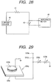
In Fig. 26, another configuration example of the
circuit wherein the semiconductor laser gyro is driven
by a constant current and a change in the anode
potential of the semiconductor laser gyro 40 is read
out so as to detect the rotation. The same reference
numerals are attached to the same components with Fig.
24.
The anode of the semiconductor laser gyro 40 is
connected to the output terminal of the operational
amplifier 55 via a protective resistor 52 and the
cathode of the semiconductor laser gyro 40 is connected
to the inversion input terminal of the operational
amplifier 55. Also, a resistor 53 is connected between
the inversion input terminal and the reference
potential of the operational amplifier 55.
Here, when a controlled potential (V in) is given
to the non-inversion input terminal of the operational
amplifier 55 from a microcomputer 54 and the like, the
current derived from the above potential and a resistor
53 becomes the constant current flowed to the
semiconductor laser gyro 40 for driving. The anode of
the semiconductor laser gyro 40 is connected to the
operational amplifier 45. The operational amplifier 45
outputs a signal Vout. Since this signal has the beat
frequency proportional to the angular speed, it is
converted into a voltage by the publicly known
frequency-voltage conversion circuit 50 (a F-V
conversion circuit) and the like so that a rotation is
detected by a rotation detector 51.
Note that, in Fig. 27, the example of the
frequency-voltage conversion circuit (a F-V conversion
circuit) is shown. This circuit is configured by
transistor Tr1, diodes D1 and D2, condensers C1 and C2
and resistances R0 and R1. EC denotes a bias voltage.
An output voltage VC2 is given by the following Equation
(19):
VC2 = E1C1R0f 1+11-exp(-1/(R0C2f))
Here, E1 denotes a peak to peak value of an input
voltage and f denotes a beat frequency. By designing a
circuit parameter such that it becomes C2>>C1, ROC2f<1,
the following Equation (20) is given:
VC2 ≃ E1C1R0f/2
so that the voltage output proportional to the beat
frequency can be obtained.
Also, regardless of the kind of the current
source, a change in the impedance of the semiconductor
laser can be also directly measured by an impedance
meter 49. Reference numeral 44 denotes the current
source. In this case, different from the case where
the terminal voltage is measured, the effect of a noise
of the driving current source becomes small. This
example is shown in Fig. 28. Numeral 40 denotes a
semiconductor laser gyro, and numeral 41 denotes a
resistance.
[Embodiment 3]
Figs. 14A to 14D are drawings most properly
showing the characteristics of the present invention.
Fig. 14A is a top view of the semiconductor laser gyro
of the present invention. Fig. 14B is a sectional view
cut along 14B-14B line of Fig. 14A.
In the same drawing, reference numerals 1, 2, 3
and 4 denote anodes, reference numerals 11, 12, 13 and
14 cathodes, reference numeral 121 a semiconductor
substrate, reference numeral 22 a buffer layer,
reference numeral 23 an optical guiding layer,
reference numeral 24 an active layer, reference numeral
25 an optical guiding layer, reference numeral 26 a
cladding layer and reference numeral 27 a cap layer.
Also, Fig. 15 to Fig. 23 are sectional views explaining
the manufacturing process of the semiconductor laser
gyro of the present invention. In the same drawings,
reference numeral 28 denotes an anode material,
reference numeral 29 a cathode material and reference
numerals 31, 32 photoresists. Note that Fig. 14C is a
sectional view cut along 14C-14C line in Fig. 14A and
Fig. 14D is a sectional view cut along 14D-14D line in
Fig. 14A.
Hereinafter, with reference to Fig. 15 to Fig. 23,
the manufacturing process of the semiconductor laser
gyro of the present invention will be described.
First, as shown in Fig. 15, by using metal organic
vapor phase epitaxial growth techniques, an InP buffer
layer 22 (a thickness of 0.05 µm), an undoped InGaAsP
optical guiding layer 23 having 1.3 µm composition (a
thickness of 0.15 µm), an undoped InGaAsP active layer
24 having 1.55 µm composition (a thickness of 0.1 µm),
an undoped InGaAsP optical guiding layer 25 having 1.3
pm composition (a thickness of 0.15 µm), a p-InP
cladding layer 26 (a thickness of 2 µm) and a p-InGaAsP
cap layer 27 having 1.4 µm composition (a thickness of
0.3 µm) are grown on a semi-insulating-InP substrate
121 (a thickness of 350 µm). After the grain growth
thereof, as shown in Fig. 16, a Cr/Au as an anode
material 28 is formed by vapor deposition on the p-InGaAsP
cap layer 27. Then, by using a spin coater, an
AZ-1350 (manufactured by Hoechst) is coated as a
photoresist 31 on the anode material 28 in such a
manner that the coating thickness thereof becomes 1 µm.
After a heat treatment is conducted as a pre-baking at
a temperature of 80 degrees for 30 minutes, a wafer is
exposed by masking. The photoresist 31 after
development and rinse has a slightly tapered shape as
shown in Fig. 17. Also, the width of the stripe
thereof is 5 µm and the length of one cycle of the
optical waveguide is 600 µm. Thereafter, the wafer is
guided to a reactive ion etching system and, as shown
in Fig. 18, the Cr/Au of the anode material 28 is dry-etched
with the photoresist 31 as an etching mask. The
gas employed for the etching is Ar for Au and CF4 for
Cr. Next, by using a chlorine gas, the semiconductor
layer is etched so that the height of an optical
waveguide becomes 3.2 µm. This aspect is shown in Fig.
19 and, as shown in Fig. 20, the photoresist 31 is
removed. Subsequently, the photoresist undergoes the
patterning and the Cr/Au of a corner portion and the
cap layer are etched and the intervals of the anodes
are electrically insulated. The separation resistance
between the anodes is 1 kΩ. Thereafter, the anode 28
is annealed in a hydrogen atmosphere and an ohmic
contact is realized. Next, in order to form the
cathode by a lift off, by using a spin coater, a
photoresist 32 is coated so as to cover the whole
surface of the wafer. The photoresist 32 is RD-2000N
(manufactured by Hitachi Kasei) and has a thickness of
1 µm. After a pre-baking is conducted at a temperature
of 90 degrees for 30 minutes, the wafer is exposed by
masking. The photoresist 32 after development and
rinse has a reversed tapered shape suitable for the
lift off as shown in Fig. 21. Subsequently, as shown
in Fig. 22, AuGe/Ni/Au is deposited as a cathode
material 29 on the n-InP substrate 121. Thereafter, by
rinsing this wafer in an organic solvent by ultrasonic
wave, a cathode 29 is selectively formed as shown in
Fig. 23. In order that the current is flowed only
across each pair of the anode/the cathode, the
intervals of the cathodes are also insulated by using
ion injection and the like. Also, the intervals of the
cathodes may be separated through patterning. Finally,
the cathodes are annealed in the hydrogen atmosphere
with ohmic contact realized.
Next, by using Figs. 14A to 14D, the operation of
the semiconductor laser gyro will be described. In
this embodiment, the anodes and the cathodes are
segmented into four pieces, and one piece each of the
anode and one piece each of the cathode are used as one
pair. By combining the anode 1 with the cathode 11,
the anode 2 with the cathode 12, the anode 3 with the
cathode 13 and the anode 4 with the cathode 14
respectively, the current is injected to the intervals
of each pair. Since the anode electrode and the
cathode electrode are independent respectively, the
current, for example, does not flow across the anode 2
and the cathode 11. In Fig. 14A, the anodes 1, 2 are
depicted as if they touch with each other, but actually
they are separated as shown in Fig. 1C. At this time,
in Fig. 14A, the electron moves counterclockwise.
Since the semiconductor and the air are different
in respect of the refractive index, a reflection is
caused on the interface. Assuming that the refractive
index n of the semiconductor is n = 3.5, a total
reflection is caused by not less than 16.6 degrees of
the angle made by a normal line and a laser beam
against the interface. Since the mode whose field is
totally reflected, has low oscillating threshold in
contrast to another mode by a degree where no mirror
loss is found, an oscillation begins at low injected
current. Moreover, because a gain is concentrated into
this oscillating mode, other oscillation modes are
suppressed. In the semiconductor laser gyro of Figs.
14A to 14D, the incident angle of the laser beam at
four corners is 45 degrees and satisfies the condition
of the total reflection. As a result, the oscillating
threshold at a room temperature is only 3 mA. A
driving current is 4.5 mA and, when this laser is in a
stationary state, the oscillating wavelength λo in a
vacuum is 1.55 µm.
Next, the beat frequency in a stationary state is
considered. Since a diffusion length Ln of the electron
is Ln = 2 µm and a recombination life τn = 1 x 10⁻⁸s, the
speed of the electron v is given by the following
Equation (21):
v=Ln τn =2×10² m/s
Also, the oscillating wavelength in a vacuum λo = 1.55
µm and the refractive index n of the semiconductor is n
= 3.5. At this time, the beat frequency Δf in a
stationary state is given by the following Equation
(22):
Δf = 9.0 × 10⁸ Hz = 900 MHz
Moreover, when the semiconductor laser gyro of
Fig. 1A to Fig. 1C is rotated counterclockwise at the
speed of 30 degrees per second with a measure of a
camera shake and the vibration of an automobile, the
oscillating frequency f2 of the laser beam clockwise is
increased by 88.7 Hz. On the other hand, the
oscillating frequency f1 of the laser beam
counterclockwise is decreased by 88.7 Hz. As a result,
as shown in the Equation (13), in contrast to the
semiconductor in a stationary state, the beat frequency
is increased by 177.4 Hz. On the other hand, when the
semiconductor laser gyro is given a rotation clockwise
at the speed of 30 degrees per second, as shown in the
Equation (14), in contrast to the semiconductor in a
stationary state, the beat frequency is decreased by
177.4 Hz. Thus, by increase and decrease in the beat
frequency, the direction of a rotation can be detected.
Moreover, since the absolute value of the amount of
change in the beat frequency corresponds to the speed
of a rotation, the speed of a rotation can be also
measured. That is, by the present invention, the speed
of a rotation and the direction of a rotation can be
detected at the same time. Note that this beat
frequency is observed from a change in the terminal
voltage if a constant current is flowed to the
semiconductor laser. Note that Fig. 14A shows the case
where a pair of the anode and the cathode is used in
four pairs. However, it is preferable that the current
area where the current flows in the same direction with
the laser beam is available in a part of the electrode
area.
Here, the material of the InGaAsP system was used
as the material of the semiconductor. However, the
material system such as GaAs system, ZnSe system, InGaN
system, Al-GaN system and the like may be also used.
Also, concerning the optical waveguide, the shape
surrounding the optical path may be not only square as
shown in Figs. 1A to 1C, but whichever shape may be
used such as hexagon, triangle or circle and the like.
Moreover, the number of anodes and cathodes is not
limited to four as shown in the present embodiment, but
any number may be used if plural.
Note that, concerning the method for detecting a
rotation from a change in the voltage (a change in the
frequency of the voltage) of the semiconductor laser
gyro, the method described as above can be used.
As described above, according to the present
invention, the direction of a rotation can be detected
even if a dither is not driven.
A ring laser gyro wherein a first and a second
laser beam propagate with propagating directions
different with each other comprises electrode areas on
an optical waveguide configuring the ring laser and
controls an current injected or a voltage applied to
the electrode areas, wherein the oscillating
frequencies of the first and second laser beams are
different from each other, thereby causing an increase
and a decrease in the beat frequency enabling to detect
the direction and the speed of a rotation at the same
time. With regards to a method for detecting a
rotation, the anode of the laser gyro is connected to
an operational amplifier. Since the signal outputted
from the operational amplifier has a frequency
corresponding to the angular speed, it is converted
into the voltage by a frequency-voltage conversion
circuit so as to detect a rotation. This same method
can be used for other types of gyros such as a
semiconductor laser gyro, a gas lager gyro and the
like.