EP1099931A2 - Ring laser gyro - Google Patents
Ring laser gyro Download PDFInfo
- Publication number
- EP1099931A2 EP1099931A2 EP00124454A EP00124454A EP1099931A2 EP 1099931 A2 EP1099931 A2 EP 1099931A2 EP 00124454 A EP00124454 A EP 00124454A EP 00124454 A EP00124454 A EP 00124454A EP 1099931 A2 EP1099931 A2 EP 1099931A2
- Authority
- EP
- European Patent Office
- Prior art keywords
- laser gyro
- semiconductor laser
- current
- gyro
- rotation
- Prior art date
- Legal status (The legal status is an assumption and is not a legal conclusion. Google has not performed a legal analysis and makes no representation as to the accuracy of the status listed.)
- Withdrawn
Links
- 230000003287 optical effect Effects 0.000 claims abstract description 37
- 230000001902 propagating effect Effects 0.000 claims abstract description 37
- 230000000644 propagated effect Effects 0.000 claims description 3
- 239000004065 semiconductor Substances 0.000 abstract description 105
- 230000035559 beat frequency Effects 0.000 abstract description 41
- 238000000034 method Methods 0.000 abstract description 22
- 238000006243 chemical reaction Methods 0.000 abstract description 10
- 239000007789 gas Substances 0.000 description 20
- 238000004519 manufacturing process Methods 0.000 description 20
- 229920002120 photoresistant polymer Polymers 0.000 description 15
- 230000000694 effects Effects 0.000 description 12
- 239000010405 anode material Substances 0.000 description 8
- 239000000203 mixture Substances 0.000 description 8
- 230000003247 decreasing effect Effects 0.000 description 7
- 239000000758 substrate Substances 0.000 description 7
- 239000000463 material Substances 0.000 description 6
- 230000010355 oscillation Effects 0.000 description 5
- UFHFLCQGNIYNRP-UHFFFAOYSA-N Hydrogen Chemical compound [H][H] UFHFLCQGNIYNRP-UHFFFAOYSA-N 0.000 description 4
- 238000005253 cladding Methods 0.000 description 4
- 238000005530 etching Methods 0.000 description 4
- 239000001257 hydrogen Substances 0.000 description 4
- 229910052739 hydrogen Inorganic materials 0.000 description 4
- 230000008878 coupling Effects 0.000 description 3
- 238000010168 coupling process Methods 0.000 description 3
- 238000005859 coupling reaction Methods 0.000 description 3
- 238000002347 injection Methods 0.000 description 3
- 239000007924 injection Substances 0.000 description 3
- 230000000873 masking effect Effects 0.000 description 3
- 238000000059 patterning Methods 0.000 description 3
- 230000001681 protective effect Effects 0.000 description 3
- KZBUYRJDOAKODT-UHFFFAOYSA-N Chlorine Chemical compound ClCl KZBUYRJDOAKODT-UHFFFAOYSA-N 0.000 description 2
- 229910001218 Gallium arsenide Inorganic materials 0.000 description 2
- 229910003327 LiNbO3 Inorganic materials 0.000 description 2
- 239000010406 cathode material Substances 0.000 description 2
- 239000011248 coating agent Substances 0.000 description 2
- 238000000576 coating method Methods 0.000 description 2
- 238000001514 detection method Methods 0.000 description 2
- 230000020169 heat generation Effects 0.000 description 2
- 238000010438 heat treatment Methods 0.000 description 2
- 239000001307 helium Substances 0.000 description 2
- 229910052734 helium Inorganic materials 0.000 description 2
- SWQJXJOGLNCZEY-UHFFFAOYSA-N helium atom Chemical compound [He] SWQJXJOGLNCZEY-UHFFFAOYSA-N 0.000 description 2
- 239000002184 metal Substances 0.000 description 2
- 229910052754 neon Inorganic materials 0.000 description 2
- GKAOGPIIYCISHV-UHFFFAOYSA-N neon atom Chemical compound [Ne] GKAOGPIIYCISHV-UHFFFAOYSA-N 0.000 description 2
- 238000001020 plasma etching Methods 0.000 description 2
- 230000005701 quantum confined stark effect Effects 0.000 description 2
- SBIBMFFZSBJNJF-UHFFFAOYSA-N selenium;zinc Chemical compound [Se]=[Zn] SBIBMFFZSBJNJF-UHFFFAOYSA-N 0.000 description 2
- 238000000926 separation method Methods 0.000 description 2
- 238000007740 vapor deposition Methods 0.000 description 2
- 239000012808 vapor phase Substances 0.000 description 2
- 230000000903 blocking effect Effects 0.000 description 1
- 239000003990 capacitor Substances 0.000 description 1
- 230000015556 catabolic process Effects 0.000 description 1
- 239000013078 crystal Substances 0.000 description 1
- 230000006866 deterioration Effects 0.000 description 1
- 238000009792 diffusion process Methods 0.000 description 1
- 230000005684 electric field Effects 0.000 description 1
- 238000005516 engineering process Methods 0.000 description 1
- 125000005842 heteroatom Chemical group 0.000 description 1
- 239000013307 optical fiber Substances 0.000 description 1
- 230000005693 optoelectronics Effects 0.000 description 1
- 239000003960 organic solvent Substances 0.000 description 1
- 230000010287 polarization Effects 0.000 description 1
- 230000006798 recombination Effects 0.000 description 1
- 238000005215 recombination Methods 0.000 description 1
Images







Classifications
-
- G—PHYSICS
- G01—MEASURING; TESTING
- G01C—MEASURING DISTANCES, LEVELS OR BEARINGS; SURVEYING; NAVIGATION; GYROSCOPIC INSTRUMENTS; PHOTOGRAMMETRY OR VIDEOGRAMMETRY
- G01C1/00—Measuring angles
-
- G—PHYSICS
- G01—MEASURING; TESTING
- G01C—MEASURING DISTANCES, LEVELS OR BEARINGS; SURVEYING; NAVIGATION; GYROSCOPIC INSTRUMENTS; PHOTOGRAMMETRY OR VIDEOGRAMMETRY
- G01C19/00—Gyroscopes; Turn-sensitive devices using vibrating masses; Turn-sensitive devices without moving masses; Measuring angular rate using gyroscopic effects
- G01C19/58—Turn-sensitive devices without moving masses
- G01C19/64—Gyrometers using the Sagnac effect, i.e. rotation-induced shifts between counter-rotating electromagnetic beams
- G01C19/66—Ring laser gyrometers
Definitions
- the present invention relates to a laser gyro, a semiconductor laser gyro, a method for driving the laser gyro and the method for driving the semiconductor laser gyro and, in particular, to a laser gyro of ring resonator type.
- the optical gyros include laser gyros, optical fiber gyros, passive resonator gyros and the like. Among them, a laser gyro employing a gas laser was most early undertaken to develop and already put to practical use in the art of aircrafts and the like.
- a semiconductor laser element 5792 has electrodes 5790, 5791 above and below it.
- Reference numeral 5793 denotes a direct current blocking capacitor, reference numeral 5794 an output terminal, and reference numeral 5795 a resistor. It is disclosed that, as shown in Fig. 29, the semiconductor laser element as a laser element for the ring laser device is connected to a driving power source 5796, and a frequency difference (a beat frequency) between light beams clockwise and counterclockwise generated when a certain angular speed is given to the above device is detected as a difference between the terminal voltages of the laser element.
- a frequency difference a beat frequency
- the conventional laser gyro cannot detect a rotation direction. This is because the beat frequencies detected from the terminal voltage has the same value whether the rotating direction of the semiconductor laser element is clockwise or counterclockwise. For this reason, dithering was effected and, from the correlation between the direction and signal of the dither, the rotating direction was determined.
- the ring laser gyro according to the present invention is a ring laser gyro in which first and second laser beams propagate in opposite directions from each other, characterized in that plural electrode areas are provided on an optical waveguide comprised in the ring laser, and current injected or voltage applied to the electrode areas is controlled, so that the oscillating frequencies of the first and second laser beams become different from each other at a time when the ring laser gyro is in a stationary state.
- the above control is such that current is injected to the plural electrodes so that a space in which the refractive index of the optical waveguide is modulated moves in the same direction as the propagating direction of the first or second laser beam as time goes on.
- the above control is such that injected current is propagated in the same direction as the propagating direction of the first or second laser beam.
- a method for driving the ring laser gyro according to the present invention is characterized in that a space in which the refractive index of an optical waveguide is modulated moves in one propagating direction as time goes on.
- the method for driving the ring laser gyro is a method for driving ring laser gyro having plural electrodes, characterized in that voltage applied or current injected to the plural electrodes is modulated with a time difference set among the electrodes so that a sequence of modulations is in a propagating direction.
- the method for driving the ring laser gyro according to the present invention is a method for driving the semiconductor laser gyro in which by flowing the current to generate laser oscillation light is propagated in one propagating direction or in the propagating direction opposite to the one propagating direction, characterized in that the flowing direction of the current is limited to the one propagating direction.
- Fig. 9A shows a top view of the semiconductor laser gyro and Fig. 9B shows a timing chart for the current injected to each electrode.
- reference numerals 1, 2, 3 and 4 denote anodes and each anode is electrically separated.
- the current is injected to anodes 1, 2 and 3 with a time difference set up across them.
- the shape of the anodes 1 to 4 is not limited to the shape as shown in the drawing, but may be the shape in which the current can be injected similarly to a timing chart as shown in Fig. 9B.
- Equation (2) Equation (2) is given from the special theory of relativity:
- m represents the number of electrodes for modulating the current.
- m 3 because the electrodes 1, 2 and 3 are employed.
- a direct current is flowed to the two remaining electrodes where no current is modulated.
- L denotes a whole length of the resonator, ⁇ 0 an oscillating wave length in a vacuum when the equivalent refractive index of an optical resonator is n 0 .
- a constant current for example, 4 mA
- the current may not be flowed.
- a beat light having the beat frequency ⁇ f n is generated inside a semiconductor laser and a total light intensity inside the semiconductor laser fluctuates at a beat frequency ⁇ f.
- a carrier concentration in an active layer fluctuates at the beat frequency and, when a constant current is flowed into the semiconductor laser, a terminal voltage changes at the beat frequency.
- a beat signal is observed from the electrical terminal of the element.
- the semiconductor laser gyro according to the present invention is characterized in that the injected current is flowed to one propagating direction, if the flowing direction of the current is one propagating direction, the propagating direction of the carrier is also one direction.
- the carrier in case of the semiconductor laser, while the carrier is confined by a double hetero structure in respect of the growth direction of a semiconductor layer, it can freely move about inside the surface of the semiconductor layer.
- the present invention utilizes the movement of this carrier (mainly the electron) inside the surface of the semiconductor layer and, for this reason, the current injected to the semiconductor laser may have a driving means for propagating in one direction at least in a part of area.
- the propagating direction of the electron is narrowed down to one direction.
- the resonant frequency where a gain becomes the highest varies according to the light propagating clockwise and the light propagating counterclockwise.
- the speed v thereof is represented by v > 0.
- Equations (8) and (9) the resonant frequency f 1 of the light counterclockwise and the resonant frequency f 2 of the light clockwise are given by the following Equations (8) and (9):
- f 0 denotes the resonant frequency of the light when there is no Doppler effect available
- c denotes the light speed in a vacuum
- n denotes the refractive index of the semiconductor.
- the coupling between two counterpropagating oscillating modes i.e. the coupling between two oscillating modes propagating in opposite directions from each other becomes a weak coupling.
- these two modes will oscillate independently from each other. That is, inside the ring resonator, there coexist two counterpropagating oscillating modes where the oscillating frequencies are shifted due to Doppler effect.
- the carrier concentration in an active layer fluctuates at the beat frequency and, if a constant current is flowed to the semiconductor laser, the terminal voltage fluctuates at the beat frequency.
- a beat signal is observed from the electrical terminal of the element even when this element is in a stationary state.
- the semiconductor laser is preferably in the shape of a ring.
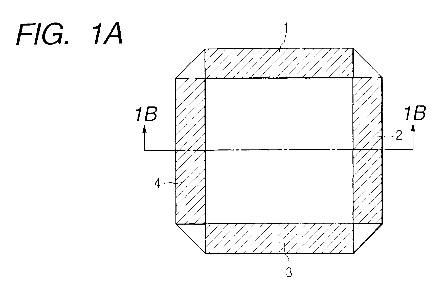
- Figs. 1A to 1C are drawings most properly showing the characteristic of the present invention
- Fig. 1A is a top view of a semiconductor laser gyro of the present invention
- Fig. 1B is a sectional view cut along 1B-1B line in Fig. 1A.
- reference numerals 1, 2, 3 and 4 denote anodes, reference numeral 11 a cathode, reference numeral 21 a semiconductor substrate, reference numeral 22 a buffer layer, reference numeral 23 an optical guiding layer, reference numeral 24 an active layer, reference numeral 25 an optical guiding layer, reference numeral 26 a cladding layer and reference numeral 27 a cap layer.
- anodes look like partially touching with each other, but actually they are separated from each other as shown in Fig. 1C.
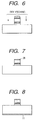
- Fig. 2 to Fig. 8 are sectional views explaining the manufacturing process of the semiconductor laser gyro of the present invention. Note that the same reference numerals are attached to the same components with Figs. 1A to 1C.
- reference numeral 28 denotes an anode material and reference numeral 31 a photoresist.
- an InP buffer layer 22 (a thickness of 0.05 ⁇ m), an undoped InGaAsP optical guiding layer 23 having 1.3 ⁇ m composition (a thickness of 0.15 ⁇ m), an undoped InGaAsP active layer 24 having 1.55 ⁇ m composition (a thickness of 0.1 ⁇ m), an undoped InGaAsP optical guiding layer 25 having 1.3 ⁇ m composition (a thickness of 0.15 ⁇ m), a p-InP cladding layer 26 (a thickness of 2 ⁇ m) and a p-InGaAsP cap layer 27 having 1.4 ⁇ m composition (a thickness of 0.3 ⁇ m)are grown on an n-InP substrate 21 (a thickness of 350 ⁇ m).
- a Cr/Au as an anode material 28 is formed by vapor deposition on the p-InGaAsP cap layer 27. Then, by using a spin coater, an AZ-1350 (manufactured by Hoechst) is coated as a photoresist 31 on the anode material 28 in such a manner that the coating thickness thereof becomes 1 ⁇ m. After a heat treatment is conducted as a pre-baking at a temperature of 80 degrees for 30 minutes, a wafer is exposed by masking. The photoresist 31 after development and rinse has a slightly tapered shape as shown in Fig. 4.
- the width of the stripe thereof is 5 ⁇ m and the length of one side of the electrode is 100 pm.
- the wafer is guided to a reactive ion etching system and, as shown in Fig. 5, the Cr/Au of the anode material 28 is dry-etched with the photoresist 31 as an etching mask.
- the gas employed for the etching is Ar for Au and CF 4 for Cr.
- the semiconductor layer is etched so that the height of an optical waveguide becomes 3.2 ⁇ m. This aspect is shown in Fig. 6 and, as shown in Fig. 7, the photoresist 31 is removed.
- the photoresist undergoes the patterning once again and the Cr/Au of a corner portion and the cap layer are etched and the intervals of the anodes are electrically insulated.
- the separation resistance between the anodes is 1 K ⁇ .
- the anode 28 is annealed in a hydrogen atmosphere and an ohmic contact is realized.
- AuGe/Ni/Au as the cathode 11 is vapordeposited on the n-InP substrate 21, which is finally annealed in the hydrogen atmosphere with ohmic contact realized.
- Figs. 9A and 9B the operation of the semiconductor laser gyro will be described.
- the anodes are segmented into four pieces, and one piece of the anode and one piece of the cathode are used as one pair.
- the current is flowed to the anodes 1, 2 and 3 with a timing as shown in Fig. 9B.
- a constant current 4 mA is injected to the electrode 4.
- the incident angle of the laser beam at four corners is 45 degrees and satisfies the condition of the total reflection.
- the oscillating threshold in a room temperature is only 2 mA.
- a driving current is 3 mA and, when this laser is in a stationary state and a uniform current is injected to the four electrodes, the oscillating wavelength ⁇ o in a vacuum is 1.55 ⁇ m.
- the beat frequency in a stationary state is considered.
- the oscillating frequency f 2 of the laser beam clockwise is increased by 59.1 Hz.
- the oscillating frequency f 1 of the laser beam counterclockwise is decreased by 59.1 Hz.
- the beat frequency is increased by 118.2 Hz.
- the beat frequency is decreased by 118.2 Hz.
- the absolute value of the amount of change in the beat frequency corresponds biuniquely to the speed of a rotation
- the speed of a rotation can be also measured. That is, by the present invention, the speed of a rotation and the direction of a rotation can be detected at the same time. Note that this beat frequency is observed from a change in the terminal voltage if a constant current is injected to the semiconductor laser.
- the material of the InGaAsP system was used as the material of the semiconductor.
- the material system such as GaAs system, ZnSe system, InGaN system, Al-GaN system and the like may be also used.
- the shape surrounding the optical path may be not only square, but whichever shape may be used such as hexagon, triangle or circle and the like as shown in Fig. 9A.
- the number of anodes and cathodes is not limited to four as shown in the present embodiment, but any number may be used if plural.
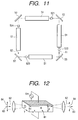
- Fig. 11 is a typical plan view showing one sample of an optical gyro provided with a resonator type gas laser in which light propagates circularly according to the present invention and the case where the propagating path of the laser beam is square.
- reference numeral 51 denotes a discharge tube
- reference numeral 53 a mirror
- reference numeral 61 a laser beam clockwise
- reference numeral 62 a counterclockwise laser beam.
- the discharge begins and the state is such that the current flows.
- the distances between the mirrors 53 are set to be 10 cm.
- the oscillating frequencies of the laser beams clockwise and counterclockwise are quite identical which are 4.73 ⁇ 10 14 Hz and have an oscillating wavelength ⁇ of 632.8 nm.
- the refractive index modulating elements 521, 522, 523 and 524 are Ti diffused LiNbO 3 refractive index modulating elements and change the refractive index by using electro-optical effect.
- Fig. 12 The typical perspective view of this element is shown in Fig. 12.
- numeral 81 denotes a LiNbO 3 crystal.
- the refractive index n P for the propagating direction 83 of the laser beam 82 is 2.286.
- Arrows 84 lying at right angles to the propagating direction 83 show directions of polarization of the light, i.e. directions in which the electric field oscillates.
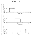
- the voltage is applied to the refractive index modulating elements 521, 522 and 523 with a timing as shown in Fig. 13. At this time, the voltage is all constant and 5V.
- the beat frequency in a stationary state is considered.
- v is given by the following Equation (17):
- the oscillating frequency f 2 of the laser beam clockwise is decreased by 41.4 kHz.
- the oscillating frequency f 1 of the laser beam counterclockwise is decreased by 41.4 kHz.
- the direction of a rotation can be detected.
- the absolute value of the amount of change in the beat frequency corresponds biuniquely to the speed of a rotation
- the speed of a rotation can be measured. That is, by the present invention, a speed of a rotation and the direction of a rotation can be detected at the same time. Note that this beat frequency is observed from a change in the terminal voltage of the discharge tube if a constant current is flowed to the discharge tube configuring the gas laser.
- any gas may be used if it makes a laser oscillation.
- the shape of the resonator is not limited to square, but whichever shape may be used such as hexagon, triangle and the like.
- the refractive index modulating element utilizing not only electro-optic effect but also accousto-optic effect and heat effect may be used.
- a method for detecting a rotation from a change in the voltage (a change in the frequency of the voltage) of the laser gyro such as the semiconductor laser gyro, the gas laser gyro and the like will be described. While an example of the semiconductor laser gyro is adapted here, the same method can be used also for the gas laser gyro.
- the method for detecting a direction from a change in the voltage (a change in the frequency of the voltage) of the semiconductor laser gyro 40 is shown.
- reference numeral 40 denotes the semiconductor laser gyro
- reference numeral 41 an electrical resistance
- reference numeral 42 a constant current source
- reference numeral 46 a voltage detection circuit.
- a protective circuit By disposing a protective circuit on the detection terminal of the semiconductor laser gyro, the deterioration or the breakdown of the semiconductor laser gyro can be prevented.
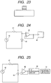
- a voltage follower 45 is connected as the protective circuit as shown in Fig. 24.
- the anode of the semiconductor laser gyro 40 is connected to an operational amplifier 45 for buffer. Since the signal outputted from the operational amplifier 45 has a frequency corresponding to the angular speed, it is converted into the voltage by a known frequency-voltage conversion circuit 50 (a F-V conversion circuit) so as to detect the rotation through a rotation detector 51. Of course, if the desired characteristics are obtained, the operational amplifier 45 (a voltage follower) may be omitted.
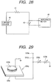
- FIG. 26 another configuration example of the circuit wherein the semiconductor laser gyro is driven by a constant current and a change in the anode potential of the semiconductor laser gyro 40 is read out so as to detect the rotation.
- the same reference numerals are attached to the same components with Fig. 24.
- the anode of the semiconductor laser gyro 40 is connected to the output terminal of the operational amplifier 55 via a protective resistor 52 and the cathode of the semiconductor laser gyro 40 is connected to the inversion input terminal of the operational amplifier 55. Also, a resistor 53 is connected between the inversion input terminal and the reference potential of the operational amplifier 55.
- Fig. 27 the example of the frequency-voltage conversion circuit (a F-V conversion circuit) is shown.
- This circuit is configured by transistor Tr 1 , diodes D 1 and D 2 , condensers C 1 and C 2 and resistances R 0 and R 1 .
- E C denotes a bias voltage.
- E 1 denotes a peak to peak value of an input voltage
- f denotes a beat frequency.
- Equation (20) V C2 ⁇ E 1 C 1 R 0 f/2 so that the voltage output proportional to the beat frequency can be obtained.
- a change in the impedance of the semiconductor laser can be also directly measured by an impedance meter 49.
- Reference numeral 44 denotes the current source. In this case, different from the case where the terminal voltage is measured, the effect of a noise of the driving current source becomes small. This example is shown in Fig. 28.
- Numeral 40 denotes a semiconductor laser gyro
- numeral 41 denotes a resistance.
- Figs. 14A to 14D are drawings most properly showing the characteristics of the present invention.
- Fig. 14A is a top view of the semiconductor laser gyro of the present invention.
- Fig. 14B is a sectional view cut along 14B-14B line of Fig. 14A.
- reference numerals 1, 2, 3 and 4 denote anodes, reference numerals 11, 12, 13 and 14 cathodes, reference numeral 121 a semiconductor substrate, reference numeral 22 a buffer layer, reference numeral 23 an optical guiding layer, reference numeral 24 an active layer, reference numeral 25 an optical guiding layer, reference numeral 26 a cladding layer and reference numeral 27 a cap layer.
- Fig. 15 to Fig. 23 are sectional views explaining the manufacturing process of the semiconductor laser gyro of the present invention.
- reference numeral 28 denotes an anode material
- reference numeral 29 a cathode material
- reference numerals 31, 32 photoresists denotes an anode material
- Fig. 14C is a sectional view cut along 14C-14C line in Fig. 14A
- Fig. 14D is a sectional view cut along 14D-14D line in Fig. 14A.
- an InP buffer layer 22 (a thickness of 0.05 ⁇ m), an undoped InGaAsP optical guiding layer 23 having 1.3 ⁇ m composition (a thickness of 0.15 ⁇ m), an undoped InGaAsP active layer 24 having 1.55 ⁇ m composition (a thickness of 0.1 ⁇ m), an undoped InGaAsP optical guiding layer 25 having 1.3 pm composition (a thickness of 0.15 ⁇ m), a p-InP cladding layer 26 (a thickness of 2 ⁇ m) and a p-InGaAsP cap layer 27 having 1.4 ⁇ m composition (a thickness of 0.3 ⁇ m) are grown on a semi-insulating-InP substrate 121 (a thickness of 350 ⁇ m).
- a Cr/Au as an anode material 28 is formed by vapor deposition on the p-InGaAsP cap layer 27. Then, by using a spin coater, an AZ-1350 (manufactured by Hoechst) is coated as a photoresist 31 on the anode material 28 in such a manner that the coating thickness thereof becomes 1 ⁇ m. After a heat treatment is conducted as a pre-baking at a temperature of 80 degrees for 30 minutes, a wafer is exposed by masking. The photoresist 31 after development and rinse has a slightly tapered shape as shown in Fig. 17.
- the width of the stripe thereof is 5 ⁇ m and the length of one cycle of the optical waveguide is 600 ⁇ m.
- the wafer is guided to a reactive ion etching system and, as shown in Fig. 18, the Cr/Au of the anode material 28 is dry-etched with the photoresist 31 as an etching mask.
- the gas employed for the etching is Ar for Au and CF 4 for Cr.
- the semiconductor layer is etched so that the height of an optical waveguide becomes 3.2 ⁇ m. This aspect is shown in Fig. 19 and, as shown in Fig. 20, the photoresist 31 is removed.
- the photoresist undergoes the patterning and the Cr/Au of a corner portion and the cap layer are etched and the intervals of the anodes are electrically insulated.
- the separation resistance between the anodes is 1 k ⁇ .
- the anode 28 is annealed in a hydrogen atmosphere and an ohmic contact is realized.
- a photoresist 32 is coated so as to cover the whole surface of the wafer.
- the photoresist 32 is RD-2000N (manufactured by Hitachi Kasei) and has a thickness of 1 ⁇ m.
- the wafer After a pre-baking is conducted at a temperature of 90 degrees for 30 minutes, the wafer is exposed by masking.
- the photoresist 32 after development and rinse has a reversed tapered shape suitable for the lift off as shown in Fig. 21.
- AuGe/Ni/Au is deposited as a cathode material 29 on the n-InP substrate 121.
- a cathode 29 is selectively formed as shown in Fig. 23.
- the intervals of the cathodes are also insulated by using ion injection and the like. Also, the intervals of the cathodes may be separated through patterning. Finally, the cathodes are annealed in the hydrogen atmosphere with ohmic contact realized.
- the anodes and the cathodes are segmented into four pieces, and one piece each of the anode and one piece each of the cathode are used as one pair.
- the current is injected to the intervals of each pair. Since the anode electrode and the cathode electrode are independent respectively, the current, for example, does not flow across the anode 2 and the cathode 11.
- the anodes 1, 2 are depicted as if they touch with each other, but actually they are separated as shown in Fig. 1C. At this time, in Fig. 14A, the electron moves counterclockwise.
- the oscillating frequency f 2 of the laser beam clockwise is increased by 88.7 Hz.
- the oscillating frequency f 1 of the laser beam counterclockwise is decreased by 88.7 Hz.
- the beat frequency is increased by 177.4 Hz.
- the material of the InGaAsP system was used as the material of the semiconductor.
- the material system such as GaAs system, ZnSe system, InGaN system, Al-GaN system and the like may be also used.
- the shape surrounding the optical path may be not only square as shown in Figs. 1A to 1C, but whichever shape may be used such as hexagon, triangle or circle and the like.
- the number of anodes and cathodes is not limited to four as shown in the present embodiment, but any number may be used if plural.
- the direction of a rotation can be detected even if a dither is not driven.
- a ring laser gyro wherein a first and a second laser beam propagate with propagating directions different with each other comprises electrode areas on an optical waveguide configuring the ring laser and controls an current injected or a voltage applied to the electrode areas, wherein the oscillating frequencies of the first and second laser beams are different from each other, thereby causing an increase and a decrease in the beat frequency enabling to detect the direction and the speed of a rotation at the same time.
- the anode of the laser gyro is connected to an operational amplifier. Since the signal outputted from the operational amplifier has a frequency corresponding to the angular speed, it is converted into the voltage by a frequency-voltage conversion circuit so as to detect a rotation.
- This same method can be used for other types of gyros such as a semiconductor laser gyro, a gas lager gyro and the like.
Landscapes
- Physics & Mathematics (AREA)
- Engineering & Computer Science (AREA)
- General Physics & Mathematics (AREA)
- Radar, Positioning & Navigation (AREA)
- Remote Sensing (AREA)
- Optics & Photonics (AREA)
- Electromagnetism (AREA)
- Power Engineering (AREA)
- Gyroscopes (AREA)
- Semiconductor Lasers (AREA)
- Lasers (AREA)
Abstract

Description


Claims (4)
- A ring laser gyro in which first and second laser beams propagate in opposite directions from each other, characterized in that electrode areas are provided on an optical waveguide comprised in the ring laser, and current injected or voltage applied to the electrode areas is controlled, so that the oscillating frequencies of the first and second laser beams become different from each other at a time when the ring laser gyro is in a stationary state.
- The ring laser gyro according to claim 1,
wherein the control is such that current is injected to electrodes so that a space in which a refractive index of the optical waveguide is modulated moves in the same direction as the propagating direction of the first or second laser beam as time goes on. - The ring laser gyro according to claim 1,
wherein the control is such that injected current is propagated in the same direction as the propagating direction of the first or second laser beam. - The ring laser gyro according to claim 3,
wherein the electrode areas are anodes and one cathode is disposed for each of the anodes.
Applications Claiming Priority (4)
| Application Number | Priority Date | Filing Date | Title |
|---|---|---|---|
| JP32150099 | 1999-11-11 | ||
| JP32150099 | 1999-11-11 | ||
| JP32149999 | 1999-11-11 | ||
| JP32149999 | 1999-11-11 |
Publications (2)
| Publication Number | Publication Date |
|---|---|
| EP1099931A2 true EP1099931A2 (en) | 2001-05-16 |
| EP1099931A3 EP1099931A3 (en) | 2004-01-02 |
Family
ID=26570501
Family Applications (1)
| Application Number | Title | Priority Date | Filing Date |
|---|---|---|---|
| EP00124454A Withdrawn EP1099931A3 (en) | 1999-11-11 | 2000-11-08 | Ring laser gyro |
Country Status (7)
| Country | Link |
|---|---|
| US (1) | US6631002B1 (en) |
| EP (1) | EP1099931A3 (en) |
| KR (1) | KR100444547B1 (en) |
| CN (1) | CN1296165A (en) |
| AU (1) | AU7149100A (en) |
| CA (1) | CA2325229A1 (en) |
| TW (1) | TW490548B (en) |
Families Citing this family (7)
| Publication number | Priority date | Publication date | Assignee | Title |
|---|---|---|---|---|
| JP2005249547A (en) * | 2004-03-03 | 2005-09-15 | Advanced Telecommunication Research Institute International | Semiconductor laser gyro |
| FR2876447B1 (en) * | 2004-03-16 | 2007-11-02 | Thales Sa | STABILIZED SOLID STATE GYROLASER WITH FOUR MODES WITHOUT BLIND AREA |
| US8385698B2 (en) * | 2007-12-12 | 2013-02-26 | Hewlett-Packard Development Company, L.P. | Controllable optical ring resonator having periodically spaced control electrodes |
| US9363621B2 (en) * | 2012-11-12 | 2016-06-07 | Huawei Technologies Co., Ltd. | System and method adopting a reliable stop-and-wait hybrid automatic repeat request protocol |
| US9671228B2 (en) * | 2014-10-21 | 2017-06-06 | Honeywell International Inc. | Floating current mirror for RLG discharge control |
| US9759565B2 (en) * | 2015-01-15 | 2017-09-12 | Honeywell International Inc. | Radio frequency ring laser gyroscope including a multiple electrode system and an impedance matching circuit |
| CN111755946B (en) * | 2020-06-30 | 2024-09-24 | 中国科学院半导体研究所 | DFB laser with alternating active cavity and passive cavity structure |
Citations (2)
| Publication number | Priority date | Publication date | Assignee | Title |
|---|---|---|---|---|
| EP1020706A1 (en) | 1999-01-18 | 2000-07-19 | Canon Kabushiki Kaisha | Laser apparatus and gyroscope |
| EP1022543A1 (en) | 1999-01-22 | 2000-07-26 | Canon Kabushiki Kaisha | Gyroscope |
Family Cites Families (11)
| Publication number | Priority date | Publication date | Assignee | Title |
|---|---|---|---|---|
| JPS5743485A (en) * | 1980-08-13 | 1982-03-11 | Agency Of Ind Science & Technol | Semiconductor ring laser device |
| JPS5743486A (en) | 1980-08-13 | 1982-03-11 | Agency Of Ind Science & Technol | Semiconductor ring laser device |
| US5331660A (en) | 1984-07-24 | 1994-07-19 | Rockwell International Corporation | Ring laser gyro gas bypass with auxiliary discharge |
| US4661964A (en) * | 1985-10-02 | 1987-04-28 | Northrop Corporation | Resonant waveguide laser gyro with a switched source |
| US4913548A (en) | 1988-09-21 | 1990-04-03 | Rockwell International Corporation | Solid state fiber optic semiconductor ring laser gyro apparatus with non-optical readout |
| US4986661A (en) * | 1988-09-21 | 1991-01-22 | Rockwell International Corporation | Solid state fiber optic semiconductor ring laser apparatus |
| JPH04174317A (en) | 1990-11-07 | 1992-06-22 | Nippon Telegr & Teleph Corp <Ntt> | Semiconductor laser gyro |
| US5331403A (en) * | 1991-12-03 | 1994-07-19 | Rockwell International Corporation | Pulsed diode ring laser gyroscope |
| JP3221576B2 (en) | 1992-04-06 | 2001-10-22 | 日本電信電話株式会社 | Semiconductor laser gyro |
| US5764681A (en) | 1995-11-03 | 1998-06-09 | Cornell Research Foundation, Inc. | Directional control method and apparatus for ring laser |
| JP2000298024A (en) * | 1999-02-10 | 2000-10-24 | Canon Inc | gyro |
-
2000
- 2000-11-06 US US09/705,803 patent/US6631002B1/en not_active Expired - Fee Related
- 2000-11-07 CA CA002325229A patent/CA2325229A1/en not_active Abandoned
- 2000-11-08 EP EP00124454A patent/EP1099931A3/en not_active Withdrawn
- 2000-11-09 AU AU71491/00A patent/AU7149100A/en not_active Abandoned
- 2000-11-09 TW TW089123704A patent/TW490548B/en not_active IP Right Cessation
- 2000-11-10 CN CN00133906A patent/CN1296165A/en active Pending
- 2000-11-11 KR KR10-2000-0066960A patent/KR100444547B1/en not_active Expired - Fee Related
Patent Citations (2)
| Publication number | Priority date | Publication date | Assignee | Title |
|---|---|---|---|---|
| EP1020706A1 (en) | 1999-01-18 | 2000-07-19 | Canon Kabushiki Kaisha | Laser apparatus and gyroscope |
| EP1022543A1 (en) | 1999-01-22 | 2000-07-26 | Canon Kabushiki Kaisha | Gyroscope |
Also Published As
| Publication number | Publication date |
|---|---|
| KR20010051632A (en) | 2001-06-25 |
| CN1296165A (en) | 2001-05-23 |
| CA2325229A1 (en) | 2001-05-11 |
| EP1099931A3 (en) | 2004-01-02 |
| KR100444547B1 (en) | 2004-08-16 |
| AU7149100A (en) | 2001-05-17 |
| US6631002B1 (en) | 2003-10-07 |
| TW490548B (en) | 2002-06-11 |
Similar Documents
| Publication | Publication Date | Title |
|---|---|---|
| CA2297473C (en) | Gyro apparatus and gyroscope | |
| EP1020706B1 (en) | Laser apparatus and gyroscope | |
| US6631002B1 (en) | Control of laser beams in a ring laser gyro | |
| US6493089B2 (en) | Gyro and method of operating the same with a modulated frequency signal | |
| JP3531917B2 (en) | Ring laser | |
| US6603557B2 (en) | Ring laser gyro having ring resonator semiconductor lasers and driving method thereof | |
| JP2001194160A (en) | Ring laser gyro and driving method thereof | |
| US6785003B2 (en) | Ring laser gyro with optically independent semiconductor ring lasers | |
| EP1028308B1 (en) | Gyro | |
| US6586725B2 (en) | Optical gyro, driving method and signal processing method therefor | |
| JP3535813B2 (en) | Gyro device, gyro device driving method, and signal detection method | |
| JP2000205863A (en) | Light gyro | |
| US6448552B1 (en) | Gyro | |
| JP2000205864A (en) | Light gyro | |
| JP3531918B2 (en) | Optical gyro, driving method thereof, and signal processing method | |
| JP2001201349A (en) | Ring laser gyro, driving method of ring laser gyro | |
| JP3472244B2 (en) | Optical gyro, driving method and signal processing method | |
| JP2002310668A (en) | Gyro device | |
| JP2002340565A (en) | Optical gyro, driving method and signal processing method | |
| JP2001108446A (en) | Gyro and its operation method | |
| JP2002350142A (en) | Optical gyro and driving method thereof | |
| JP2002277250A (en) | Gyro device | |
| JP2002243452A (en) | Gyro device and driving method thereof | |
| JP2003035540A (en) | Semiconductor ring laser gyro and method of driving semiconductor ring laser gyro |
Legal Events
| Date | Code | Title | Description |
|---|---|---|---|
| PUAI | Public reference made under article 153(3) epc to a published international application that has entered the european phase |
Free format text: ORIGINAL CODE: 0009012 |
|
| AK | Designated contracting states |
Kind code of ref document: A2 Designated state(s): AT BE CH CY DE DK ES FI FR GB GR IE IT LI LU MC NL PT SE TR |
|
| AX | Request for extension of the european patent |
Free format text: AL;LT;LV;MK;RO;SI |
|
| PUAL | Search report despatched |
Free format text: ORIGINAL CODE: 0009013 |
|
| AK | Designated contracting states |
Kind code of ref document: A3 Designated state(s): AT BE CH CY DE DK ES FI FR GB GR IE IT LI LU MC NL PT SE TR |
|
| AX | Request for extension of the european patent |
Extension state: AL LT LV MK RO SI |
|
| 17P | Request for examination filed |
Effective date: 20040513 |
|
| AKX | Designation fees paid |
Designated state(s): AT BE CH CY DE DK ES FI FR GB GR IE IT LI LU MC NL PT SE TR |
|
| 17Q | First examination report despatched |
Effective date: 20080507 |
|
| STAA | Information on the status of an ep patent application or granted ep patent |
Free format text: STATUS: THE APPLICATION HAS BEEN WITHDRAWN |
|
| 18W | Application withdrawn |
Effective date: 20101221 |