EP1098556A1 - Device for measuring a positioning error - Google Patents
Device for measuring a positioning error Download PDFInfo
- Publication number
- EP1098556A1 EP1098556A1 EP00402847A EP00402847A EP1098556A1 EP 1098556 A1 EP1098556 A1 EP 1098556A1 EP 00402847 A EP00402847 A EP 00402847A EP 00402847 A EP00402847 A EP 00402847A EP 1098556 A1 EP1098556 A1 EP 1098556A1
- Authority
- EP
- European Patent Office
- Prior art keywords
- laser beam
- series
- holes
- hole
- impact
- Prior art date
- Legal status (The legal status is an assumption and is not a legal conclusion. Google has not performed a legal analysis and makes no representation as to the accuracy of the status listed.)
- Granted
Links
Images
Classifications
-
- H—ELECTRICITY
- H05—ELECTRIC TECHNIQUES NOT OTHERWISE PROVIDED FOR
- H05K—PRINTED CIRCUITS; CASINGS OR CONSTRUCTIONAL DETAILS OF ELECTRIC APPARATUS; MANUFACTURE OF ASSEMBLAGES OF ELECTRICAL COMPONENTS
- H05K3/00—Apparatus or processes for manufacturing printed circuits
- H05K3/02—Apparatus or processes for manufacturing printed circuits in which the conductive material is applied to the surface of the insulating support and is thereafter removed from such areas of the surface which are not intended for current conducting or shielding
- H05K3/06—Apparatus or processes for manufacturing printed circuits in which the conductive material is applied to the surface of the insulating support and is thereafter removed from such areas of the surface which are not intended for current conducting or shielding the conductive material being removed chemically or electrolytically, e.g. by photo-etch process
-
- H—ELECTRICITY
- H05—ELECTRIC TECHNIQUES NOT OTHERWISE PROVIDED FOR
- H05K—PRINTED CIRCUITS; CASINGS OR CONSTRUCTIONAL DETAILS OF ELECTRIC APPARATUS; MANUFACTURE OF ASSEMBLAGES OF ELECTRICAL COMPONENTS
- H05K3/00—Apparatus or processes for manufacturing printed circuits
- H05K3/0008—Apparatus or processes for manufacturing printed circuits for aligning or positioning of tools relative to the circuit board
-
- G—PHYSICS
- G03—PHOTOGRAPHY; CINEMATOGRAPHY; ANALOGOUS TECHNIQUES USING WAVES OTHER THAN OPTICAL WAVES; ELECTROGRAPHY; HOLOGRAPHY
- G03F—PHOTOMECHANICAL PRODUCTION OF TEXTURED OR PATTERNED SURFACES, e.g. FOR PRINTING, FOR PROCESSING OF SEMICONDUCTOR DEVICES; MATERIALS THEREFOR; ORIGINALS THEREFOR; APPARATUS SPECIALLY ADAPTED THEREFOR
- G03F9/00—Registration or positioning of originals, masks, frames, photographic sheets or textured or patterned surfaces, e.g. automatically
-
- H—ELECTRICITY
- H05—ELECTRIC TECHNIQUES NOT OTHERWISE PROVIDED FOR
- H05K—PRINTED CIRCUITS; CASINGS OR CONSTRUCTIONAL DETAILS OF ELECTRIC APPARATUS; MANUFACTURE OF ASSEMBLAGES OF ELECTRICAL COMPONENTS
- H05K1/00—Printed circuits
- H05K1/02—Details
- H05K1/0266—Marks, test patterns or identification means
- H05K1/0269—Marks, test patterns or identification means for visual or optical inspection
-
- H—ELECTRICITY
- H05—ELECTRIC TECHNIQUES NOT OTHERWISE PROVIDED FOR
- H05K—PRINTED CIRCUITS; CASINGS OR CONSTRUCTIONAL DETAILS OF ELECTRIC APPARATUS; MANUFACTURE OF ASSEMBLAGES OF ELECTRICAL COMPONENTS
- H05K2201/00—Indexing scheme relating to printed circuits covered by H05K1/00
- H05K2201/09—Shape and layout
- H05K2201/09009—Substrate related
- H05K2201/09063—Holes or slots in insulating substrate not used for electrical connections
-
- H—ELECTRICITY
- H05—ELECTRIC TECHNIQUES NOT OTHERWISE PROVIDED FOR
- H05K—PRINTED CIRCUITS; CASINGS OR CONSTRUCTIONAL DETAILS OF ELECTRIC APPARATUS; MANUFACTURE OF ASSEMBLAGES OF ELECTRICAL COMPONENTS
- H05K2203/00—Indexing scheme relating to apparatus or processes for manufacturing printed circuits covered by H05K3/00
- H05K2203/10—Using electric, magnetic and electromagnetic fields; Using laser light
- H05K2203/107—Using laser light
-
- H—ELECTRICITY
- H05—ELECTRIC TECHNIQUES NOT OTHERWISE PROVIDED FOR
- H05K—PRINTED CIRCUITS; CASINGS OR CONSTRUCTIONAL DETAILS OF ELECTRIC APPARATUS; MANUFACTURE OF ASSEMBLAGES OF ELECTRICAL COMPONENTS
- H05K3/00—Apparatus or processes for manufacturing printed circuits
- H05K3/0011—Working of insulating substrates or insulating layers
- H05K3/0017—Etching of the substrate by chemical or physical means
- H05K3/0026—Etching of the substrate by chemical or physical means by laser ablation
Definitions
- the subject of the present invention is a measuring device relative position error between a laser beam and a workpiece as well as applications of this device to the realization of a machine exhibition of printed circuit boards.
- the number of laser beam impact points being of course very important to achieve with the required precision a panel of large printed circuit, it is interesting to be able to divide the surface of the printed circuit board in a number of areas and simultaneously scan each of these areas using a beam laser.
- the calibration of the laser beam we understands that in this machine, it is directed towards the panel printed circuit through an optical block which has a large number optical components.
- scanning the circuit panel print is most often obtained using a rotating polygon mirror the rotation of each face partly defines a length of scanning.
- the drawing which must be carried out using the beam laser is defined from stored information which gives for each point of the panel is either impact information or no impact information.
- the positioning of the panel in relation to the machine frame we understand that it must also be performed with great precision, especially in the case where the printed circuit boards are intended to form the elements constituting multilayer printed circuits.
- the positioning printed circuit boards relative to the machine frame is most often obtained using circular holes made in certain precisely defined areas of the panel.
- An object of the present invention is to provide a device for measurement of relative position error between a laser beam and a workpiece which can for example be the frame of an exhibition machine or a printed circuit board which allows a simple way to obtain a error determination with very high accuracy.
- Another object of the invention is to provide an application of the device defined above for the production of an exposure machine for printed circuit boards for positioning the panel circuit board in relation to the machine frame.
- the reference is constituted by the point of impact of the laser beam and that the element which we want to correct the position error is the panel with its two positioning holes.
- the position reference is consisting of the part provided with the circular hole and the element to be determining the position error is the point of impact of the laser beam.
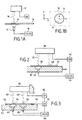
- the part 10 is provided with a circular hole 16 of center O, the hole 16 being linked to this part 10 and constituting the position reference.
- the detection device also includes a camera 17 arranged on the other side of the part 10 with respect to the laser beam 14 and capable to take an image of the periphery of the hole 16 and of the laser beam 14. From this image, a computing circuit 18 associated with the camera allows to calculate the components according to the orthogonal directions X and Y of the segment which joins the center O of the circle and the point of impact A and therefore of completely determine the relative positioning error.
- this device makes it possible to detect and measure two types of absolute positioning error depending on whether the laser beam constitutes the position reference and that the part 10 is mobile or that the part 10 constitutes the position reference by its hole circular 16, the laser beam 14 then being marred by an error possible position.
- the camera 17 must be able to detect the laser beam.
- FIG 2 there is shown the use of the device Figures 1A and 1B to the calibration of the laser beam with respect to the frame an exhibition facility.
- An optical unit 30 has been represented directing a laser beam 32 towards a part 34 integral with the frame 36 of the machine.
- the part 34 is for example constituted by a strip integral with the frame 36 and made of a material of great stability such than Invar.
- the strip 34 is provided with at least two orifices circular 38 and 40 of perfectly defined diameter. Ports 38 and 40 therefore constitute position references of the frame 36.
- the optical unit 30 is associated with a control unit 42 to control the point impact of the laser beam.
- the laser beam to be moved by scanning over a certain distance from the frame we can advantageously repeat the operation in relation to a second reference hole 40 formed in the strip 34 and by controlling the position of the laser beam with instructions corresponding to the position of this second hole 40.
- This error determination can be carried out for several holes arranged on strip 34.
- FIG. 3 we will describe an application of the device for detecting errors relating to the positioning of a printed circuit board 50 in a beam exposure machine laser.
- This panel 50 is provided with two holes for positioning 54 and 56.
- a optical unit 58 which controls the point of impact of a laser beam 60 in response to the instructions transmitted by a control circuit 62.
- the optical unit 58 is controlled so that the beam is focused at a point on the frame corresponding exactly to the position that the center of the positioning hole 54 should occupy.
- the camera 63 we take an image of the periphery of hole 54 and the impact of the laser beam 60 and the coordinates of this error are calculated in the calculation circuit 64.
- the block optic 58 is controlled so that a laser beam 60 'has a point of impact corresponding exactly to the theoretical position of the center of the second positioning hole 56 of the printed circuit board 50.
- a using a second camera 65 we take a second image corresponding to hole 56 and we transmit this second error of position at computation circuit 64.
- Rotation error can be measured by the angle between the straight line joining the centers of holes 54 and 56 and the straight line joining the two impact points of the laser beams.
- the error of rotational position is transmitted to the control circuit 66 actuators 68 to correct this error.
- the errors of position in X and Y are preferably directly transmitted to the circuits 62 of the optical unit 58.
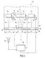
- FIG. 4 shows the case of an exposure machine 70 comprising several laser beams 72 1 , 72 2 , 72 3 , 72 4 produced by as many optical units 74 1 , 74 2 , 74 3 , 74 4 , each optical unit being controlled by a circuit 76.
- the frame 78 of the machine is equipped with an Invar 80 rule comprising as many series S 1 , S 2 , S 3 , S 4 of holes 82 of calibration that there are laser beams to calibrate.
- the holes of a series are respectively arranged opposite the zones Z 1 , Z 2 , Z 3 and Z 4 which the laser beam must scan; each series has for example 20 holes.
Abstract
Description
La présente invention a pour objet un dispositif de mesure d'erreur de position relative entre un faisceau laser et une pièce ainsi que des applications de ce dispositif à la réalisation d'une machine d'exposition de panneaux de circuit imprimé.The subject of the present invention is a measuring device relative position error between a laser beam and a workpiece as well as applications of this device to the realization of a machine exhibition of printed circuit boards.
On sait que, pour la fabrication de circuits imprimés par des procédés classiques, une des étapes consiste à recouvrir la couche conductrice du panneau de circuit imprimé d'une couche de matériau de réserve et à insoler cette couche de réserve à travers un cliché permettant d'obtenir la forme des pistes conductrices que l'on veut obtenir sur le circuit imprimé. Après insolation de cette couche de réserve, on procède à l'enlèvement des zones non-insolées correspondant aux portions de la couche conductrice que l'on veut enlever.It is known that, for the manufacture of printed circuits by one of the steps is to cover the layer conductor of the printed circuit board with a layer of material reserve and to insulate this reserve layer through a plate allowing to obtain the shape of the conductive tracks that we want to obtain on the printed circuit board. After exposure of this reserve layer, we proceed to the removal of the non-exposed areas corresponding to the portions of the conductive layer that we want to remove.
On sait également qu'il se développe une autre technique de réalisation de panneaux de circuit imprimé dans laquelle la couche de réserve est impressionnée localement par l'impact d'un faisceau laser. La position de l'impact du faisceau laser sur le panneau est commandée le plus souvent par un ensemble de balayage comportant un miroir polygonal rotatif combiné à un dispositif d'interruption commandé du faisceau laser qui est le plus souvent constitué par un modulateur acousto-optique.We also know that another technique is developing realization of printed circuit boards in which the layer of reserve is impressed locally by the impact of a laser beam. The position of the impact of the laser beam on the panel is controlled the more often by a scanning assembly comprising a mirror polygonal rotary combined with a controlled interruption device of the laser beam which is most often formed by a modulator acousto-optics.
D'autres techniques qui utilisent également un faisceau laser consistent, soit à réaliser directement l'ablation de la couche de réserve à l'aide d'un faisceau laser, soit à ne pas utiliser une couche de réserve et à réaliser directement l'ablation de la couche conductrice avec un faisceau laser.Other techniques that also use a laser beam consist either in directly carrying out the ablation of the reserve layer at using a laser beam, or not to use a reserve layer and to directly ablate the conductive layer with a beam laser.
Le nombre de points d'impact de faisceaux laser étant bien sûr très important pour réaliser avec la précision requise un panneau de circuit imprimé de grande dimension, il est intéressant de pouvoir diviser la surface du panneau de circuit imprimé en un certain nombre de zones et de balayer simultanément chacune de ces zones à l'aide d'un faisceau laser.The number of laser beam impact points being of course very important to achieve with the required precision a panel of large printed circuit, it is interesting to be able to divide the surface of the printed circuit board in a number of areas and simultaneously scan each of these areas using a beam laser.
Dans les machines qui permettent de réaliser cette opération et que l'on appellera ultérieurement machines d'exposition, il se pose deux problèmes principaux de positionnement relatif. D'une part, il est nécessaire de calibrer avec précision la position du faisceau laser ou de chaque faisceau laser par rapport au bâti de la machine d'exposition et d'autre part, il est nécessaire de positionner avec une grande précision sur le bâti de la machine le panneau de circuit imprimé destiné à être insolé par faisceau laser.In the machines which allow this operation to be carried out and which will later be called exposure machines, it arises two main problems of relative positioning. On the one hand, it is necessary to accurately calibrate the position of the laser beam or each laser beam relative to the frame of the exposure machine and on the other hand, it is necessary to position with great precision on the machine frame the printed circuit board intended to be exposed by laser beam.
En ce qui concerne la calibration du faisceau laser, on comprend que dans cette machine, celui-ci est dirigé vers le panneau de circuit imprimé à travers un bloc optique qui comporte un grand nombre de composants optiques. En outre, le balayage du panneau de circuit imprimé est obtenu le plus souvent à l'aide d'un miroir polygonal rotatif dont la rotation de chaque face définit en partie une longueur de balayage. Par ailleurs, le dessin qui doit être réalisé à l'aide du faisceau laser est défini à partir d'informations mémorisées qui donnent pour chaque point du panneau soit une information d'impact, soit une information d'absence d'impact.Regarding the calibration of the laser beam, we understands that in this machine, it is directed towards the panel printed circuit through an optical block which has a large number optical components. In addition, scanning the circuit panel print is most often obtained using a rotating polygon mirror the rotation of each face partly defines a length of scanning. In addition, the drawing which must be carried out using the beam laser is defined from stored information which gives for each point of the panel is either impact information or no impact information.
On comprend qu'au vu de tous ces éléments, quelle que soit la précision des réglages initiaux de ces différents composants, il est nécessaire avant chaque utilisation de la machine de vérifier la position réelle de l'impact d'un faisceau laser par rapport au bâti de la machine.We understand that in view of all these elements, whatever the precision of the initial settings of these different components, it is necessary before each use of the machine to check the position real impact of a laser beam relative to the machine frame.
En ce qui concerne le positionnement du panneau par rapport au bâti de la machine, on comprend que celui-ci doit également être réalisé avec une très grande précision, notamment dans le cas où les panneaux de circuit imprimé sont destinés à former les éléments constitutifs de circuit imprimé multicouches. On rappelle que le positionnement des panneaux de circuit imprimé par rapport au bâti de machine est le plus souvent obtenu à l'aide de trous circulaires réalisés en certains endroits du panneau défini avec précision.Regarding the positioning of the panel in relation to the machine frame, we understand that it must also be performed with great precision, especially in the case where the printed circuit boards are intended to form the elements constituting multilayer printed circuits. Remember that the positioning printed circuit boards relative to the machine frame is most often obtained using circular holes made in certain precisely defined areas of the panel.
Un objet de la présente invention est de fournir un dispositif de mesure d'erreur de position relative entre un faisceau laser et une pièce qui peut par exemple être le bâti d'une machine d'exposition ou un panneau de circuit imprimé qui permet de façon simple d'obtenir une détermination d'erreur avec une très grande précision.An object of the present invention is to provide a device for measurement of relative position error between a laser beam and a workpiece which can for example be the frame of an exhibition machine or a printed circuit board which allows a simple way to obtain a error determination with very high accuracy.
Pour atteindre ce but selon l'invention, le dispositif de mesure
d'erreur de position relative entre un faisceau laser et une pièce se
caractérise
en ce que ladite pièce est munie d'un orifice circulaire occupant
une position de référence par rapport à ladite pièce
et en ce qu'il comprend en outre :
- des moyens pour focaliser le faisceau laser dans le plan de ladite pièce,
- des moyens pour prendre une image dudit trou circulaire et du faisceau focalisé dans le plan de ladite pièce ; et
- des moyens pour calculer les composantes du segment joignant ledit point d'impact et le centre dudit trou.
in that said part is provided with a circular orifice occupying a reference position with respect to said part
and in that it further comprises:
- means for focusing the laser beam in the plane of said part,
- means for taking an image of said circular hole and of the beam focused in the plane of said part; and
- means for calculating the components of the segment joining said point of impact and the center of said hole.
On comprend que grâce à l'invention, on obtient effectivement une détermination très précise de l'erreur notamment du fait que le positionnement des moyens de prise d'image, par exemple une caméra, n'a pas besoin d'être réalisé avec précision puisqu'il suffit qu'ils permettent d'obtenir simultanément l'image de la périphérie du trou circulaire et l'image de l'impact du faisceau laser.We understand that thanks to the invention, we actually obtain a very precise determination of the error, in particular because the positioning of the image taking means, for example a camera, does not need to be performed with precision since it suffices that they allow simultaneously obtain the image of the periphery of the circular hole and the image of the impact of the laser beam.
Un autre objet de l'invention est de fournir une application du dispositif défini ci-dessus à la réalisation d'une machine d'exposition de panneaux de circuit imprimé pour réaliser le positionnement du panneau de circuit imprimé par rapport au bâti de la machine.Another object of the invention is to provide an application of the device defined above for the production of an exposure machine for printed circuit boards for positioning the panel circuit board in relation to the machine frame.
Cette application se caractérise en ce que ladite machine comprend en outre :
- des moyens pour focaliser ledit faisceau laser successivement en deux points du bâti correspondant qui devraient être occupés par les centres des deux trous circulaires,
- des moyens par caméra pour prendre une image des deux trous et des points d'impact de faisceau laser,
- des moyens pour calculer à partir de chacune desdites images les composantes du segment joignant le centre du cercle au point d'impact du faisceau par quoi on obtient deux ensembles d'informations d'erreur de position du panneau,
- des moyens pour déplacer ledit panneau par rapport au bâti au moins en rotation, et des moyens pour commander les moyens de déplacement et les moyens de focalisation du faisceau laser en fonction des deux ensembles d'informations d'erreur de position du panneau.
- means for focusing said laser beam successively at two points of the corresponding frame which should be occupied by the centers of the two circular holes,
- means by camera for taking an image of the two holes and of the laser beam impact points,
- means for calculating from each of said images the components of the segment joining the center of the circle to the point of impact of the beam by which two sets of error information of position of the panel are obtained,
- means for moving said panel relative to the frame at least in rotation, and means for controlling the means for moving and the means for focusing the laser beam as a function of the two sets of position error information of the panel.
On comprend que dans ce cas, la référence est constituée par le point d'impact du faisceau laser et que l'élément dont on veut corriger l'erreur de position est le panneau avec ses deux trous de positionnement.We understand that in this case, the reference is constituted by the point of impact of the laser beam and that the element which we want to correct the position error is the panel with its two positioning holes.
Un autre objet de l'invention est d'appliquer le dispositif de détection défini ci-dessus à la calibration du faisceau laser d'une machine d'exposition de panneaux de circuit imprimé. Cette application se caractérise en ce qu'elle comprend en outre :
- au moins une pièce solidaire dudit bâti, ladite pièce comportant au moins un trou circulaire dont le centre constitue un point de référence du bâti,
- des moyens pour commander les moyens de déflexion de faisceau par des informations de position correspondant à la position du centre dudit cercle,
- des moyens par caméra pour prendre une image dudit trou circulaire et du point d'impact effectif du faisceau laser dans ledit trou,
- des moyens pour calculer les composantes du segment joignant le centre dudit trou au point d'impact du faisceau laser, et des moyens pour transmettre aux moyens de commande des moyens de déflexion lesdites composantes.
- at least one piece integral with said frame, said piece comprising at least one circular hole whose center constitutes a reference point of the frame,
- means for controlling the beam deflection means by position information corresponding to the position of the center of said circle,
- camera means for taking an image of said circular hole and of the effective point of impact of the laser beam in said hole,
- means for calculating the components of the segment joining the center of said hole at the point of impact of the laser beam, and means for transmitting said components to the deflection means.
On comprend que dans ce cas, la référence de position est constituée par la pièce munie du trou circulaire et l'élément dont on doit déterminer l'erreur de position est le point d'impact du faisceau laser.We understand that in this case, the position reference is consisting of the part provided with the circular hole and the element to be determining the position error is the point of impact of the laser beam.
D'autres caractéristiques et avantages de l'invention
apparaítront mieux à la lecture de la description qui suit de plusieurs
modes de réalisation de l'invention donnés à titre d'exemples non
limitatifs. La description se réfère aux figures annexées sur lesquelles :
En se référant tout d'abord aux figures 1A et 1B, on va décrire
le dispositif de détection et de mesure d'erreur de positionnement relatif
d'un faisceau laser et d'une pièce. Sur ces figures, on a représenté une
pièce 10 et un système optique 12 pour émettre un faisceau laser 14 vers
la pièce 10.Referring first to Figures 1A and 1B, we will describe
the device for detecting and measuring relative positioning error
a laser beam and a part. In these figures, a
La pièce 10 est munie d'un trou circulaire 16 de centre O, le
trou 16 étant lié à cette pièce 10 et en constituant la référence de position.
Le dispositif de détection comporte également une caméra 17 disposée
de l'autre côté de la pièce 10 par rapport au faisceau laser 14 et capable
de prendre une image de la périphérie du trou 16 et du faisceau laser 14.
A partir de cette image, un circuit de calcul 18 associé à la caméra permet
de calculer les composantes selon les directions orthogonales X et Y du
segment qui joint le centre O du cercle et le point d'impact A et donc de
déterminer complètement l'erreur de positionnement relative.The
Comme on l'a déjà exposé, ce dispositif permet de détecter et
de mesurer deux types d'erreur de positionnement absolu selon que le
faisceau laser constitue la référence de position et que la pièce 10 est
mobile ou que la pièce 10 constitue la référence de position par son trou
circulaire 16, le faisceau laser 14 étant alors entaché d'une erreur
éventuelle de position.As already explained, this device makes it possible to detect and
measure two types of absolute positioning error depending on whether the
laser beam constitutes the position reference and that the
Il faut bien sûr que la caméra 17 soit capable de détecter le
faisceau laser. On pourra choisir une caméra CCD pourvue d'objectifs
adaptés aux longueurs d'onde du faisceau laser.Of course, the
Sur la figure 2, on a représenté l'utilisation du dispositif des
figures 1A et 1B à la calibration du faisceau laser par rapport au bâti
d'une installation d'exposition. On a représenté un bloc optique 30
dirigeant un faisceau laser 32 vers une pièce 34 solidaire du bâti 36 de la
machine. La pièce 34 est par exemple constituée par une réglette
solidaire du bâti 36 et réalisée en un matériau d'une grande stabilité telle
que de l'Invar. La réglette 34 est munie d'au moins deux orifices
circulaires 38 et 40 de diamètre parfaitement défini. Les orifices 38 et 40
constituent donc des références de position du bâti 36. Le bloc optique 30
est associé à un ensemble de commande 42 pour contrôler le point
d'impact du faisceau laser.In Figure 2, there is shown the use of the device
Figures 1A and 1B to the calibration of the laser beam with respect to the frame
an exhibition facility. An
Pour effectuer la calibration du faisceau laser, on envoie à
l'aide du circuit de commande 42 vers le bloc optique 30 des instructions
de positionnement du faisceau laser correspondant à la position exacte du
trou 34. A l'aide d'une caméra 44, on procède à la prise d'image du
trou 38 et du faisceau 32. Le circuit 46 associé à la caméra 44 calcule les
erreurs de position comme indiqué précédemment. Du fait que le faisceau
laser est positionné en partie à l'aide d'instructions mémorisées dans ses
circuits de commande, le calcul d'erreur pourrait être utilisé pour corriger
les instructions de commande de positionnement du faisceau laser.To calibrate the laser beam, send to
using the
Le faisceau laser devant être déplacé par balayage sur une
certaine distance par rapport au bâti, on peut avantageusement répéter
l'opération en relation avec un deuxième trou de référence 40 ménagé
dans la réglette 34 et en commandant la position du faisceau laser avec
des instructions correspondant à la position de ce deuxième trou 40. Cette
détermination d'erreur peut être réalisée pour plusieurs trous disposés sur
la réglette 34. Ces différentes mesures d'erreur pour différentes positions
repérées par la réglette permettent de calculer un polynôme de correction
d'erreurs qui permettra de corriger les instructions de balayage par le
faisceau pour chaque position de balayage.The laser beam to be moved by scanning over a
certain distance from the frame, we can advantageously repeat
the operation in relation to a
En se référant maintenant à la figure 3, on va décrire une application
du dispositif de détection d'erreurs relatives au positionnement d'un
panneau de circuit imprimé 50 dans une machine d'insolation par faisceau
laser. Sur cette figure, on a représenté un bâti 52 de la machine sur lequel
est disposé le panneau 50. Ce panneau 50 est pourvu de deux trous de
positionnement 54 et 56. Sur cette figure, on a également représenté un
bloc optique 58 qui commande le point d'impact d'un faisceau laser 60 en
réponse aux instructions transmises par un circuit de commande 62.Referring now to Figure 3, we will describe an application
of the device for detecting errors relating to the positioning of a
printed
Pour réaliser le positionnement du panneau 50 par rapport au
bâti 52, on commande le bloc optique 58 de telle façon que le faisceau
soit focalisé en un point du bâti correspondant exactement à la position
que devrait occuper le centre du trou de positionnement 54. A l'aide de la
caméra 63, on prend une image de la périphérie du trou 54 et de l'impact
du faisceau laser 60 et l'on calcule les coordonnées de cette erreur dans
le circuit de calcul 64. Pour finaliser l'opération de positionnement, le bloc
optique 58 est commandé pour qu'un faisceau laser 60' ait un point
d'impact correspondant exactement à la position théorique du centre du
deuxième trou de positionnement 56 du panneau de circuit imprimé 50. A
l'aide d'une deuxième caméra 65, on prend une deuxième image
correspondant au trou 56 et on transmet cette deuxième erreur de
position au circuit de calcul 64. Ces deux erreurs de position permettent
de déterminer des erreurs de position du panneau selon deux directions
orthogonales X et Y et en rotation. L'erreur en rotation peut être mesurée
par l'angle entre la droite joignant les centres des trous 54 et 56 et la
droite joignant les deux points d'impact des faisceaux laser. L'erreur de
position en rotation est transmise au circuit de commande 66
d'actuateurs 68 permettant de corriger cette erreur. Les erreurs de
position en X et Y sont de préférence directement transmises aux circuits
de commande 62 du bloc optique 58.To position the
Sur la figure 4, on a représenté le cas d'une machine
d'exposition 70 comportant plusieurs faisceaux laser 721, 722, 723, 724
produits par autant de blocs optiques 741, 742, 743, 744, chaque bloc
optique étant commandé par un circuit 76. Pour la calibration des
faisceaux laser, le bâti 78 de la machine est équipé d'une règle en Invar
80 comportant autant de séries S1, S2, S3, S4 de trous 82 de calibration
qu'il y a de faisceaux laser à calibrer. Les trous d'une série sont
respectivement disposés en regard des zones Z1, Z2, Z3 et Z4 que doit
balayer le faisceau laser ; chaque série comporte par exemple 20 trous.FIG. 4 shows the case of an
A l'aide d'une caméra mobile 84, on prend successivement
pour chaque trou 82 de chaque série de trous, les images des trous et du
faisceau laser et chaque série de trous. Le circuit de calcul 86 élabore
alors, pour chaque faisceau laser, un polynôme de correction qui est
transmis aux circuits de commande 76 des blocs optiques.Using a mobile camera 84, we successively take
for each
Claims (6)
en ce que ladite pièce est munie d'un orifice circulaire occupant une position de référence par rapport à ladite pièce
et en ce qu'il comprend en outre :
in that said part is provided with a circular orifice occupying a reference position with respect to said part
and in that it further comprises:
ladite machine comprend :
en ce que lesdits moyens de calcul déterminent une fonction polynomiale de correction de position pour chaque série d'images associée à une série de trous.Application according to claim 5, characterized in that
said machine comprises:
in that said calculating means determine a polynomial position correction function for each series of images associated with a series of holes.
Applications Claiming Priority (2)
| Application Number | Priority Date | Filing Date | Title |
|---|---|---|---|
| FR9913725 | 1999-11-03 | ||
| FR9913725A FR2800565B1 (en) | 1999-11-03 | 1999-11-03 | RELATIVE POSITION ERROR MEASURING DEVICE |
Publications (2)
| Publication Number | Publication Date |
|---|---|
| EP1098556A1 true EP1098556A1 (en) | 2001-05-09 |
| EP1098556B1 EP1098556B1 (en) | 2007-02-07 |
Family
ID=9551646
Family Applications (1)
| Application Number | Title | Priority Date | Filing Date |
|---|---|---|---|
| EP00402847A Expired - Lifetime EP1098556B1 (en) | 1999-11-03 | 2000-10-16 | Device for measuring a positioning error |
Country Status (11)
| Country | Link |
|---|---|
| US (1) | US6683684B1 (en) |
| EP (1) | EP1098556B1 (en) |
| JP (1) | JP2001188007A (en) |
| KR (1) | KR20010060196A (en) |
| CN (1) | CN1220116C (en) |
| AT (1) | ATE353538T1 (en) |
| CA (1) | CA2324913A1 (en) |
| DE (1) | DE60033258T2 (en) |
| ES (1) | ES2281329T3 (en) |
| FR (1) | FR2800565B1 (en) |
| TW (1) | TW556456B (en) |
Cited By (1)
| Publication number | Priority date | Publication date | Assignee | Title |
|---|---|---|---|---|
| CN102865815A (en) * | 2012-09-24 | 2013-01-09 | 上海功源电子科技有限公司 | Novel positioning compensation method for PCB by single vision camera |
Families Citing this family (15)
| Publication number | Priority date | Publication date | Assignee | Title |
|---|---|---|---|---|
| IL161274A0 (en) * | 2001-10-10 | 2004-09-27 | Accent Optical Tech Inc | Determination of center of focus by cross-section analysis |
| JP4338577B2 (en) * | 2004-04-28 | 2009-10-07 | 株式会社ブイ・テクノロジー | Exposure equipment |
| JP4391545B2 (en) * | 2007-03-30 | 2009-12-24 | 日立ビアメカニクス株式会社 | Work processing machine |
| CN101450788B (en) * | 2007-12-05 | 2011-04-13 | 中国科学院微电子研究所 | Quartz wafer deep micropore processing equipment and method |
| CN104378916B (en) * | 2013-08-13 | 2018-04-03 | 达观科技有限公司 | Object bearing calibration |
| CN104897070B (en) * | 2014-03-07 | 2018-04-17 | 达观科技有限公司 | Process the detection method of object base specification |
| JP6483536B2 (en) * | 2015-06-05 | 2019-03-13 | 株式会社アドテックエンジニアリング | Pattern drawing apparatus and pattern drawing method |
| CN105043269B (en) * | 2015-07-08 | 2017-09-29 | 上海与德通讯技术有限公司 | The measuring method and electronic equipment of a kind of dimension of object |
| CN106767556B (en) * | 2016-12-26 | 2023-06-06 | 重庆越发机械制造有限公司 | Concentricity detection equipment for high-precision gear shifting fork |
| WO2019048198A1 (en) * | 2017-09-11 | 2019-03-14 | Asml Netherlands B.V. | Lithographic apparatus and method |
| CN109209546B (en) * | 2018-09-30 | 2019-12-27 | 东风汽车集团有限公司 | Clearance adjusting device and method of continuous variable valve lift mechanism |
| CN112179286B (en) * | 2020-08-18 | 2021-12-21 | 江苏瑞尔隆盛叶轮科技有限公司 | Clamp special for GOM three-dimensional optical scanner |
| CN111928873A (en) * | 2020-09-28 | 2020-11-13 | 快克智能装备股份有限公司 | Method for calibrating height measurement center and camera center |
| CN112857220B (en) * | 2021-01-13 | 2022-08-09 | 德阳市产品质量监督检验所 | Detection structure of power generation equipment parts |
| CN113207232A (en) * | 2021-04-30 | 2021-08-03 | 东莞市五株电子科技有限公司 | Three-dimensional PCB manufacturing method and PCB |
Citations (3)
| Publication number | Priority date | Publication date | Assignee | Title |
|---|---|---|---|---|
| DD241562A1 (en) * | 1985-10-10 | 1986-12-17 | Robotron Bueromasch | MESSTECHNICAL ARRANGEMENT FOR MONITORING THE CUTTING PROCESS FOR LASER SEPARATION |
| EP0618505A1 (en) * | 1993-03-31 | 1994-10-05 | Automa-Tech | Device for exposing to light a double sided circuit board plate through printing plates |
| EP0827035A2 (en) * | 1996-08-26 | 1998-03-04 | Demminer Maschinen Technik GmbH | Method and apparatus for aligning photoprinting plates in a production line |
Family Cites Families (2)
| Publication number | Priority date | Publication date | Assignee | Title |
|---|---|---|---|---|
| DE241562C (en) | 1909-07-31 | 1911-12-05 | ||
| US5264869A (en) * | 1991-08-19 | 1993-11-23 | Xerox Corporation | Electro-optical control apparatus and system for spot position control in an optical output device |
-
1999
- 1999-11-03 FR FR9913725A patent/FR2800565B1/en not_active Expired - Fee Related
-
2000
- 2000-10-16 EP EP00402847A patent/EP1098556B1/en not_active Expired - Lifetime
- 2000-10-16 US US09/688,900 patent/US6683684B1/en not_active Expired - Fee Related
- 2000-10-16 DE DE60033258T patent/DE60033258T2/en not_active Expired - Fee Related
- 2000-10-16 ES ES00402847T patent/ES2281329T3/en not_active Expired - Lifetime
- 2000-10-16 AT AT00402847T patent/ATE353538T1/en not_active IP Right Cessation
- 2000-10-23 KR KR1020000062366A patent/KR20010060196A/en not_active Application Discontinuation
- 2000-10-31 CA CA002324913A patent/CA2324913A1/en not_active Abandoned
- 2000-11-02 JP JP2000336242A patent/JP2001188007A/en not_active Withdrawn
- 2000-11-02 TW TW089123119A patent/TW556456B/en not_active IP Right Cessation
- 2000-11-03 CN CNB001338080A patent/CN1220116C/en not_active Expired - Fee Related
Patent Citations (3)
| Publication number | Priority date | Publication date | Assignee | Title |
|---|---|---|---|---|
| DD241562A1 (en) * | 1985-10-10 | 1986-12-17 | Robotron Bueromasch | MESSTECHNICAL ARRANGEMENT FOR MONITORING THE CUTTING PROCESS FOR LASER SEPARATION |
| EP0618505A1 (en) * | 1993-03-31 | 1994-10-05 | Automa-Tech | Device for exposing to light a double sided circuit board plate through printing plates |
| EP0827035A2 (en) * | 1996-08-26 | 1998-03-04 | Demminer Maschinen Technik GmbH | Method and apparatus for aligning photoprinting plates in a production line |
Cited By (2)
| Publication number | Priority date | Publication date | Assignee | Title |
|---|---|---|---|---|
| CN102865815A (en) * | 2012-09-24 | 2013-01-09 | 上海功源电子科技有限公司 | Novel positioning compensation method for PCB by single vision camera |
| CN102865815B (en) * | 2012-09-24 | 2015-01-07 | 上海功源电子科技有限公司 | Novel positioning compensation method for PCB by single vision camera |
Also Published As
| Publication number | Publication date |
|---|---|
| DE60033258T2 (en) | 2007-11-22 |
| EP1098556B1 (en) | 2007-02-07 |
| FR2800565A1 (en) | 2001-05-04 |
| CA2324913A1 (en) | 2001-05-03 |
| CN1220116C (en) | 2005-09-21 |
| ES2281329T3 (en) | 2007-10-01 |
| ATE353538T1 (en) | 2007-02-15 |
| JP2001188007A (en) | 2001-07-10 |
| DE60033258D1 (en) | 2007-03-22 |
| KR20010060196A (en) | 2001-07-06 |
| FR2800565B1 (en) | 2002-10-25 |
| CN1295268A (en) | 2001-05-16 |
| US6683684B1 (en) | 2004-01-27 |
| TW556456B (en) | 2003-10-01 |
Similar Documents
| Publication | Publication Date | Title |
|---|---|---|
| EP1098556B1 (en) | Device for measuring a positioning error | |
| EP0113633B1 (en) | Method and device for the optical alignment of motives in close planes in an exposing apparatus provided with a diverging radiation source | |
| US20100020180A1 (en) | Alignment metrology and resolution measurement system for imaging arrays | |
| FR2916534A1 (en) | METHOD AND DEVICE FOR NON-CONTACT MEASUREMENT OF OSCILLATIONS OF AN OBJECT | |
| US7692128B2 (en) | Focus control method for an optical apparatus which inspects a photo-mask or the like | |
| EP2516100B1 (en) | Method of ablating a three-dimensional surface using a laser ablation device and through the use of a calibration step; device for implementing such a method | |
| FR2534017A1 (en) | METHOD AND APPARATUS FOR REALIZING STATIC ALIGNMENT OF TREES AND CONTROLLING THE ALIGNMENT | |
| EP2629049A2 (en) | Sensor | |
| US8294902B2 (en) | Measuring method and measuring device for measuring a shape of a measurement surface using a reference standard for calibration | |
| US20060018560A1 (en) | Exposure device and exposure method | |
| EP0618505B1 (en) | Device for exposing to light a double sided circuit board plate through printing plates | |
| EP0015789B1 (en) | Optical photorepeating projection device | |
| FR2858680A1 (en) | STABILIZED PLATFORM SYSTEM | |
| EP0156683B1 (en) | Apparatus for optical micro-lithography with a local alignment system | |
| JP6361273B2 (en) | Substrate processing apparatus and device manufacturing method | |
| CN103365115A (en) | Exposure apparatus, method of controlling the same and method of manufacturing device | |
| KR100950589B1 (en) | Linnik interferometry having tilt unit | |
| FR2693565A1 (en) | Method of setting a photolithographic exposure machine and associated device | |
| FR2841993A1 (en) | METHOD AND APPARATUS FOR ALIGNING A DIFFRACTION ARRAY | |
| JP7076042B2 (en) | Laser triangulation equipment and calibration method | |
| JP4618720B2 (en) | Unevenness inspection apparatus and unevenness inspection method | |
| FR3081593A1 (en) | METHOD FOR CALIBRATING A CAMERA OF A THREE-DIMENSIONAL IMAGE DETERMINING SYSTEM AND CALIBRATION MIRE | |
| US6636369B2 (en) | Device for maintaining alignment between a focal point of a laser beam and a slit aperture | |
| BE1015708A3 (en) | Method for measuring the height of spheres or hemispheres. | |
| JP6750712B2 (en) | Substrate processing apparatus and device manufacturing method |
Legal Events
| Date | Code | Title | Description |
|---|---|---|---|
| PUAI | Public reference made under article 153(3) epc to a published international application that has entered the european phase |
Free format text: ORIGINAL CODE: 0009012 |
|
| AK | Designated contracting states |
Kind code of ref document: A1 Designated state(s): AT BE CH CY DE DK ES FI FR GB GR IE IT LI LU MC NL PT SE |
|
| AX | Request for extension of the european patent |
Free format text: AL;LT;LV;MK;RO;SI |
|
| 17P | Request for examination filed |
Effective date: 20010716 |
|
| AKX | Designation fees paid |
Free format text: AT BE CH CY DE DK ES FI FR GB GR IE IT LI LU MC NL PT SE |
|
| GRAP | Despatch of communication of intention to grant a patent |
Free format text: ORIGINAL CODE: EPIDOSNIGR1 |
|
| GRAS | Grant fee paid |
Free format text: ORIGINAL CODE: EPIDOSNIGR3 |
|
| GRAA | (expected) grant |
Free format text: ORIGINAL CODE: 0009210 |
|
| AK | Designated contracting states |
Kind code of ref document: B1 Designated state(s): AT BE CH CY DE DK ES FI FR GB GR IE IT LI LU MC NL PT SE |
|
| PG25 | Lapsed in a contracting state [announced via postgrant information from national office to epo] |
Ref country code: NL Free format text: LAPSE BECAUSE OF FAILURE TO SUBMIT A TRANSLATION OF THE DESCRIPTION OR TO PAY THE FEE WITHIN THE PRESCRIBED TIME-LIMIT Effective date: 20070207 Ref country code: IE Free format text: LAPSE BECAUSE OF FAILURE TO SUBMIT A TRANSLATION OF THE DESCRIPTION OR TO PAY THE FEE WITHIN THE PRESCRIBED TIME-LIMIT Effective date: 20070207 Ref country code: FI Free format text: LAPSE BECAUSE OF FAILURE TO SUBMIT A TRANSLATION OF THE DESCRIPTION OR TO PAY THE FEE WITHIN THE PRESCRIBED TIME-LIMIT Effective date: 20070207 Ref country code: DK Free format text: LAPSE BECAUSE OF FAILURE TO SUBMIT A TRANSLATION OF THE DESCRIPTION OR TO PAY THE FEE WITHIN THE PRESCRIBED TIME-LIMIT Effective date: 20070207 |
|
| REG | Reference to a national code |
Ref country code: GB Ref legal event code: FG4D Free format text: NOT ENGLISH |
|
| REG | Reference to a national code |
Ref country code: CH Ref legal event code: EP |
|
| REG | Reference to a national code |
Ref country code: IE Ref legal event code: FG4D Free format text: LANGUAGE OF EP DOCUMENT: FRENCH |
|
| REF | Corresponds to: |
Ref document number: 60033258 Country of ref document: DE Date of ref document: 20070322 Kind code of ref document: P |
|
| PG25 | Lapsed in a contracting state [announced via postgrant information from national office to epo] |
Ref country code: SE Free format text: LAPSE BECAUSE OF FAILURE TO SUBMIT A TRANSLATION OF THE DESCRIPTION OR TO PAY THE FEE WITHIN THE PRESCRIBED TIME-LIMIT Effective date: 20070507 |
|
| GBT | Gb: translation of ep patent filed (gb section 77(6)(a)/1977) |
Effective date: 20070413 |
|
| PG25 | Lapsed in a contracting state [announced via postgrant information from national office to epo] |
Ref country code: PT Free format text: LAPSE BECAUSE OF FAILURE TO SUBMIT A TRANSLATION OF THE DESCRIPTION OR TO PAY THE FEE WITHIN THE PRESCRIBED TIME-LIMIT Effective date: 20070709 |
|
| NLV1 | Nl: lapsed or annulled due to failure to fulfill the requirements of art. 29p and 29m of the patents act | ||
| REG | Reference to a national code |
Ref country code: IE Ref legal event code: FD4D |
|
| REG | Reference to a national code |
Ref country code: ES Ref legal event code: FG2A Ref document number: 2281329 Country of ref document: ES Kind code of ref document: T3 |
|
| PLBE | No opposition filed within time limit |
Free format text: ORIGINAL CODE: 0009261 |
|
| STAA | Information on the status of an ep patent application or granted ep patent |
Free format text: STATUS: NO OPPOSITION FILED WITHIN TIME LIMIT |
|
| 26N | No opposition filed |
Effective date: 20071108 |
|
| PGFP | Annual fee paid to national office [announced via postgrant information from national office to epo] |
Ref country code: ES Payment date: 20071017 Year of fee payment: 8 Ref country code: DE Payment date: 20071010 Year of fee payment: 8 |
|
| PGFP | Annual fee paid to national office [announced via postgrant information from national office to epo] |
Ref country code: AT Payment date: 20070917 Year of fee payment: 8 Ref country code: IT Payment date: 20071020 Year of fee payment: 8 |
|
| BERE | Be: lapsed |
Owner name: AUTOMA-TECH Effective date: 20071031 |
|
| PG25 | Lapsed in a contracting state [announced via postgrant information from national office to epo] |
Ref country code: GR Free format text: LAPSE BECAUSE OF FAILURE TO SUBMIT A TRANSLATION OF THE DESCRIPTION OR TO PAY THE FEE WITHIN THE PRESCRIBED TIME-LIMIT Effective date: 20070508 |
|
| PGFP | Annual fee paid to national office [announced via postgrant information from national office to epo] |
Ref country code: GB Payment date: 20071016 Year of fee payment: 8 Ref country code: FR Payment date: 20071026 Year of fee payment: 8 |
|
| PG25 | Lapsed in a contracting state [announced via postgrant information from national office to epo] |
Ref country code: MC Free format text: LAPSE BECAUSE OF NON-PAYMENT OF DUE FEES Effective date: 20071031 |
|
| REG | Reference to a national code |
Ref country code: CH Ref legal event code: PL |
|
| PG25 | Lapsed in a contracting state [announced via postgrant information from national office to epo] |
Ref country code: LI Free format text: LAPSE BECAUSE OF NON-PAYMENT OF DUE FEES Effective date: 20071031 Ref country code: CH Free format text: LAPSE BECAUSE OF NON-PAYMENT OF DUE FEES Effective date: 20071031 |
|
| PG25 | Lapsed in a contracting state [announced via postgrant information from national office to epo] |
Ref country code: BE Free format text: LAPSE BECAUSE OF NON-PAYMENT OF DUE FEES Effective date: 20071031 |
|
| GBPC | Gb: european patent ceased through non-payment of renewal fee |
Effective date: 20081016 |
|
| REG | Reference to a national code |
Ref country code: FR Ref legal event code: ST Effective date: 20090630 |
|
| PG25 | Lapsed in a contracting state [announced via postgrant information from national office to epo] |
Ref country code: CY Free format text: LAPSE BECAUSE OF FAILURE TO SUBMIT A TRANSLATION OF THE DESCRIPTION OR TO PAY THE FEE WITHIN THE PRESCRIBED TIME-LIMIT Effective date: 20070207 |
|
| PG25 | Lapsed in a contracting state [announced via postgrant information from national office to epo] |
Ref country code: LU Free format text: LAPSE BECAUSE OF NON-PAYMENT OF DUE FEES Effective date: 20071016 Ref country code: IT Free format text: LAPSE BECAUSE OF NON-PAYMENT OF DUE FEES Effective date: 20081016 Ref country code: DE Free format text: LAPSE BECAUSE OF NON-PAYMENT OF DUE FEES Effective date: 20090501 Ref country code: AT Free format text: LAPSE BECAUSE OF NON-PAYMENT OF DUE FEES Effective date: 20081016 |
|
| PG25 | Lapsed in a contracting state [announced via postgrant information from national office to epo] |
Ref country code: FR Free format text: LAPSE BECAUSE OF NON-PAYMENT OF DUE FEES Effective date: 20081031 |
|
| PG25 | Lapsed in a contracting state [announced via postgrant information from national office to epo] |
Ref country code: GB Free format text: LAPSE BECAUSE OF NON-PAYMENT OF DUE FEES Effective date: 20081016 |
|
| REG | Reference to a national code |
Ref country code: ES Ref legal event code: FD2A Effective date: 20081017 |
|
| PG25 | Lapsed in a contracting state [announced via postgrant information from national office to epo] |
Ref country code: ES Free format text: LAPSE BECAUSE OF NON-PAYMENT OF DUE FEES Effective date: 20081017 |