EP1098441A2 - Potentiometric DAC having improved ratiometric output voltage stability - Google Patents
Potentiometric DAC having improved ratiometric output voltage stability Download PDFInfo
- Publication number
- EP1098441A2 EP1098441A2 EP00309743A EP00309743A EP1098441A2 EP 1098441 A2 EP1098441 A2 EP 1098441A2 EP 00309743 A EP00309743 A EP 00309743A EP 00309743 A EP00309743 A EP 00309743A EP 1098441 A2 EP1098441 A2 EP 1098441A2
- Authority
- EP
- European Patent Office
- Prior art keywords
- switches
- resistors
- string
- capacitor
- voltage
- Prior art date
- Legal status (The legal status is an assumption and is not a legal conclusion. Google has not performed a legal analysis and makes no representation as to the accuracy of the status listed.)
- Withdrawn
Links
- 239000003990 capacitor Substances 0.000 claims abstract description 88
- 238000005070 sampling Methods 0.000 claims description 25
- 238000010079 rubber tapping Methods 0.000 claims description 18
- 238000012935 Averaging Methods 0.000 claims description 13
- 230000000694 effects Effects 0.000 claims description 8
- 238000000034 method Methods 0.000 claims description 8
- 238000006243 chemical reaction Methods 0.000 claims description 2
- 230000005669 field effect Effects 0.000 claims description 2
- 230000008901 benefit Effects 0.000 description 4
- 238000010586 diagram Methods 0.000 description 3
- 230000002123 temporal effect Effects 0.000 description 2
- 230000009286 beneficial effect Effects 0.000 description 1
- 230000003139 buffering effect Effects 0.000 description 1
- 229920005994 diacetyl cellulose Polymers 0.000 description 1
- 239000012535 impurity Substances 0.000 description 1
- 238000004519 manufacturing process Methods 0.000 description 1
- 238000012986 modification Methods 0.000 description 1
- 230000004048 modification Effects 0.000 description 1
Images

Classifications
-
- H—ELECTRICITY
- H03—ELECTRONIC CIRCUITRY
- H03M—CODING; DECODING; CODE CONVERSION IN GENERAL
- H03M1/00—Analogue/digital conversion; Digital/analogue conversion
- H03M1/06—Continuously compensating for, or preventing, undesired influence of physical parameters
- H03M1/0617—Continuously compensating for, or preventing, undesired influence of physical parameters characterised by the use of methods or means not specific to a particular type of detrimental influence
- H03M1/0634—Continuously compensating for, or preventing, undesired influence of physical parameters characterised by the use of methods or means not specific to a particular type of detrimental influence by averaging out the errors, e.g. using sliding scale
- H03M1/0656—Continuously compensating for, or preventing, undesired influence of physical parameters characterised by the use of methods or means not specific to a particular type of detrimental influence by averaging out the errors, e.g. using sliding scale in the time domain, e.g. using intended jitter as a dither signal
- H03M1/066—Continuously compensating for, or preventing, undesired influence of physical parameters characterised by the use of methods or means not specific to a particular type of detrimental influence by averaging out the errors, e.g. using sliding scale in the time domain, e.g. using intended jitter as a dither signal by continuously permuting the elements used, i.e. dynamic element matching
- H03M1/0663—Continuously compensating for, or preventing, undesired influence of physical parameters characterised by the use of methods or means not specific to a particular type of detrimental influence by averaging out the errors, e.g. using sliding scale in the time domain, e.g. using intended jitter as a dither signal by continuously permuting the elements used, i.e. dynamic element matching using clocked averaging
-
- H—ELECTRICITY
- H03—ELECTRONIC CIRCUITRY
- H03M—CODING; DECODING; CODE CONVERSION IN GENERAL
- H03M1/00—Analogue/digital conversion; Digital/analogue conversion
- H03M1/66—Digital/analogue converters
- H03M1/74—Simultaneous conversion
- H03M1/76—Simultaneous conversion using switching tree
- H03M1/765—Simultaneous conversion using switching tree using a single level of switches which are controlled by unary decoded digital signals
Definitions
- This invention relates generally to potentiometric digital to analog converters (DAC's).
- DAC's are widely used in the electronic industry.
- ASIC's application specific integrated circuits
- many application specific integrated circuits (ASIC's) employ one or more DAC's of the type shown in Fig. 1 in which a string of serially connected resistors connected between two voltage supplies V DD and V SS has a tap provided at a selected point in the string, at R DX in the example, to provide a voltage of a certain fraction of the range between the two voltage supplies at V OUT .
- ASIC's application specific integrated circuits
- Fig. 1 many application specific integrated circuits (ASIC's) employ one or more DAC's of the type shown in Fig. 1 in which a string of serially connected resistors connected between two voltage supplies V DD and V SS has a tap provided at a selected point in the string, at R DX in the example, to provide a voltage of a certain fraction of the range between the two voltage supplies at V OUT .
- This simple arrangement has provided a relatively stable ratiometric output
- the normalized magnitude, that is, the number of LSB steps, of this drift can be significantly larger for DAC's which span only a fraction of the supply range. Slight differences in impurity doping or in stress relief with change in temperature and over time can cause drift which will change the fractional output of a DAC.
- An object of the invention is to provide a potentiometric DAC having improved output voltage stability. Another object is the provision of a potentiometric DAC which has a ratiometric output voltage having enhanced insensitivity to variability caused by manufacturing, both thermal and temporal, in individual resistor values. Yet another object of the invention is the provision of a potentiometric DAC free of the limitations of the prior art discussed above.
- the invention provides a potentiometric digital-to-analogue converter (DAC) including:
- the network of switches includes a first switch connected to the first end of the string of resistors, a second switch connected to the second end of the string of resistors, a third switch connected to the first end of the string of resistors and a fourth switch connected to the second end of the string of resistors, the first and second switches being operable as a pair to effect current flow through the string of resistors in the forward sense and the third and fourth switches operable as a pair to effect current flow through the string of resistors in the reverse sense.
- the sampling circuit means includes fifth and sixth switches capable of connecting the sampling circuit means to selected tapping points of the string of resistors, a first and a second capacitor for storing the first and second voltages and seventh and eighth switches capable of connecting the capacitors together and to the output circuit.
- the embodiment of the digital-to-analogue converter further comprises:
- the digital-to-analogue converter further comprises a third capacitor connected between the non-inverting input of the operational amplifier and the second power supply.
- the resistors of the string of serially connected resistors are of like value.
- the first, second, third and fourth switches are single-pole double-throw switches.
- the first, second, third and fourth switches include field effect transistors (FETs).
- FETs field effect transistors
- the invention provides a method of potentiometric digital-to-analogue conversion including the steps of:
- the method comprises the steps of:
- the resistors of the string are of like value, the first tap being connected to the string of resistors at n/2-x and the second tap being connected to the string of resistors at n/2+x.
- the first and second end portions of the serial resistor string are connected to voltage supplies through series resistors.
- first and second single-pole-double-throw switches are connected to both end portions of a string of n serially connected resistors of like value between first and second voltage power supplies.
- First and second DAC tap positions are located at equal fractions of the difference between the supply voltages above and below the average value of the two voltage supplies. These two tap positions may or may not be symmetric about the DAC center position.
- the first tap position provides the desired output voltage for a first connectivity of the single-pole-double-throw switches.
- the second tap position provides the desired output for the second connectivity arrangement of the single-pole-double-throw switches.
- the output voltage of the first tap position is connected to a first plate of a first capacitor by closing a switch during a portion of the first single-pole-double-throw switch connectivity.
- the output voltage of the second tap position is connected to a first plate of a second capacitor by closing another switch during a portion of the second single-pole-double-throw switch connectivity.
- the first plates of the first and second capacitors are then connected together and to a first plate of a third capacitor by closing commonly activated switches for a brief period.
- the voltage present on the first plate of the third capacitor after opening the commonly actuated third and fourth switches represents the final DAC output voltage.
- the first plate of the third capacitor is also connected to the non-inverting input of an operational amplifier (or op-amp).
- All capacitor second plates are connected to a fixed supply voltage.
- a clocking circuit is used to close switches at each end of the string of resistors to connect the first and second end portions of the string to the first and second voltage supplies, respectively, and to connect the first tap to the first capacitor to charge the capacitor and store the charge.
- the preferred embodiment employs a circuit with equivalently valued first and second capacitors and a third capacitor value significantly smaller than either the first or second capacitor to avoid voltage drop issues associated with charge redistribution.
- the clocking circuit then opens the first pole of the switches between the end portions and the voltage supplies and closes the second pole of the switch at each end of the string of resistors to reverse the connection of the voltage supplies to the string, that is, it closes switches to connect the second and first end portions of the string to the first and second voltage supplies, respectively, and connects the second tap to the second capacitor to charge the capacitor and store the charge.
- the switch between the second tap and the second capacitor is opened and the commonly operated switch is closed to average the charge of the two capacitors and to provide a voltage output of enhanced stability.
- resistor string is shown and described as being made up of resistors of like value, resistor values of unlike value can be employed as long as the switching taps are symmetrical about the average voltage of the voltages at the supply connectivity switches. It is also to be noted that resistors may be placed between the connectivity switches and power supplies. This arrangement provides a stability benefit for the resistors between the two tap positions and the connectivity switches, and permits switching about the center of the DAC for DACs having equally valued resistors.
- a string of n resistors R D1 -R Dn is connected between resistors R 1 and R 2 which in turn are respectively connected to voltage supplies V DD and V SS .
- a tap is provided on the V DD side of R DX and is connected through a switch phi, such as a FET, to capacitor C 1 , in turn connected to V SS , the capacitor connected to the non-inverting input of operational amplifier OpAmp to provide an output voltage V OUT with feedback to the inverting input.
- V OUT can be determined as follows: As noted above, a drift in the value of a resistor, e.g., R D1 , caused for example, by a slight difference in stress relief over temperature, will result in a change in the fractional output voltage. Accuracy requirements in conventional DAC's were such that small changes in the output voltage caused by drift and the like were acceptable. Currently, however, accuracy requirements are becoming ever more stringent and such drift is becoming more problematic.
- a string of n resistors of like value, R D1 to R Dn is connected between R 1 and R 2 as in the prior art DAC.
- First and second switches such as FET's Q 1 and Q 2 are connected between positive supply voltage V DD and the first end portion of the string and between negative supply voltage V SS and the second end portion of the string, respectively.
- third and fourth switches such as FET's Q 3 and Q 4 are connected between negative supply voltage V SS and the first end portion of the string and between positive supply voltage V DD and the second end portion of the string, respectively.
- the first and third switches and the second and fourth switches may be formed as single pole, double throw switches.
- a first DAC tap is connected at a selected location, e.g., at R D(n/2-x) , to provide a desired fractional output ratiometric voltage and is connected to a first capacitor C 1 , through a switch Q 5 .
- a second DAC tap is connected at the inverse location of the string relative to the first tap, i.e., R D(n/2+x) which in turn is connected to a second capacitor C 2 through a switch Q 7 .
- the opposite sides of capacitors C 1 , C 2 are connected to the negative voltage supply V SS .
- Capacitors C 1 , C 2 are connected to one plate of third capacitor C3 whose other plate is connected to the negative voltage supply Vss and the non-inverting input of an operational amplifier OpAmp through respective switches Q6, Q8 which are commonly operated, that is, they assume identical states of operation, normally open.
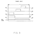
- Operation of the DAC is controlled by a phase logic clocking scheme as seen in Fig. 3 according to which a first voltage supply switch connectivity comprising switches Q 1 , Q 2 are closed by signal phi 1.
- the switch Q 5 is then closed by signal phi 2 to charge capacitor C 1 as noted by V A , which is then stored.
- Switch Q 5 is then opened along with switches Q 1 , Q 2 and the second voltage supply switch connectivity comprising switches Q 3 , Q 4 are closed, phi 1, reversing the power supplies on the string of resistors.
- Switch Q 7 is closed, phi 3, to charge capacitor C 2 as indicated by V B which charge is stored with switch Q 7 being opened.
- Switches Q 6 , Q 8 are then closed, phi 4, to thereby average the voltages on capacitors C 1 , C 2 in the case that C 1 ⁇ C 2 which results in a ratiometric output voltage with enhanced stability.
- capacitor C 3 connected between the non-inverting input of the operational amplifier and voltage supply VSS preferably is chosen to have a smaller value than capacitors C 1 , C 2 allows for voltage drop issues. If the value of a particular resistor in the string which is not between taps n/2 - x and n/2 + x changes it will cause one of V A , V B to increase and, when inversely switched, the other one of V A , V B to decease with the average of the two being stable. This can be shown by the following:
- the DAC made in accordance with the invention has a ratiometric output voltage which is insensitive to the drift of R1, R2 and the DAC resistors.
- the first and second capacitors are of equal value as are the string of resistors; however, resistors of different values can be employed as long as the switching of the taps is symmetrical about the average voltage of the voltages at the supply connectivity switches. Similarly, the capacitors C 1 , C 2 need not be of equal value. Further, resistors may be placed between the connectivity switches and the power supplies.
- DAC's made in accordance with the invention are effective for any potentiometric DAC having adequate span mid supply.
- de-energizing means other than the described techniques can be employed for averaging the potentiometer tap voltages.
- the invention should not be considered as limited to the specific embodiment depicted, but rather as defined in the claims.
Landscapes
- Engineering & Computer Science (AREA)
- Theoretical Computer Science (AREA)
- Analogue/Digital Conversion (AREA)
Abstract
Description


Claims (14)
- A potentiometric digital-to-analogue converter (DAC) including:a plurality of resistors, connected serially in a string, including a plurality of tapping points corresponding to digital input values, a first end and a second end,a network of switches, connected to the ends of the string of resistors, so operable as to effect current flow through the string of resistors in a forward sense in a first configuration of the switches and in a reverse sense in a second configuration of the switches, when the network of switches connects the string of resistors to an electrical energy source,sampling circuit means capable of connection to the tapping points of the string of resistors for sampling and holding first and second voltages available at corresponding tapping points of the string of resistors for, respectively, forward and reverse current flows,voltage-averaging circuit means connected to the sampling circuit means for providing an average of the first and second voltages,a control circuit for controlling the network of switches, the sampling circuit means and the voltage-averaging circuit means, the sampling circuit means, in operation, being connected to tapping points corresponding to digital input values, andan output circuit connected to deliver a signal in response to the output from the voltage-averaging circuit means as an output signal from the digital-to-analogue converter.
- A digital-to-analogue converter as claimed in claim 1, wherein the network of switches includes a first switch connected to the first end of the string of resistors, a second switch connected to the second end of the string of resistors, a third switch connected to the first end of the string of resistors and a fourth switch connected to the second end of the string of resistors, the first and second switches being operable as a pair to effect current flow through the string of resistors in the forward sense and the third and fourth switches operable as a pair to effect current flow through the string of resistors in the reverse sense.
- A digital-to-analogue converter as claimed in claim 1 or claim 2, wherein the sampling circuit means includes fifth and sixth switches capable of connecting the sampling circuit means to selected tapping points of the string of resistors, a first and a second capacitor for storing the first and second voltages and seventh and eighth switches capable of connecting the capacitors together and to the output circuit.
- A digital-to-analogue converter as claimed in claim 1, comprising:a string of n serially connected resistors having first and second end portions,first, second, third and fourth switches and second voltage supplies, the first switch connected to the first voltage supply and the first end portion, the second switch connected to the second voltage supply and the second end portion, the third switch connected to the first end portion and the second voltage supply and the fourth switch connected to the second end portion and the first voltage supply,a first tap connected at a selected location of the string of resistors and a second tap connected to a second location of the string of resistors at an inverse location symmetrical about the average voltage of the voltages at the first and second switches,first and second capacitors and an operational amplifier having a non-inverting and an inverting input and an output,a circuit for connecting the first capacitor to the first tap when the first and second switches are closed and for connecting the second capacitor to the second tap when the third and fourth switches are closed and to average the voltages on the first and second capacitors and input the average of the voltages to the non-inverting input of the operational amplifier anda logic circuit for closing the first and second switches to charge the first capacitor, then to open the first and second switches and close the third and fourth switches to charge the second capacitor.
- A digital-to-analogue converter as claimed in claim 4, further comprising:fifth, sixth, seventh and eighth switches,the first capacitor connected to on a first side to the first tap through the fifth switch and to the non-inverting input through the sixth switch and on a second side to the second voltage supply, the second capacitor connected on a first side to the second tap through the seventh switch and to the non-inverting input through the eighth switch and on a second side to the second voltage supply andthe logic circuit closing the fifth switch along with the first and second switches to charge the first capacitor, then opening the fifth switch along with the first and second switches and closing the seventh switch along with the third and fourth switches to charge the second capacitor, then opening the seventh switch along with the third and fourth switches and closing the sixth and eighth switches to input the average voltage of the first and second capacitors to the non-inverting input of the operational amplifier.
- A digital-to-analogue converter as claimed in claim 4 or claim 5, further comprising a third capacitor connected between the non-inverting input of the operational amplifier and the second power supply.
- A digital-to-analogue converter as claimed in any one of claims 1 to 6, wherein the resistors of the string of serially connected resistors are of like value.
- A digital-to-analogue converter as claimed in claim 1, comprising:a string of n serially connected resistors of like value having first and second end portions,first, second, third and fourth switches and first and second voltage supplies, the first switch connected to the first voltage supply and the first end portion, the second switch connected to the second voltage supply and the second end portion, the third switch connected to the first end portion and the second voltage supply and the fourth switch connected to the second end portion and the first voltage supply,a first tap connected to a selected location of the string of resistors at n/2-x and a second tap connected to a selected location of the string of resistors at n/2+x,first, second and third capacitors and fifth, sixth, seventh and eighth switches and an operational amplifier having a non-inverting and an inverting input and an output,the first capacitor connected on a first side to the first tap through the fifth switch and to the non-inverting input and one side of the third capacitor through the sixth switch and on a second side to the second voltage supply, the other side of the third capacitor connected to the second voltage supply, the second capacitor connected on a first side to the second tap through the seventh switch and to the non-inverting input through the eighth switch and on a second side to the second voltage supply anda logic circuit for closing the first, second and fifth switches to charge the first capacitor, then open the first, second and fifth switches and close the third, fourth and seventh switches to charge the second capacitor, then open the third, fourth and seventh switches and close the sixth and eighth switches to input the average voltage of the first and second capacitors to the non-inverting input of the operational amplifier.
- A digital-to-analogue converter as claimed in any one of claims 2 to 8, wherein the first, second, third and fourth switches are single-pole double-throw switches.
- A digital-to-analogue converter as claimed in any one of claims 2 to 9, wherein the first, second, third and fourth switches include field effect transistors (FETs).
- A method of potentiometric digital-to-analogue conversion including the steps of:providing a plurality of resistors, connected serially in a string, including a plurality of tapping points corresponding to digital input values, a first end and a second end,providing a network of switches, connected to the ends of the string of resistors, so operable as to effect current flow through the string of resistors in a forward sense in a first configuration of the switches and in a reverse sense in a second configuration of the switches, when the network of switches connects the string of resistors to an electrical energy source,providing sampling circuit means capable of connection to the tapping points of the string of resistors for sampling and holding first and second voltages available at corresponding tapping points of the string of resistors for, respectively, forward and reverse current flows,providing voltage-averaging circuit means connected to the sampling circuit means for providing an average of the first and second voltages,providing a control circuit for controlling the network of switches, the sampling circuit means and the voltage-averaging circuit means, the sampling circuit means, in operation, being connected to tapping points corresponding to digital input values,providing an output circuit connected to deliver a signal in response to the output from the voltage-averaging circuit means as an output signal from the digital-to-analogue converter,connecting the string of resistors to an electrical energy source through the network of switches andso operating the control circuit as to provide an output signal from the digital-to-analogue converter.
- A method as claimed in claim 11, comprising the steps of:taking a string of serially connected resistors extending from a first end portion to a second end portion,connecting the first and second end portions to first and second voltage supplies, respectively,taking a first tap at a location of the string of resistors having a fraction of the normal resistance values of the total of the string of resistors from the first to the second end portions, connecting the first tap to a first capacitor to charge the capacitor and storing the charge,disconnecting the first and second end portions from the first and second voltage supplies and connecting the first and second end portions to the second and first voltage supplies, respectively,taking a second tap at a location of the string of resistors having the same selected fraction of the nominal resistance values of the total of the string of resistors from the second to the first end portions, connecting the second tap to a second capacitor to charge the second capacitor and storing the charge andtaking the average voltage to provide a voltage output.
- A method as claimed in claim 12, wherein the resistors of the string are of like value, the first tap being connected to the string of resistors at n/2-x and the second tap being connected to the string of resistors at n/2+x.
- A method as claimed in claim 12 or claim 13, wherein the first and second end portions of the serial resistor string are connected to voltage supplies through series resistors.
Applications Claiming Priority (2)
| Application Number | Priority Date | Filing Date | Title |
|---|---|---|---|
| US09/435,299 US6249239B1 (en) | 1999-11-05 | 1999-11-05 | Potentiometric DAC having improved ratiometric output voltage stability |
| US435299 | 1999-11-05 |
Publications (2)
| Publication Number | Publication Date |
|---|---|
| EP1098441A2 true EP1098441A2 (en) | 2001-05-09 |
| EP1098441A3 EP1098441A3 (en) | 2003-08-27 |
Family
ID=23727826
Family Applications (1)
| Application Number | Title | Priority Date | Filing Date |
|---|---|---|---|
| EP00309743A Withdrawn EP1098441A3 (en) | 1999-11-05 | 2000-11-03 | Potentiometric DAC having improved ratiometric output voltage stability |
Country Status (3)
| Country | Link |
|---|---|
| US (1) | US6249239B1 (en) |
| EP (1) | EP1098441A3 (en) |
| JP (1) | JP4497705B2 (en) |
Families Citing this family (4)
| Publication number | Priority date | Publication date | Assignee | Title |
|---|---|---|---|---|
| JP4397291B2 (en) * | 2004-06-29 | 2010-01-13 | Okiセミコンダクタ株式会社 | Display device drive circuit and display device drive method |
| KR100708939B1 (en) * | 2005-08-08 | 2007-04-17 | 삼성전기주식회사 | Digital / Analog Converter |
| WO2010079530A1 (en) * | 2009-01-07 | 2010-07-15 | 株式会社アドバンテスト | Circuit and method for digital-analog conversion |
| US10840941B1 (en) * | 2020-01-06 | 2020-11-17 | Nxp B.V. | System and method for improving matching in a signal converter |
Family Cites Families (8)
| Publication number | Priority date | Publication date | Assignee | Title |
|---|---|---|---|---|
| US4338591A (en) * | 1981-06-09 | 1982-07-06 | Analog Devices, Incorporated | High resolution digital-to-analog converter |
| JPS5944125A (en) * | 1982-09-07 | 1984-03-12 | Toshiba Corp | Digital-analog converter |
| JPS60199214A (en) * | 1984-03-23 | 1985-10-08 | Toshiba Corp | Voltage dividing circuit |
| JPS6126330A (en) * | 1984-07-16 | 1986-02-05 | Toshiba Corp | Resistance type potential dividing circuit |
| JP2675706B2 (en) * | 1992-01-29 | 1997-11-12 | 株式会社東芝 | Resistor string circuit |
| US5617091A (en) * | 1994-09-02 | 1997-04-01 | Lowe, Price, Leblanc & Becker | Resistance ladder, D-A converter, and A-D converter |
| US6163289A (en) * | 1997-09-23 | 2000-12-19 | Philips Electronics North America Corp. | Differential voltage digital-to-analog converter |
| JPH11145835A (en) * | 1997-11-06 | 1999-05-28 | Kawasaki Steel Corp | Ladder resistance |
-
1999
- 1999-11-05 US US09/435,299 patent/US6249239B1/en not_active Expired - Fee Related
-
2000
- 2000-11-02 JP JP2000335295A patent/JP4497705B2/en not_active Expired - Fee Related
- 2000-11-03 EP EP00309743A patent/EP1098441A3/en not_active Withdrawn
Also Published As
| Publication number | Publication date |
|---|---|
| US6249239B1 (en) | 2001-06-19 |
| JP2001168718A (en) | 2001-06-22 |
| JP4497705B2 (en) | 2010-07-07 |
| EP1098441A3 (en) | 2003-08-27 |
Similar Documents
| Publication | Publication Date | Title |
|---|---|---|
| US6414616B1 (en) | Architecture for voltage scaling DAC | |
| US7167121B2 (en) | Method and apparatus for split reference sampling | |
| US5495245A (en) | Digital-to-analog converter with segmented resistor string | |
| US7616144B2 (en) | Resistor ladder interpolation for PGA and DAC | |
| US7884747B2 (en) | Digital to analog converters having circuit architectures to overcome switch losses | |
| US6466149B2 (en) | Apparatus and method for digital to analog conversion | |
| JP2001244816A (en) | Digitally switched potentiometer with improved linearity and settling time | |
| JP2006517765A (en) | Automatic zeroing in critical continuous time applications | |
| JPH0566774B2 (en) | ||
| JPS59132231A (en) | Analog-digital converter | |
| US20030117307A1 (en) | Resistor string dac with current source lsbs | |
| EP0661817B1 (en) | Digital-to-analog converter | |
| US6885328B1 (en) | Digitally-switched impedance with multiple-stage segmented string architecture | |
| JP3857450B2 (en) | Successive comparison type analog-digital conversion circuit | |
| US5731775A (en) | Subranging converter with plurality of resistor strings and transistor switches | |
| US5055847A (en) | Differential sensing current-steering analog-to-digital converter | |
| US5248974A (en) | Dielectric relaxation correction circuit for charge-redistribution a/d converters | |
| US6975261B1 (en) | High accuracy digital to analog converter using parallel P and N type resistor ladders | |
| US6008749A (en) | Mask programmable low power voltage/current-mode ADC | |
| US4837572A (en) | Digital-to-analog converter | |
| US5612696A (en) | Digital-to-analog converter of current segmentation | |
| KR20010016922A (en) | Digital-to-analog converter capable of fast switching and precision voltage conversion | |
| EP2853032A1 (en) | Digital-to-analog-converter with resistor ladder | |
| US6249239B1 (en) | Potentiometric DAC having improved ratiometric output voltage stability | |
| JPS625377B2 (en) |
Legal Events
| Date | Code | Title | Description |
|---|---|---|---|
| PUAI | Public reference made under article 153(3) epc to a published international application that has entered the european phase |
Free format text: ORIGINAL CODE: 0009012 |
|
| AK | Designated contracting states |
Kind code of ref document: A2 Designated state(s): AT BE CH CY DE DK ES FI FR GB GR IE IT LI LU MC NL PT SE TR |
|
| AX | Request for extension of the european patent |
Free format text: AL;LT;LV;MK;RO;SI |
|
| PUAL | Search report despatched |
Free format text: ORIGINAL CODE: 0009013 |
|
| AK | Designated contracting states |
Designated state(s): AT BE CH CY DE DK ES FI FR GB GR IE IT LI LU MC NL PT SE TR |
|
| AX | Request for extension of the european patent |
Extension state: AL LT LV MK RO SI |
|
| 17P | Request for examination filed |
Effective date: 20040205 |
|
| AKX | Designation fees paid |
Designated state(s): DE FR GB |
|
| 17Q | First examination report despatched |
Effective date: 20050214 |
|
| STAA | Information on the status of an ep patent application or granted ep patent |
Free format text: STATUS: THE APPLICATION IS DEEMED TO BE WITHDRAWN |
|
| 18D | Application deemed to be withdrawn |
Effective date: 20050625 |