EP1098384A2 - Dielectric filter, dielectric duplexer, and communication apparatus - Google Patents
Dielectric filter, dielectric duplexer, and communication apparatus Download PDFInfo
- Publication number
- EP1098384A2 EP1098384A2 EP00122902A EP00122902A EP1098384A2 EP 1098384 A2 EP1098384 A2 EP 1098384A2 EP 00122902 A EP00122902 A EP 00122902A EP 00122902 A EP00122902 A EP 00122902A EP 1098384 A2 EP1098384 A2 EP 1098384A2
- Authority
- EP
- European Patent Office
- Prior art keywords
- dielectric
- resonators
- duplexer
- coupled
- filter
- Prior art date
- Legal status (The legal status is an assumption and is not a legal conclusion. Google has not performed a legal analysis and makes no representation as to the accuracy of the status listed.)
- Granted
Links
- 238000004891 communication Methods 0.000 title claims abstract description 11
- 239000004020 conductor Substances 0.000 claims abstract description 36
- 230000005540 biological transmission Effects 0.000 claims description 9
- 239000003989 dielectric material Substances 0.000 claims description 5
- 239000000758 substrate Substances 0.000 description 11
- 238000010586 diagram Methods 0.000 description 8
- 238000010276 construction Methods 0.000 description 5
- 230000008878 coupling Effects 0.000 description 5
- 238000010168 coupling process Methods 0.000 description 5
- 238000005859 coupling reaction Methods 0.000 description 5
- UUDAMDVQRQNNHZ-UHFFFAOYSA-N (S)-AMPA Chemical compound CC=1ONC(=O)C=1CC(N)C(O)=O UUDAMDVQRQNNHZ-UHFFFAOYSA-N 0.000 description 3
- 238000004519 manufacturing process Methods 0.000 description 3
- 239000003990 capacitor Substances 0.000 description 1
- 238000003780 insertion Methods 0.000 description 1
- 230000037431 insertion Effects 0.000 description 1
- 238000012986 modification Methods 0.000 description 1
- 230000004048 modification Effects 0.000 description 1
- 238000003199 nucleic acid amplification method Methods 0.000 description 1
- 230000002093 peripheral effect Effects 0.000 description 1
Images



Classifications
-
- H—ELECTRICITY
- H01—ELECTRIC ELEMENTS
- H01P—WAVEGUIDES; RESONATORS, LINES, OR OTHER DEVICES OF THE WAVEGUIDE TYPE
- H01P1/00—Auxiliary devices
- H01P1/20—Frequency-selective devices, e.g. filters
- H01P1/201—Filters for transverse electromagnetic waves
- H01P1/202—Coaxial filters
-
- H—ELECTRICITY
- H01—ELECTRIC ELEMENTS
- H01P—WAVEGUIDES; RESONATORS, LINES, OR OTHER DEVICES OF THE WAVEGUIDE TYPE
- H01P1/00—Auxiliary devices
- H01P1/20—Frequency-selective devices, e.g. filters
- H01P1/201—Filters for transverse electromagnetic waves
- H01P1/205—Comb or interdigital filters; Cascaded coaxial cavities
- H01P1/2056—Comb filters or interdigital filters with metallised resonator holes in a dielectric block
Definitions
- the present invention relates to a dielectric filter for use in microwave bands and the like, a dielectric duplexer, and a communication apparatus using them.
- Conventional filters for use in microwave bands and the like include a dielectric filter that is formed by providing an inner-conductor-forming opening or inner-conductor-forming openings in a dielectric block to form one resonator or a plurality of resonators, and by providing an outer conductor on outer faces of the dielectric block.
- terminal electrodes coupled by electrostatic capacitance to the inner conductors are provided to perform unbalanced-type input and/or output of signals. Therefore, to feed signals to, for example, a balanced-input/output-type amplifier circuit, a balun (balanced-unbalanced converter) is needed to convert unbalanced-type signals to balanced-type signals.
- a balun balanced-unbalanced converter
- the dielectric filter of this type gives rise to problems. Insertion loss because of the balun is large. Also, spacing must be secured for arranging the balun on a circuit substrate, and miniaturization cannot therefore be implemented.
- Japanese Unexamined Patent Application Publication No. 7-254807 discloses a dielectric filter capable of performing balanced-type input and/or output of signals.
- this balanced-type dielectric filter to electrically connect an inner conductor to terminal electrodes on an outer face of a dielectric block, openings must be formed perpendicular to an inner-conductor-forming opening. It is very difficult to form the openings perpendicular to the inner-conductor-forming opening in the dielectric block. Therefore, manufacturing costs are increased.
- both balancing characteristics and the degree of external coupling are influenced by the positions of the openings that form the aforementioned connecting conductors, high forming accuracy is required to obtain predetermined characteristics. Also, adjustment after forming is difficult.
- the present invention provides a dielectric filter, a dielectric duplexer, and a communication apparatus using them, which allow balanced-type input and/or output of signals to be implemented, and concurrently, allow manufacturing costs to be easily reduced.
- a dielectric filter is made by forming a conductor film on a single dielectric material to provide at least two ⁇ /2 resonators that individually have two ends being open-circuited, that resonate at 1 ⁇ 2-wavelength at a predetermined frequency, and that are coupled. Terminals are individually coupled by electrostatic capacitance to vicinities of the two open-circuit ends of each of the ⁇ /2 resonators and are used for balanced input and/or output of signals.
- each of the two ⁇ /2 resonators may either be formed using a microstrip line or a strip line, or be formed of a dielectric coaxial resonator made by providing the conductor films in and on a dielectric block.
- no balun needs to be formed, and a filter for performing balanced input and/or input of signals can be easily formed on a dielectric substrate.
- each of the two ⁇ /2 resonators may be formed of a dielectric coaxial resonator made by providing the conductor films in and on a dielectric block.
- the dielectric filter being formed of the coaxial resonators, mounting of only the dielectric filter on a mounting substrate or the like allows a circuit for performing balanced input and/or output of signals and a circuit having the filter to be concurrently formed. Therefore, the area occupied on the mounting substrate can be reduced, and the mounting efficiency can be improved.
- a dielectric duplexer is formed by providing a transmission filter and a reception filter that have the above-described configuration.
- the dielectric duplexer can be used as an antenna-sharing unit that performs balanced input and/or output of transmission signals and/or reception signals.
- miniaturization can be implemented for amplifier circuits and the like that perform balanced input and/or output as well as a high-frequency circuit section in the vicinity of the antenna.
- a communication apparatus is formed by using one of the above-described dielectric filters and/or the above-described dielectric duplexer. Therefore, a small and light communication apparatus can be constructed.
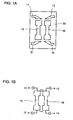
- FIGS. 1A and 1B a description will be given of a configuration of a dielectric filter according to a first embodiment of the present invention.
- FIG. 1A is a plan view of the dielectric filter.
- the individual reference symbols 15 and 16 denote strip line electrodes; 11, 12, 13, and 14 denote terminal electrodes. These electrodes are formed on an upper face of a dielectric substrate 20.
- a ground electrode is formed on substantially the entirety of a lower face of the dielectric substrate 20.
- the dielectric substrate 20, the strip line electrodes 15 and 16, and the ground electrode form individual microstrip-line resonators. Electrostatic capacitance is generated between each of the terminal electrodes 11 and 12 and the vicinity of corresponding ends of the strip line electrode 15. Similarly, electrostatic capacitance is generated in between each of the terminal electrodes 13 and 14 and the vicinity of corresponding ends of the strip line electrode 16.
- the aforementioned microstrip-line resonators comprising the strip line electrodes 15 and 16 work as two-end-open-circuited ⁇ /2 resonators.
- the centers of the strip line electrodes 15 and 16 are equivalent to short-circuit points.
- the widths of the strip line electrodes at the short-circuit points are reduced, and the widths thereof at the open-circuit ends are increased.
- the two resonators with the strip line electrodes 15 and 16 are permitted to couple together by electrostatic capacitance.
- the line length required to obtain a predetermined resonant frequency is reduced, to obtain overall miniaturization.
- FIG. 1B is an equivalent circuit diagram of the dielectric filter shown in FIG. 1A.
- the two resonators having the strip line electrodes 15 and 16 are coupled together by capacitance, and the terminal electrodes 11 to 14 and the two resonators are also coupled by capacitance to each other.
- the potentials of the two ends of each of the resonators have the relationship of a 180-degree phase difference. Therefore, the terminal electrodes 11 and 12 and the terminal electrodes 13 and 14 can individually serve as balanced input/output terminals.
- the terminal electrodes 11 and 12 can be used as balanced input terminals
- the terminal electrodes 13 and 14 can be used as balanced output terminals.
- the dielectric filter can be used as a two-stage bandpass filter.
- the external coupling between the resonators and the terminal electrodes is by electrostatic capacitance. Therefore, the external coupling can be easily adjusted by adjusting the distances and the areas between the resonators and the terminal electrodes.
- an external terminal is formed in the vicinity of each end of each resonator, symmetry of the electrode patterns can be improved, and stabilized balancing characteristics can thereby be obtained.
- resonators are coupled by capacitance, they may also be coupled by using lumped-parameter elements such as capacitors and inductors.
- resonators made of strip lines may be formed by providing the individual electrode patterns shown in FIGS. 1A and 1B on two dielectric substrates.
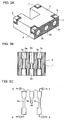
- FIGS. 2A and 2B a description will be given of a configuration of a dielectric filter according to a second embodiment.
- FIG. 2A is a perspective view of the dielectric filter
- FIG. 2B is a cross-sectional view taken in a plane extending through the central axes of inner-conductor-forming openings 2a and 2b that are shown in FIG. 2A.
- the upper face in the state shown in FIG. 2A is a mounting face for mounting on a substrate.
- 1 denotes a dielectric block that is substantially rectangular parallelepiped, and the two inner-conductor-forming openings 2a and 2b are provided therein.
- An outer conductor 3 is provided on four peripheral faces, excluding the faces at the end portions of the inner-conductor-forming openings 2a and 2b (four faces). Terminal electrodes 5, 6, 7, and 8 are individually formed to be isolated from the outer conductor 3.
- Inner conductors 4a and 4b are provided on inner faces of the inner-conductor-forming openings 2a and 2b.
- the inner conductors 4a and 4b individually work as ⁇ /2 resonators that resonate at a half wavelength and that have two ends being open-circuited.
- the terminal electrodes 5 and 6 are individually coupled by capacitance to the vicinities of open-circuit ends of the inner conductor 4a on the inner surface of the inner-conductor-forming opening 2a.
- the terminal electrodes 7 and 8 are individually coupled by capacitance to the vicinities of open-circuit ends of the inner conductor 4b on the inner surface of the inner-conductor-forming opening 2b.
- FIGS. 2A and 2B An equivalent circuit diagram of the dielectric filter shown in FIGS. 2A and 2B is similar to that shown in FIG. 1B.
- the dielectric filter described above is used as a balanced-input/output-type dielectric filter that has characteristics of a two-stage bandpass filter.
- the external coupling between the resonators and the terminal electrodes is made by electrostatic capacitance. Therefore, the external coupling can be easily adjusted by adjusting distances and areas between the resonators and the terminal electrodes.
- two pairs of the terminal electrodes, each performing balanced input and/or output are formed in positions symmetrical both in the direction between the two open-circuited end faces and in the direction between the input and the output of signals. This allows stabilized balancing characteristics to be obtained.
- FIGS. 3A to 3C a description will be given of a configuration of a dielectric filter according to a third embodiment.
- FIG. 3A is a perspective view of the dielectric filter.
- FIG. 3B is a cross-sectional view taken in a plane extending through the central axes of inner-conductor-forming openings 2a, 2b, and 2c that are shown in FIG. 3A.
- FIG. 3C is a circuit diagram of the dielectric filter shown in FIGS. 3A and 3B.
- the upper face in the state shown in FIG. 3A is a mounting face for mounting on a substrate.
- 1 denotes a dielectric block that is substantially a rectangular parallelepiped and the three inner-conductor-forming openings 2a, 2b, and 2c are provided therein.
- the inner-conductor-forming opening 2b is arranged to be substantially half the length of each of the inner-conductor-forming openings 2a and 2c, one end thereof is arranged to be an open-circuited end face, and the other end is arranged to be a short-circuit-end face. Opening end portions of the inner-conductor-forming openings 2a and 2c are arranged to be open-circuited end faces.
- An outer conductor 3 is formed on all the outer faces except these open-circuited end faces, and terminal electrodes 5, 6, 7, and 8 are formed so as to be isolated from the outer conductor 3.
- Inner conductors 4a, 4b, and 4c are formed on inner faces of the inner-conductor-forming openings 2a, 2b and 2c, respectively.
- the inner conductors 4a and 4c individually work as ⁇ /2 resonators that resonate at a half wavelength and have two ends open-circuited.
- the inner conductor 4b works as a ⁇ /4 resonator that resonates at 1/4 wavelength and has one end open-circuited and the other end short-circuited.
- the adjacent resonators are coupled together by capacitance.
- the terminal electrodes 5 and 6 are individually coupled by capacitance to the vicinities of the open-circuit ends of the inner conductors 4a on the inner surface of the inner-conductor-forming opening 2a.
- the terminal electrodes 7 and 8 are individually coupled by capacitance to the vicinities of the open-circuit ends of the inner conductor 4c on the inner surface of the inner-conductor-forming opening 2c.
- the outer resonators are arranged to be ⁇ /2 resonators, and the inner resonator is arranged to be a ⁇ /4 resonator.
- the arrangement may be such that, conversely, outer resonators are ⁇ /4 resonators, and an inner resonator is a ⁇ /2 resonator.
- the number of the resonators may be four or more.
- the arrangement of at least one of the plurality of resonators to be the ⁇ /4 resonator produces an advantage in that the frequency that generates spurious-mode components can be adjusted. Furthermore, it produces an advantage that the spurious-mode frequency can be adjusted to a level (value) that causes no influence on the characteristics of the dielectric filter.
- FIGS. 4A to 4C a description will be given of a configuration of a dielectric duplexer according to a fourth embodiment.
- FIG. 4A is a perspective view of the dielectric duplexer.
- FIG. 4B is a cross-sectional view taken in a plane extending through the central axes of individual inner-conductor-forming openings 2a to 2e in the dielectric duplexer.
- FIG. 4C is a circuit diagram of the dielectric duplexer.
- the upper face in the state shown in FIG. 4A is a mounting face for mounting on a substrate.
- 1 denotes a dielectric block that is substantially a rectangular parallelepiped, and the five inner-conductor-forming openings 2a to 2e are provided therein.
- Two end faces of the inner-conductor-forming openings 2a to 2e are arranged to be open-circuited end faces.
- An outer conductor 3 is formed on the four outer faces excluding the open-circuited end faces.
- Terminal electrodes 5 to 10 are formed on the dielectric block and isolated from the outer conductor 3.
- Inner conductors 4a to 4e are formed on inner faces of the inner-conductor-forming openings 2a to 2e, respectively.
- a dielectric filter is configured with two resonators similar to those shown in FIGS. 2A and 2B corresponding to the inner-conductor-forming openings 2a and 2b, and another dielectric filter has three resonators corresponding to the inner-conductor-forming openings 2c, 2d, and 2e.
- the terminal electrodes 5 and 6 are coupled by capacitance to the vicinity of open-circuited ends of an inner conductor 4a provided on an inner surface of the inner-conductor-forming opening 2a.
- the terminal electrodes 9 and 10 are coupled by capacitance to the vicinity of open-circuited ends of an inner conductor 4e provided on an inner surface of the inner-conductor-forming opening 2e.
- the terminal electrodes 7 and 8 are coupled by capacitance to the vicinity of both open-circuited ends of an inner conductor 4b provided on an inner surface of the inner-conductor-forming opening 2b, and open-circuited ends of an inner conductor 4c provided on an inner surface of the inner conductor 2c.
- the described dielectric duplexer can be used as an antenna-sharing unit that uses the terminal electrodes 5 and 6 as a transmission-signal input port, the terminal electrodes 7 and 8 as an antenna port, and the terminal electrodes 9 and 10 as a reception-signal output port.
- ANT denotes a transmission/reception antenna
- DPX denotes a duplexer
- BPFa, BPFb, and BPFc each denote a bandpass filter
- AMPa and AMPb each denote an amplifier circuit
- MIXa and MIXb each denote a mixer
- OSC denotes an oscillator
- DIV denotes a synthesizer.
- the mixer MIXa uses modulation signals to modulate frequency signals outputted from the synthesizer DIV.
- the bandpass filter BPFa passes the signals only in a transmission-signal band.
- the amplifier circuit AMPa performs power-amplification of the signals, and transmits them via the antenna ANT via the duplexer DPX.
- the bypass filter BPFb passes only signals in a reception-signal band out of those outputted from the duplexer DPX, and the amplifier circuit AMPb amplifies them.
- the mixer MIXb mixes individual frequency signals outputted from the bandpass filter BPFc and reception signals and output mixed signals to intermediate frequency signals IF.
- amplifier circuits AMPa and AMPb shown in FIG. 5 are balanced-input/output-type circuits
- a duplexer having the construction as shown in FIG. 4 is used for the portion of the duplexer DPX.
- bandpass filters BPFa and BPFb dielectric filters of the constructions as shown in FIGS. 1 to 3 are used. In this way, with these balanced-type circuits, since signals can be filtered, and concurrently, can be inputted and/or outputted without a balun being used, a communication apparatus that is small in overall size can be constructed.
Landscapes
- Physics & Mathematics (AREA)
- Electromagnetism (AREA)
- Control Of Motors That Do Not Use Commutators (AREA)
Abstract
Description
Claims (14)
- A balanced dielectric filter comprising conductor films (3) formed on dielectric material (1), said filter comprising:at least two coupled λ/2 resonators (15,16;4a,4b;4a,4c), each having two open-circuited ends, and having ½-wavelength resonance at a predetermined frequency; anda pair of terminals (11,12,13,14;5,6,7,8)each being coupled respectively to the vicinity of a respective one of said open-circuited ends of a corresponding one of said λ/2 resonators (15,16;4a,4b;4a,4c) and operable to perform balanced input and/or output of signals.
- A dielectric filter as claimed in claim 1, wherein said terminals (11,12,13,14;5,6,7,8) are coupled to said resonators (15,16;4a,4b;4a,4c) by electrostatic capacitance.
- A dielectric filter as claimed in claim 1 or 2, wherein each of said at least two λ/2 resonators (15,16) comprises one of a microstrip line and a strip line.
- A dielectric filter as claimed in claim 1 or 2, wherein each of said at least two λ/2 resonators (4a,4b;4a,4c) is a dielectric coaxial resonator.
- A dielectric filter as claimed in claim 1 or 2, further comprising an intermediate resonator (4b) coupled to both of said at least two coupled λ/2 resonators (4a,4c).
- A dielectric filter as claimed in claim 5, wherein said intermediate resonator (4b) is a λ/4 resonator.
- A dielectric duplexer comprising a pair of balanced dielectric filters comprising conductor films (3) formed on dielectric material (1), each said filter comprising:at least first (4a,4c) and second (4b,4e) coupled λ/2 resonators, each having two open-circuited ends, and having ½-wavelength resonance at a predetermined frequency; andfirst (5,6,9,10) and second (7,8) pairs of terminals each being coupled respectively to the vicinity of a respective one of said open-circuited ends of a corresponding one of said first (4a,4c) and second (4b,4e) λ/2 resonators and operable to perform balanced input and/or output of signals;said first pair (5,6) of terminals of said first resonator (4a) providing a transmission input of said duplexer, said first pair (9,10) of terminals of said second resonator (4e) providing a reception output of said duplexer, and said second pairs (7,8) of terminals being connected to an antenna terminal of said duplexer.
- A dielectric duplexer as claimed in claim 7, wherein said terminals (5,6,7,8,9,10) are coupled to said resonators (4a,4b,4c,4e) by electrostatic capacitance.
- A dielectric duplexer as claimed in claim 7 or 8, wherein each of said at least two λ/2 resonators comprises one of a microstrip line and a strip line.
- A dielectric duplexer as claimed in claim 7, wherein each of said at least two λ/2 resonators is a dielectric coaxial resonator (4a,4b,4c,4e).
- A dielectric duplexer as claimed in one of claims7 to 10, further comprising an intermediate resonator (4d) coupled to both of said at least two coupled λ/2 resonators (4c,4e).
- A dielectric duplexer as claimed in claim 11, wherein said intermediate resonator (4d) is a λ/4 resonator.
- A communication apparatus comprising:a balanced high-frequency circuit comprising one of a transmission circuit and a reception circuit; andconnected to said balanced high-frequency circuit, a balanced dielectric filter comprising conductor films (3) formed on dielectric material (1), said filter comprising:at least two coupled λ/2 resonators (4a,4b;4a,4c), each having two open-circuited ends, and having ½-wavelength resonance at a predetermined frequency; anda pair of terminals (5,6,7,8) each being coupled respectively to the vicinity of a respective one of said open-circuited ends of a corresponding one of said λ/2 resonators (4a,4b;4a,4c) and operable to perform balanced input and/or output of signals.
- A communication apparatus comprising:a transmission circuit;a reception circuit; anda dielectric duplexer comprising a pair of balanced dielectric filters comprising conductor films (3) formed on dielectric material (1), each said filter comprising:at least first (4a,4c) and second (4b,4e) coupled λ/2 resonators, each having two open-circuited ends, and having ½-wavelength resonance at a predetermined frequency; andfirst (5,6,9,10) and second (7,8) pairs of terminals each being coupled respectively to the vicinity of a respective one of said open-circuited ends of a corresponding one of said first (4a,4c) and second (4b,4e) λ/2 resonators and operable to perform balanced input and/or output of signals;said first pair (5,6) of terminals of said first resonator (4a) providing a transmission input of said duplexer, said first pair (9,10) of terminals of said second resonator (4e) providing a reception output of said duplexer, and said second pairs (7,8) of terminals being connected to an antenna terminal of said duplexer;said transmission circuit being connected to said transmission input of said duplexer, and said reception circuit being connected to said reception output of said duplexer.
Applications Claiming Priority (2)
| Application Number | Priority Date | Filing Date | Title |
|---|---|---|---|
| JP31465799 | 1999-11-05 | ||
| JP31465799A JP2001136003A (en) | 1999-11-05 | 1999-11-05 | Dielectric filter, dielectric duplexer and communication unit |
Publications (3)
| Publication Number | Publication Date |
|---|---|
| EP1098384A2 true EP1098384A2 (en) | 2001-05-09 |
| EP1098384A3 EP1098384A3 (en) | 2002-05-15 |
| EP1098384B1 EP1098384B1 (en) | 2009-04-22 |
Family
ID=18055977
Family Applications (1)
| Application Number | Title | Priority Date | Filing Date |
|---|---|---|---|
| EP00122902A Expired - Lifetime EP1098384B1 (en) | 1999-11-05 | 2000-10-20 | Dielectric filter, dielectric duplexer, and communication apparatus |
Country Status (6)
| Country | Link |
|---|---|
| US (1) | US6535079B1 (en) |
| EP (1) | EP1098384B1 (en) |
| JP (1) | JP2001136003A (en) |
| KR (1) | KR100352573B1 (en) |
| CN (1) | CN1177388C (en) |
| DE (1) | DE60042051D1 (en) |
Cited By (2)
| Publication number | Priority date | Publication date | Assignee | Title |
|---|---|---|---|---|
| EP1294042A3 (en) * | 2001-09-14 | 2003-11-19 | Murata Manufacturing Co., Ltd. | Dielectric filter, dielectric duplexer, and communication device |
| GB2389239A (en) * | 2002-03-29 | 2003-12-03 | Ngk Spark Plug Co | Dielectric filter |
Families Citing this family (5)
| Publication number | Priority date | Publication date | Assignee | Title |
|---|---|---|---|---|
| JP3636122B2 (en) | 2001-09-19 | 2005-04-06 | 株式会社村田製作所 | Dielectric filter, dielectric duplexer, and communication device |
| JP5788452B2 (en) * | 2013-09-13 | 2015-09-30 | 東光株式会社 | Dielectric waveguide resonator and dielectric waveguide filter using the same |
| EP3118928A1 (en) * | 2015-07-17 | 2017-01-18 | Toko, Inc. | Input/output coupling structure of dielectric waveguide |
| WO2020087378A1 (en) * | 2018-10-31 | 2020-05-07 | 华为技术有限公司 | Dielectric filter and communication device |
| CN114374069B (en) * | 2021-12-31 | 2024-10-01 | 天津大学 | Frequency hopping filter using dielectric coaxial resonator |
Family Cites Families (6)
| Publication number | Priority date | Publication date | Assignee | Title |
|---|---|---|---|---|
| BE533239A (en) * | 1952-05-08 | |||
| US3735289A (en) * | 1971-11-26 | 1973-05-22 | Collins Radio Comp | Transmitter combiner having coupled tuned circuits |
| US4371853A (en) * | 1979-10-30 | 1983-02-01 | Matsushita Electric Industrial Company, Limited | Strip-line resonator and a band pass filter having the same |
| JP3117598B2 (en) * | 1994-03-15 | 2000-12-18 | アルプス電気株式会社 | Balanced dielectric filter and high frequency circuit using balanced dielectric filter |
| US5825263A (en) * | 1996-10-11 | 1998-10-20 | Northern Telecom Limited | Low radiation balanced microstrip bandpass filter |
| US6222431B1 (en) * | 1998-02-27 | 2001-04-24 | Matsushita Electric Industrial Co., Ltd. | Balanced dielectric filter |
-
1999
- 1999-11-05 JP JP31465799A patent/JP2001136003A/en active Pending
-
2000
- 2000-10-20 EP EP00122902A patent/EP1098384B1/en not_active Expired - Lifetime
- 2000-10-20 DE DE60042051T patent/DE60042051D1/en not_active Expired - Fee Related
- 2000-11-03 KR KR1020000065224A patent/KR100352573B1/en not_active Expired - Lifetime
- 2000-11-06 CN CNB001328352A patent/CN1177388C/en not_active Expired - Lifetime
- 2000-11-06 US US09/707,683 patent/US6535079B1/en not_active Expired - Lifetime
Cited By (4)
| Publication number | Priority date | Publication date | Assignee | Title |
|---|---|---|---|---|
| EP1294042A3 (en) * | 2001-09-14 | 2003-11-19 | Murata Manufacturing Co., Ltd. | Dielectric filter, dielectric duplexer, and communication device |
| US6771149B2 (en) | 2001-09-14 | 2004-08-03 | Murata Manufacturing Co., Ltd. | Dielectric filter, dielectric duplexer, and communication device |
| GB2389239A (en) * | 2002-03-29 | 2003-12-03 | Ngk Spark Plug Co | Dielectric filter |
| US6844796B2 (en) | 2002-03-29 | 2005-01-18 | Ngk Spark Plug Co., Ltd. | Dielectric filter having increased bandwidth |
Also Published As
| Publication number | Publication date |
|---|---|
| EP1098384A3 (en) | 2002-05-15 |
| US6535079B1 (en) | 2003-03-18 |
| CN1296306A (en) | 2001-05-23 |
| CN1177388C (en) | 2004-11-24 |
| EP1098384B1 (en) | 2009-04-22 |
| JP2001136003A (en) | 2001-05-18 |
| KR100352573B1 (en) | 2002-09-12 |
| DE60042051D1 (en) | 2009-06-04 |
| KR20010051433A (en) | 2001-06-25 |
Similar Documents
| Publication | Publication Date | Title |
|---|---|---|
| JP3642276B2 (en) | Antenna device and communication device | |
| US6535077B1 (en) | Dielectric filter, dielectric duplexer, and communication apparatus | |
| US6236288B1 (en) | Dielectric filter having at least one stepped resonator hole with a recessed or protruding portion, the stepped resonator hole extending from a mounting surface | |
| US6304158B1 (en) | Dielectric filter, composite dielectric filter, antenna duplexer, and communication apparatus | |
| US6281768B1 (en) | Dielectric filter, duplexer, and communication apparatus | |
| US6420942B1 (en) | Dielectric filter, dielectric duplexer, and communication apparatus | |
| US6549093B2 (en) | Dielectric filter, duplexer, and communication apparatus incorporating the same | |
| US6535079B1 (en) | Dielectric filter, dielectric duplexer, and communication apparatus | |
| US6833773B1 (en) | Dielectric filter, dielectric duplexer, and communication apparatus incorporating the same | |
| US6771149B2 (en) | Dielectric filter, dielectric duplexer, and communication device | |
| KR100519014B1 (en) | Dielectric filter, dielectric duplexer and communication apparatus | |
| US6788167B2 (en) | Dielectric filter, dielectric duplexer, and communication apparatus incorporating the same | |
| KR20010006929A (en) | Dielectric Filter, Dielectric Duplexer, and Communication Apparatus |
Legal Events
| Date | Code | Title | Description |
|---|---|---|---|
| PUAI | Public reference made under article 153(3) epc to a published international application that has entered the european phase |
Free format text: ORIGINAL CODE: 0009012 |
|
| 17P | Request for examination filed |
Effective date: 20001020 |
|
| AK | Designated contracting states |
Kind code of ref document: A2 Designated state(s): AT BE CH CY DE DK ES FI FR GB GR IE IT LI LU MC NL PT SE |
|
| AX | Request for extension of the european patent |
Free format text: AL;LT;LV;MK;RO;SI |
|
| PUAL | Search report despatched |
Free format text: ORIGINAL CODE: 0009013 |
|
| AK | Designated contracting states |
Kind code of ref document: A3 Designated state(s): AT BE CH CY DE DK ES FI FR GB GR IE IT LI LU MC NL PT SE |
|
| AX | Request for extension of the european patent |
Free format text: AL;LT;LV;MK;RO;SI |
|
| RIC1 | Information provided on ipc code assigned before grant |
Free format text: 7H 01P 1/205 A, 7H 01P 1/203 B, 7H 01P 1/213 B |
|
| AKX | Designation fees paid |
Designated state(s): DE FR GB |
|
| RAP1 | Party data changed (applicant data changed or rights of an application transferred) |
Owner name: MURATA MANUFACTURING CO., LTD. |
|
| GRAP | Despatch of communication of intention to grant a patent |
Free format text: ORIGINAL CODE: EPIDOSNIGR1 |
|
| RIN1 | Information on inventor provided before grant (corrected) |
Inventor name: NISHIJIMA, SHOHACHI,C/O (A170) IP DEPARTMENT Inventor name: HIROSHIMA, MOTOHARU,C/O (A170) IP DEPARTMENT Inventor name: KATO, HIDEYUKI,C/O (A170) IP DEPARTMENT |
|
| GRAS | Grant fee paid |
Free format text: ORIGINAL CODE: EPIDOSNIGR3 |
|
| GRAA | (expected) grant |
Free format text: ORIGINAL CODE: 0009210 |
|
| AK | Designated contracting states |
Kind code of ref document: B1 Designated state(s): DE FR GB |
|
| REG | Reference to a national code |
Ref country code: GB Ref legal event code: FG4D |
|
| REF | Corresponds to: |
Ref document number: 60042051 Country of ref document: DE Date of ref document: 20090604 Kind code of ref document: P |
|
| PLBE | No opposition filed within time limit |
Free format text: ORIGINAL CODE: 0009261 |
|
| STAA | Information on the status of an ep patent application or granted ep patent |
Free format text: STATUS: NO OPPOSITION FILED WITHIN TIME LIMIT |
|
| 26N | No opposition filed |
Effective date: 20100125 |
|
| REG | Reference to a national code |
Ref country code: FR Ref legal event code: ST Effective date: 20100630 |
|
| PG25 | Lapsed in a contracting state [announced via postgrant information from national office to epo] |
Ref country code: DE Free format text: LAPSE BECAUSE OF NON-PAYMENT OF DUE FEES Effective date: 20100501 Ref country code: FR Free format text: LAPSE BECAUSE OF NON-PAYMENT OF DUE FEES Effective date: 20091102 |
|
| PGFP | Annual fee paid to national office [announced via postgrant information from national office to epo] |
Ref country code: GB Payment date: 20191021 Year of fee payment: 20 |
|
| REG | Reference to a national code |
Ref country code: GB Ref legal event code: PE20 Expiry date: 20201019 |
|
| PG25 | Lapsed in a contracting state [announced via postgrant information from national office to epo] |
Ref country code: GB Free format text: LAPSE BECAUSE OF EXPIRATION OF PROTECTION Effective date: 20201019 |