EP1098352A2 - Apparatus for detecting plasma etch endpoint and method - Google Patents
Apparatus for detecting plasma etch endpoint and method Download PDFInfo
- Publication number
- EP1098352A2 EP1098352A2 EP00309334A EP00309334A EP1098352A2 EP 1098352 A2 EP1098352 A2 EP 1098352A2 EP 00309334 A EP00309334 A EP 00309334A EP 00309334 A EP00309334 A EP 00309334A EP 1098352 A2 EP1098352 A2 EP 1098352A2
- Authority
- EP
- European Patent Office
- Prior art keywords
- plasma
- window portion
- semiconductor processing
- processing apparatus
- window
- Prior art date
- Legal status (The legal status is an assumption and is not a legal conclusion. Google has not performed a legal analysis and makes no representation as to the accuracy of the status listed.)
- Withdrawn
Links
Images


Classifications
-
- H—ELECTRICITY
- H10—SEMICONDUCTOR DEVICES; ELECTRIC SOLID-STATE DEVICES NOT OTHERWISE PROVIDED FOR
- H10P—GENERIC PROCESSES OR APPARATUS FOR THE MANUFACTURE OR TREATMENT OF DEVICES COVERED BY CLASS H10
- H10P72/00—Handling or holding of wafers, substrates or devices during manufacture or treatment thereof
- H10P72/06—Apparatus for monitoring, sorting, marking, testing or measuring
- H10P72/0604—Process monitoring, e.g. flow or thickness monitoring
-
- H—ELECTRICITY
- H01—ELECTRIC ELEMENTS
- H01J—ELECTRIC DISCHARGE TUBES OR DISCHARGE LAMPS
- H01J37/00—Discharge tubes with provision for introducing objects or material to be exposed to the discharge, e.g. for the purpose of examination or processing thereof
- H01J37/32—Gas-filled discharge tubes
- H01J37/32917—Plasma diagnostics
- H01J37/32935—Monitoring and controlling tubes by information coming from the object and/or discharge
-
- H—ELECTRICITY
- H10—SEMICONDUCTOR DEVICES; ELECTRIC SOLID-STATE DEVICES NOT OTHERWISE PROVIDED FOR
- H10P—GENERIC PROCESSES OR APPARATUS FOR THE MANUFACTURE OR TREATMENT OF DEVICES COVERED BY CLASS H10
- H10P72/00—Handling or holding of wafers, substrates or devices during manufacture or treatment thereof
- H10P72/04—Apparatus for manufacture or treatment
- H10P72/0402—Apparatus for fluid treatment
- H10P72/0418—Apparatus for fluid treatment for etching
- H10P72/0421—Apparatus for fluid treatment for etching for drying etching
Definitions
- the present invention relates to the field of semi-conductor wafer processing and, more particularly, to monitoring plasma etching.
- Plasma etching is a well known dry etching process in the art of semiconductor fabrication. It is also known that the endpoint of a plasma etching process may be determined by monitoring the level of emission of selected byproducts of the etching reaction. For example, an endpoint detector may be used for detecting byproducts of the etched layer in the exhaust stream of the etching chamber. The etching process is stopped when no more byproduct is detected.
- Endpoint detection may also rely on light emitted by the plasma during the etching reaction. This light includes emissions at wavelengths representative of specific substances present in the plasma. Therefore, the level of a reaction byproduct may be monitored through measurement of emissions at the byproduct's particular emission wavelength. By monitoring the level of a byproduct which originates from the layer being removed by the etching, the endpoint of the process is indicated by a sharp drop in the level of emitted reaction product. For example, in a plasma etching process wherein a layer of oxide is being removed, carbon monoxide (CO) is a typical byproduct released into the plasma. CO emits light at a wavelength of 483 nm. Therefore, when the oxide layer is fully removed, the CO emission decreases indicating the endpoint of the etch process.
- CO carbon monoxide
- the interference makes endpoint determination more difficult because an apparent drop in the emission being measured may be an artifact due to the modulation effect, rather than a true decrease indicating the endpoint of the etching process. This uncertainty causes an imprecise endpoint determination and contributes to reduced accuracy and quality control problems in the etching process.
- the apparatus includes a chamber having a window.
- the chamber has a substrate holder within for holding a semiconductor substrate.
- the chamber which is a plasma etching chamber, also includes a plasma generator for generating a plasma within the chamber.
- An optical fiber having opposing first and second ends, is positioned adjacent the window such that the first end is optically coupled to the plasma from outside the chamber. However, the optical fiber is positioned to avoid reflections from the semiconductor substrate.
- a processor is connected to the second end of the optical fiber for analyzing the plasma.
- the chamber window has a substantially planar portion and a substantially tubular portion extending outwardly therefrom.
- the tubular window portion has a closed end opposite the planar window portion.
- the first end of the optical fiber is connected to the closed end of the tubular window portion.
- the tubular window portion is positioned at a predetermined angle relative to the planar window portion so as to be optically coupled to view the plasma, while avoiding reflections from the semiconductor substrate to thereby eliminate the interference. Any angle sufficient to avoid reflections from the wafer may be employed in the apparatus, with an angle of about 60 from the planar window portion being a preferred angle.
- a method aspect of the invention for semiconductor processing includes generating a plasma within a chamber having a window, connecting an optical fiber to the window so as to be optically coupled to the plasma while avoiding reflections from the semiconductor substrate, and processing signals from the optical fiber for analysis of the plasma.
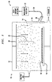
- FIG. 1 particularly illustrates in schematic view a semiconductor wafer processing apparatus 10 according to a preferred embodiment of the invention.
- the semiconductor processing apparatus 10 includes a chamber 12 having an opening with a window 14 therein.
- a substrate holder 16 is positioned within the chamber 12 for holding a semiconductor substrate 18 thereon.
- a plasma generator 20 is located within the chamber 12 for generating a plasma 22 adjacent the semiconductor substrate 18 .
- a remote plasma generator could also be used.
- An optical fiber 28 having opposing first and second ends has the first end positioned adjacent the window 14 such as to be optically coupled to the plasma 22 from outside the chamber 12 , while avoiding reflections from the semiconductor substrate 18 .
- a processor 30 is connected to the second end of the optical fiber 28 for analyzing the plasma.
- the processor 30 preferably includes a plasma etch endpoint detector configured for detecting a semiconductor processing byproduct serving to monitor the endpoint, for example CO.
- the window 14 includes a substantially planar window portion 24 and a substantially tubular window portion 26 extending outwardly therefrom.
- the window 14 is preferably a quartz window for allowing the transmission of light for analysis.
- the tubular window portion 26 has a closed end, and the first end of the optical fiber 28 is connected to the closed end of the tubular window portion 26 .
- the tubular window portion 26 is advantageously positioned at a predetermined angle relative to the planar window portion 24 so as to be optically coupled for viewing the plasma 22 , and to avoid reflections from the semiconductor substrate 18 .
- the predetermined angle may be varied according to requirements of the physical dimensions and structure of the surrounding apparatus, provided the tubular window portion 26 is set at an angle sufficient to exclude reflections from the semiconductor substrate 18 .
- the predetermined angle is about 60 relative to the plane of the planar window portion 24 , and is set so that the tubular window portion 26 is aimed toward an upper part of the chamber 12 .
- the window 14 may be positioned as practicable on the chamber 12 .
- a support bracket 34 is preferably included to secure the connection of the optical fiber 28 to the closed end of the tubular window portion 26 .
- the invention also preferably includes a wavelength selector 32 , also referred to as a monochromator, cooperating with the processor 30 .
- the wavelength selector 32 will be recognized by those skilled in the art to be any one of various devices for selecting the wavelength allowed to pass through for analysis.
- the wavelength selector 32 may be a wavelength filter, an interference filter such as a diffraction grating, or any other such device known in the art.
- the skilled artisan will additionally recognize that the wavelength selector 32 may be positioned relative to the apparatus anywhere practicable for selecting a wavelength for analysis.
- the wavelength selector 32 may be a component of the processor 30 , or it may be separate from the processor and positioned along the optical fiber 28 , or may even be connected between the closed end of the tubular window portion 26 and the first end of the optical fiber 28 .
- the wavelength selector 32 may be fixed to allow transmission of one or more predetermined wavelengths, or may be selectably adjustable to allow passage of one or more selected wavelengths.
- An additional aspect of the invention is directed to a method for semiconductor processing.
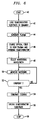
- the method includes the starting process step of loading a semiconductor substrate in the chamber (Block 42 ).
- a plasma is generated within a chamber having a window.
- an optical fiber is coupled adjacent the window such as to be optically coupled to the plasma from outside the chamber, but so as to avoid reflections from the semiconductor substrate.
- the method includes selecting a wavelength for monitoring (Block 48 ), and monitoring emission signals from the optical fiber (Block 50 ). If at Block 52 an endpoint determination is made during monitoring of emissions, then etching is terminated at Block 54 . Monitoring continues until an endpoint is determined. Upon termination of etching, the semiconductor substrate is unloaded from the chamber at Block 56 and the process stops at Block 58 .
Landscapes
- Physics & Mathematics (AREA)
- Engineering & Computer Science (AREA)
- Plasma & Fusion (AREA)
- Chemical & Material Sciences (AREA)
- Analytical Chemistry (AREA)
- Drying Of Semiconductors (AREA)
Abstract
An apparatus for semiconductor processing reduces
etch endpoint interference by analyzing the plasma while
excluding reflections from the semiconductor wafer. The
apparatus includes a chamber having a semiconductor
substrate holder, a plasma generator, and a window. An
optical fiber is connected to the window so as to be
optically connected to the plasma from outside the
chamber. A processor is connected to a second end of the
optical fiber for analyzing the plasma. The window has a
substantially planar portion and a substantially tubular
portion extending outwardly therefrom. The tubular
window portion has a closed end opposite the planar
window portion, and the optical fiber is connected to the
closed end of the tubular window portion. The tubular
window portion is positioned at a predetermined angle
relative to the planar window portion so as to be
optically coupled to view the plasma, while avoiding
reflections from the semiconductor substrate to thereby
reduce the interference.
Description
- The present invention relates to the field of semi-conductor wafer processing and, more particularly, to monitoring plasma etching.
- Plasma etching is a well known dry etching process in the art of semiconductor fabrication. It is also known that the endpoint of a plasma etching process may be determined by monitoring the level of emission of selected byproducts of the etching reaction. For example, an endpoint detector may be used for detecting byproducts of the etched layer in the exhaust stream of the etching chamber. The etching process is stopped when no more byproduct is detected.
- Endpoint detection may also rely on light emitted by the plasma during the etching reaction. This light includes emissions at wavelengths representative of specific substances present in the plasma. Therefore, the level of a reaction byproduct may be monitored through measurement of emissions at the byproduct's particular emission wavelength. By monitoring the level of a byproduct which originates from the layer being removed by the etching, the endpoint of the process is indicated by a sharp drop in the level of emitted reaction product. For example, in a plasma etching process wherein a layer of oxide is being removed, carbon monoxide (CO) is a typical byproduct released into the plasma. CO emits light at a wavelength of 483 nm. Therefore, when the oxide layer is fully removed, the CO emission decreases indicating the endpoint of the etch process.
- In making such emissions measurements, however, it is expected that etching of the oxide layer would appear to proceed at a fairly constant rate. Accordingly, CO emissions would also be expected to be fairly constant. Contrary to the expected result, however, in practice measurement of CO emissions displays a modulation having a period about equal to the time needed for etching a thickness of about half the wavelength used to detect the CO endpoint. This effect has been noted when measuring this byproduct at various wavelengths, so that the effect is independent of the wavelength. Modulation in the measured emission level results in a signal trace having peaks and valleys, making endpoint determination more difficult.
- Experimental evidence indicates that the unexpected modulation in emissions measurements is due to wavelength interference produced by reflection of light from at least two levels on the wafer. Photons from the plasma are partially reflected and transmitted at the wafer surface. Photons reflected at the wafer surface produce a first reflection. The transmitted photons are then reflected at the silicon interface, forming a second reflection. The difference in the length of the optical paths for the first and second reflections produces an interference between the two reflections. When the extra distance traveled by the second reflection is an even multiple of one fourth of the wavelength, the interference is constructive. When the extra distance of travel is an odd multiple, the interference is destructive. This interference effect explains the inconsistent behavior of the signals observed.
- The interference makes endpoint determination more difficult because an apparent drop in the emission being measured may be an artifact due to the modulation effect, rather than a true decrease indicating the endpoint of the etching process. This uncertainty causes an imprecise endpoint determination and contributes to reduced accuracy and quality control problems in the etching process.
- In view of the foregoing background, it is therefore an object of the invention to provide an apparatus and method for increasing the precision of endpoint determinations in a plasma etching process for semiconductor wafer fabrication.
- It is another object of the present invention to provide etch endpoint determinations which are consistent and reproducible as required in a semiconductor production environment.
- These and other objects, features and advantages in accordance with the present invention are provided by a semiconductor processing apparatus which eliminates this interference by analyzing the plasma while excluding reflections from the semiconductor wafer. The apparatus includes a chamber having a window. The chamber has a substrate holder within for holding a semiconductor substrate. The chamber, which is a plasma etching chamber, also includes a plasma generator for generating a plasma within the chamber. An optical fiber having opposing first and second ends, is positioned adjacent the window such that the first end is optically coupled to the plasma from outside the chamber. However, the optical fiber is positioned to avoid reflections from the semiconductor substrate. A processor is connected to the second end of the optical fiber for analyzing the plasma.
- In a preferred embodiment, the chamber window has a substantially planar portion and a substantially tubular portion extending outwardly therefrom. The tubular window portion has a closed end opposite the planar window portion. The first end of the optical fiber is connected to the closed end of the tubular window portion. Advantageously, the tubular window portion is positioned at a predetermined angle relative to the planar window portion so as to be optically coupled to view the plasma, while avoiding reflections from the semiconductor substrate to thereby eliminate the interference. Any angle sufficient to avoid reflections from the wafer may be employed in the apparatus, with an angle of about 60 from the planar window portion being a preferred angle.
- A method aspect of the invention for semiconductor processing includes generating a plasma within a chamber having a window, connecting an optical fiber to the window so as to be optically coupled to the plasma while avoiding reflections from the semiconductor substrate, and processing signals from the optical fiber for analysis of the plasma.
- Some of the features, advantages, and benefits of the present invention having been stated, others will become apparent as the description proceeds when taken in conjunction with the accompanying drawings in which:
- FIG. 1 is a schematic cross-sectional view of the semiconductor processing apparatus in accordance with the present invention;
- FIG. 2 is a top plan view of the window of the apparatus shown in FIG. 1;
- FIG. 3 is a cross-section taken along lines 3-3 of FIG. 2;
- FIG. 4 is a top plan view of the supporting bracket of the apparatus shown in FIG. 1;
- FIG. 5 is a cross-section taken along lines 5-5 of FIG. 4; and
- FIG. 6 is a flow chart of a method according to an embodiment of the present invention.
-
- The present invention will now be described more fully hereinafter with reference to the accompanying drawings, in which preferred embodiments of the invention are shown. This invention may, however, be embodied in many different forms and should not be construed as limited to the illustrated embodiments set forth herein. Rather, these illustrated embodiments are provided so that this disclosure will be thorough and complete, and will fully convey the scope of the invention to those skilled in the art.
- Various aspects of the present invention are seen illustrated in FIGS. 1-4. FIG. 1 particularly illustrates in schematic view a semiconductor
wafer processing apparatus 10 according to a preferred embodiment of the invention. Thesemiconductor processing apparatus 10 includes achamber 12 having an opening with a window 14 therein. Asubstrate holder 16 is positioned within thechamber 12 for holding asemiconductor substrate 18 thereon. Aplasma generator 20 is located within thechamber 12 for generating aplasma 22 adjacent thesemiconductor substrate 18. Of course, a remote plasma generator could also be used. - An
optical fiber 28 having opposing first and second ends, has the first end positioned adjacent the window 14 such as to be optically coupled to theplasma 22 from outside thechamber 12, while avoiding reflections from thesemiconductor substrate 18. Aprocessor 30 is connected to the second end of theoptical fiber 28 for analyzing the plasma. Theprocessor 30 preferably includes a plasma etch endpoint detector configured for detecting a semiconductor processing byproduct serving to monitor the endpoint, for example CO. - In a preferred embodiment of the
apparatus 10, the window 14 includes a substantiallyplanar window portion 24 and a substantiallytubular window portion 26 extending outwardly therefrom. The window 14, is preferably a quartz window for allowing the transmission of light for analysis. Thetubular window portion 26 has a closed end, and the first end of theoptical fiber 28 is connected to the closed end of thetubular window portion 26. Thetubular window portion 26 is advantageously positioned at a predetermined angle relative to theplanar window portion 24 so as to be optically coupled for viewing theplasma 22, and to avoid reflections from thesemiconductor substrate 18. Those skilled in the art will understand that the predetermined angle may be varied according to requirements of the physical dimensions and structure of the surrounding apparatus, provided thetubular window portion 26 is set at an angle sufficient to exclude reflections from thesemiconductor substrate 18. In a preferred embodiment as shown schematically in FIG. 1, the predetermined angle is about 60 relative to the plane of theplanar window portion 24, and is set so that thetubular window portion 26 is aimed toward an upper part of thechamber 12. The skilled artisan will appreciate that the window 14 may be positioned as practicable on thechamber 12. In addition, as shown in FIGS. 4 and 5, asupport bracket 34 is preferably included to secure the connection of theoptical fiber 28 to the closed end of thetubular window portion 26. - The invention also preferably includes a
wavelength selector 32, also referred to as a monochromator, cooperating with theprocessor 30. Thewavelength selector 32 will be recognized by those skilled in the art to be any one of various devices for selecting the wavelength allowed to pass through for analysis. Thewavelength selector 32 may be a wavelength filter, an interference filter such as a diffraction grating, or any other such device known in the art. The skilled artisan will additionally recognize that thewavelength selector 32 may be positioned relative to the apparatus anywhere practicable for selecting a wavelength for analysis. For example, thewavelength selector 32 may be a component of theprocessor 30, or it may be separate from the processor and positioned along theoptical fiber 28, or may even be connected between the closed end of thetubular window portion 26 and the first end of theoptical fiber 28. Furthermore, thewavelength selector 32 may be fixed to allow transmission of one or more predetermined wavelengths, or may be selectably adjustable to allow passage of one or more selected wavelengths. - An additional aspect of the invention, as explained with reference to FIG. 6, is directed to a method for semiconductor processing. From the start (Block 40) the method includes the starting process step of loading a semiconductor substrate in the chamber (Block 42). At Block 44 a plasma is generated within a chamber having a window. At
Block 46 an optical fiber is coupled adjacent the window such as to be optically coupled to the plasma from outside the chamber, but so as to avoid reflections from the semiconductor substrate. Subsequently, the method includes selecting a wavelength for monitoring (Block 48), and monitoring emission signals from the optical fiber (Block 50). If atBlock 52 an endpoint determination is made during monitoring of emissions, then etching is terminated atBlock 54. Monitoring continues until an endpoint is determined. Upon termination of etching, the semiconductor substrate is unloaded from the chamber atBlock 56 and the process stops atBlock 58. - Many modifications and other embodiments of the invention will come to the mind of one skilled in the art, having the benefit of the teachings presented in the foregoing descriptions and the associated drawings. Therefore, it is to be understood that the invention is not to be limited to the specific embodiments disclosed, and that modifications and embodiments are intended to be included within the scope of the appended claims.
Claims (23)
- A semiconductor processing apparatus comprising:a chamber having an opening therein;a window in the opening of said chamber;a substrate holder within said chamber for holding a semiconductor substrate thereon;a plasma generator for generating a plasma within said chamber and adjacent the semiconductor substrate;an optical fiber having opposing first and second ends, the first end positioned adjacent said window such as to be optically coupled to the plasma from outside said chamber while avoiding reflections from the semiconductor substrate; anda processor connected to the second end of said optical fiber for analyzing the plasma.
- A semiconductor processing apparatus according to Claim 1 wherein said processor comprises a plasma etch endpoint detector.
- A semiconductor processing apparatus according to Claim 1 or Claim 2 wherein said window comprises a substantially planar window portion and a substantially tubular window portion extending outwardly therefrom.
- A semiconductor processing apparatus according to Claim 3 wherein said tubular window portion has a closed end opposite said planar window portion, and wherein the first end of said optical fiber is positioned adjacent to the closed end of said tubular window portion.
- A semiconductor processing apparatus according to Claim 4 wherein the first end of the optical fiber is connected to the closed end of said tubular window portion.
- A semiconductor processing apparatus according to any of claims 3 to 5 wherein said tubular window portion is positioned at a predetermined angle relative to said planar window portion so as to be optically coupled to view the plasma and while avoiding reflections from the semiconductor substrate.
- A semiconductor processing apparatus according to Claim 6 wherein the predetermined angle of said tubular portion is about 60 degrees.
- A semiconductor processing apparatus according to any of the preceding claims, further comprising a wavelength selector positioned to select light wavelength corresponding to a semiconductor processing byproduct for analysis by the processor.
- A semiconductor processing apparatus according to Claim 8, wherein said processor further comprises the wavelength selector.
- A semiconductor processing apparatus according to any of the preceding claims wherein said window comprises quartz.
- A semiconductor processing apparatus according to any of the preceding claims wherein said processor is for detecting a semiconductor processing byproduct in the plasma.
- A semiconductor processing apparatus according to Claim 11 wherein said byproduct is carbon monoxide.
- A semiconductor processing apparatus according to any of the preceding claims wherein said window is positioned in a sidewall of said chamber.
- A semiconductor processing apparatus according to any of the preceding claims further comprising a supporting bracket positioned for supporting the optical fiber adjacent the closed end of the tubular window portion.
- A method for semiconductor processing comprising the steps of:generating a plasma within a chamber having a window therein:coupling an optical fiber adjacent the window such as to be optically coupled to the plasma from outside the chamber while avoiding reflections from the semiconductor substrate; andprocessing signals from the optical fiber.
- The method of Claim 15, wherein the step of processing signals comprises detecting a plasma etch endpoint.
- The method of Claim 15 or Claim 16, wherein the window comprises a substantially planar window portion and a tubular window portion extending outwardly therefrom.
- The method of Claim 17 wherein the tubular window portion has a closed end opposite the planar window portion, and wherein the step of coupling an optical fiber includes connecting a first end of the optical fiber to the closed end of the tubular window portion.
- The method of Claim 17 or Claim 18 further including the step of positioning the tubular window portion at a predetermined angle relative to the planar window portion so as to be optically coupled to view the plasma while avoiding reflections from the semiconductor substrate.
- The method of Claim 19 wherein the predetermined angle of the tubular portion is 60 degrees.
- The method of any of Claims 15 to 20 wherein the step of processing signals further includes passing the signals through a wavelength selector.
- The method of any of Claims 15 to 21 wherein the step of processing signals further includes detecting a semiconductor processing byproduct in the plasma.
- The method of Claim 22 wherein the semiconductor processing byproduct detected is essentially CO.
Applications Claiming Priority (2)
| Application Number | Priority Date | Filing Date | Title |
|---|---|---|---|
| US09/432,926 US6358359B1 (en) | 1999-11-03 | 1999-11-03 | Apparatus for detecting plasma etch endpoint in semiconductor fabrication and associated method |
| US432926 | 1999-11-03 |
Publications (1)
| Publication Number | Publication Date |
|---|---|
| EP1098352A2 true EP1098352A2 (en) | 2001-05-09 |
Family
ID=23718137
Family Applications (1)
| Application Number | Title | Priority Date | Filing Date |
|---|---|---|---|
| EP00309334A Withdrawn EP1098352A2 (en) | 1999-11-03 | 2000-10-23 | Apparatus for detecting plasma etch endpoint and method |
Country Status (2)
| Country | Link |
|---|---|
| US (1) | US6358359B1 (en) |
| EP (1) | EP1098352A2 (en) |
Cited By (1)
| Publication number | Priority date | Publication date | Assignee | Title |
|---|---|---|---|---|
| SG87924A1 (en) * | 2000-03-31 | 2002-04-16 | Applied Materials Inc | Monitoring a effluent from a chamber |
Families Citing this family (6)
| Publication number | Priority date | Publication date | Assignee | Title |
|---|---|---|---|---|
| EP1265278A1 (en) * | 2001-06-06 | 2002-12-11 | Infineon Technologies AG | Method for manufacturing a trench capacitor with an isolation trench |
| US6888639B2 (en) * | 2001-09-24 | 2005-05-03 | Applied Materials, Inc. | In-situ film thickness measurement using spectral interference at grazing incidence |
| US6930782B1 (en) * | 2003-03-28 | 2005-08-16 | Lam Research Corporation | End point detection with imaging matching in semiconductor processing |
| US7300594B2 (en) * | 2003-06-27 | 2007-11-27 | The Procter & Gamble Company | Process for purifying a lipophilic fluid by modifying the contaminants |
| US9997325B2 (en) * | 2008-07-17 | 2018-06-12 | Verity Instruments, Inc. | Electron beam exciter for use in chemical analysis in processing systems |
| KR102833984B1 (en) | 2020-08-31 | 2025-07-15 | 삼성전자주식회사 | Monitoring method of semiconductor device and manufacturing method of semiconductor device including the same |
Family Cites Families (8)
| Publication number | Priority date | Publication date | Assignee | Title |
|---|---|---|---|---|
| US5208644A (en) | 1990-05-18 | 1993-05-04 | Xinix, Inc. | Interference removal |
| US5499733A (en) | 1992-09-17 | 1996-03-19 | Luxtron Corporation | Optical techniques of measuring endpoint during the processing of material layers in an optically hostile environment |
| US5728253A (en) * | 1993-03-04 | 1998-03-17 | Tokyo Electron Limited | Method and devices for detecting the end point of plasma process |
| US5891352A (en) | 1993-09-16 | 1999-04-06 | Luxtron Corporation | Optical techniques of measuring endpoint during the processing of material layers in an optically hostile environment |
| KR0152355B1 (en) * | 1994-03-24 | 1998-12-01 | 가나이 쓰토무 | Plasma treatment apparatus and treatment method |
| JP3193265B2 (en) | 1995-05-20 | 2001-07-30 | 東京エレクトロン株式会社 | Plasma etching equipment |
| US5846373A (en) | 1996-06-28 | 1998-12-08 | Lam Research Corporation | Method for monitoring process endpoints in a plasma chamber and a process monitoring arrangement in a plasma chamber |
| JPH11176815A (en) * | 1997-12-15 | 1999-07-02 | Ricoh Co Ltd | Dry etching end point determination method and dry etching apparatus |
-
1999
- 1999-11-03 US US09/432,926 patent/US6358359B1/en not_active Expired - Lifetime
-
2000
- 2000-10-23 EP EP00309334A patent/EP1098352A2/en not_active Withdrawn
Cited By (1)
| Publication number | Priority date | Publication date | Assignee | Title |
|---|---|---|---|---|
| SG87924A1 (en) * | 2000-03-31 | 2002-04-16 | Applied Materials Inc | Monitoring a effluent from a chamber |
Also Published As
| Publication number | Publication date |
|---|---|
| US6358359B1 (en) | 2002-03-19 |
Similar Documents
| Publication | Publication Date | Title |
|---|---|---|
| USRE39145E1 (en) | Method and apparatus for in-situ monitoring of plasma etch and deposition processes using a pulsed broadband light source | |
| EP0735565B1 (en) | Method and apparatus for monitoring the dry etching of a dielectric film to a given thickness | |
| JP4925507B2 (en) | Film thickness control using spectral interferometry | |
| US6745095B1 (en) | Detection of process endpoint through monitoring fluctuation of output data | |
| JPH0786254A (en) | Semiconductor manufacturing apparatus and semiconductor manufacturing method | |
| US20110090503A1 (en) | Apparatus for detecting arcs | |
| US6062729A (en) | Rapid IR transmission thermometry for wafer temperature sensing | |
| TWI758478B (en) | Polishing apparatus and polishing method | |
| WO2003027609A1 (en) | In-situ film thickness measurement using spectral interference at grazing incidence | |
| US5208644A (en) | Interference removal | |
| US20080078948A1 (en) | Processing termination detection method and apparatus | |
| WO1998058400A2 (en) | Liquid etch endpoint detection and process metrology | |
| US6358359B1 (en) | Apparatus for detecting plasma etch endpoint in semiconductor fabrication and associated method | |
| US8014891B2 (en) | Etching amount calculating method, storage medium, and etching amount calculating apparatus | |
| US10260868B2 (en) | Interferometric method and system using variable fringe spacing for inspecting transparent wafers for electronics, optics or optoelectronics | |
| US7227624B2 (en) | Method and apparatus for monitoring the condition of plasma equipment | |
| US6650426B1 (en) | Endpoint determination for recess etching to a precise depth | |
| JP2001194320A (en) | Surface condition measuring device and method | |
| US6750977B2 (en) | Apparatus for monitoring thickness of deposited layer in reactor and dry processing method | |
| US20040005727A1 (en) | Device and method for automatically determining the surface quality of a bonding interface between two wafers | |
| CN1554107A (en) | Shallow-angle interferometry process and apparatus for determining real-time etch rates | |
| TWI898234B (en) | System and method for fault detection and operational readiness for optical instruments for semiconductor processes | |
| JPH1064884A (en) | Etching apparatus and etching method | |
| US6450683B1 (en) | Optical temperature measurement as an in situ monitor of etch rate | |
| JPH0518454B2 (en) |
Legal Events
| Date | Code | Title | Description |
|---|---|---|---|
| PUAI | Public reference made under article 153(3) epc to a published international application that has entered the european phase |
Free format text: ORIGINAL CODE: 0009012 |
|
| AK | Designated contracting states |
Kind code of ref document: A2 Designated state(s): AT BE CH CY DE DK ES FI FR GB GR IE IT LI LU MC NL PT SE |
|
| AX | Request for extension of the european patent |
Free format text: AL;LT;LV;MK;RO;SI |
|
| STAA | Information on the status of an ep patent application or granted ep patent |
Free format text: STATUS: THE APPLICATION IS DEEMED TO BE WITHDRAWN |
|
| 18D | Application deemed to be withdrawn |
Effective date: 20021101 |