EP1098259A2 - Rate equation method and apparatus for simulation of current in a mos device - Google Patents
Rate equation method and apparatus for simulation of current in a mos device Download PDFInfo
- Publication number
- EP1098259A2 EP1098259A2 EP00309335A EP00309335A EP1098259A2 EP 1098259 A2 EP1098259 A2 EP 1098259A2 EP 00309335 A EP00309335 A EP 00309335A EP 00309335 A EP00309335 A EP 00309335A EP 1098259 A2 EP1098259 A2 EP 1098259A2
- Authority
- EP
- European Patent Office
- Prior art keywords
- source
- channel
- region
- values
- voltage
- Prior art date
- Legal status (The legal status is an assumption and is not a legal conclusion. Google has not performed a legal analysis and makes no representation as to the accuracy of the status listed.)
- Granted
Links
Images


Classifications
-
- H—ELECTRICITY
- H10—SEMICONDUCTOR DEVICES; ELECTRIC SOLID-STATE DEVICES NOT OTHERWISE PROVIDED FOR
- H10D—INORGANIC ELECTRIC SEMICONDUCTOR DEVICES
- H10D84/00—Integrated devices formed in or on semiconductor substrates that comprise only semiconducting layers, e.g. on Si wafers or on GaAs-on-Si wafers
- H10D84/80—Integrated devices formed in or on semiconductor substrates that comprise only semiconducting layers, e.g. on Si wafers or on GaAs-on-Si wafers characterised by the integration of at least one component covered by groups H10D12/00 or H10D30/00, e.g. integration of IGFETs
- H10D84/82—Integrated devices formed in or on semiconductor substrates that comprise only semiconducting layers, e.g. on Si wafers or on GaAs-on-Si wafers characterised by the integration of at least one component covered by groups H10D12/00 or H10D30/00, e.g. integration of IGFETs of only field-effect components
- H10D84/83—Integrated devices formed in or on semiconductor substrates that comprise only semiconducting layers, e.g. on Si wafers or on GaAs-on-Si wafers characterised by the integration of at least one component covered by groups H10D12/00 or H10D30/00, e.g. integration of IGFETs of only field-effect components of only insulated-gate FETs [IGFET]
- H10D84/85—Complementary IGFETs, e.g. CMOS
-
- G—PHYSICS
- G06—COMPUTING OR CALCULATING; COUNTING
- G06F—ELECTRIC DIGITAL DATA PROCESSING
- G06F30/00—Computer-aided design [CAD]
- G06F30/30—Circuit design
- G06F30/36—Circuit design at the analogue level
- G06F30/367—Design verification, e.g. using simulation, simulation program with integrated circuit emphasis [SPICE], direct methods or relaxation methods
Definitions
- the present invention relates generally to measuring electrical behavior in semi-conductor devices and relates more particularly, to simulating current in MOSFET devices based on an improved barrier model rate equation.
- a semiconductor device such as a MOSFET, having a source region, a gate region, a drain region and a channel region associated with it, have been successfully modeled in the past.
- the dimensions of these associated regions necessarily decrease.
- classical transport concepts such as drift, diffusion, or other quantities become less reliable. Consequently, the transport equations used to model these devices, and which rely on these factors, are of limited accuracy. Thus they lose their useful in the simulation and design of smaller MOSFETs.
- the instant invention demonstrates the viability of modeling the current in a short-channel MOSFET without the use of mobility, diffusion or classical electron velocity. Such a model is useful where the uncertainty in the velocity of electrons that traverse the channel becomes comparable to the saturation velocity of electrons in the device. This unfavorable characteristic is present in silicon-based metal-oxide semiconductor field-effect transistors (MOSFETs) currently manufactured.
- MOSFETs metal-oxide semiconductor field-effect transistors
- the instant rate-equation model is particularly useful for short-channel MOSFETs, where comparable transport equations have not previously been applied. Results, including current-voltage (I-V) characteristics generated by the instant rate equation (or barrier model), compare well qualitatively to experimental data, as well as to results from electrical device computer simulation programs such as PADRE or SPICE.
- the instant barrier model replicates features of the current-voltage curve that are often ascribed to variations in the mobility, although mobility is not included in the rate equation.
- a method for determining a current-voltage characteristic for a semiconductor device having a source region, a drain region and a channel region comprises: assigning one of a plurality of fixed values to each of at least one of a plurality of model variables including a gate-to-source voltage (V GS ) to be applied to the device, a drain-to source voltage (V DS ) to be applied to the device, a first Fermi level (F 1 ) corresponding to the source region of the device, a second Fermi level (F 2 ) corresponding to the channel region of the device, a width (W) of the channel region, an operating temperature (T) of the device, a quantization energy level (E qv ) of the device, a height (Vo) of a source-channel barrier of the device, and a mass in a z-direction for electrons in a channel valley (m zv ); assigning a plurality of differing values for each of the
- a computer-readable medium encoded with processing instructions for implementing a method, performed by a computer, for simulating current-voltage behavior in a semiconductor device having a source region, a channel region and a drain region, the method comprising: receiving an input including one of a plurality of fixed values for each of at least one of a plurality of model variables including a gate-to-source voltage (V GS ) to be applied to the device, a drain-to source voltage (V DS ) to be applied to the device, a first Fermi level (F 1 ) corresponding to the source region of the device, a second Fermi level (F 2 ) corresponding to the channel region of the device, a width (W) of the channel region, an operating temperature (T) of the device, a quantization energy level (E qv ) of the device, a height (Vo) of a source-channel barrier of the device, and a mass in a z-direction for electron
- V GS gate-to-source voltage
- an apparatus for simulating current-voltage behavior in a semiconductor device having a source region, a channel region and a drain region comprises: a processor; a memory connected to the processor, the memory storing a program to control the operation of the processor; and the processor operative with the program to: receive an input including one of a plurality of fixed values for each of at least one of a plurality of model variables including a gate-to-source voltage (V GS ) to be applied to the device, a drain-to source voltage (V DS ) to be applied to the device, a first Fermi level (F 1 ) corresponding to the source region of the device, a second Fermi level (F 2 ) corresponding to the channel region of the device, a width (W) of the channel region, an operating temperature (T) of the device, a quantization energy level (E qv ) of the device, a height (Vo) of a source-channel barrier of the device, and a mass
- Disclosed herein is a new method of calculating the current in a short-channel MOS device.
- the results of the disclosed method have been favorably compared against conventional simulation programs, as well as with actual measurements taken from n-type MOS devices.
- the maximum physical uncertainty in the location of its wave packet, ⁇ x is the channel length L. Since the classical distribution function is specified by the simultaneous position (x) and momentum (p) of electrons in the channel, ⁇ x must in fact be much less than the gate length. The velocity of an electron is calculated as p/m, where m is the effective mass of the electron. Thus, ⁇ v must equal ⁇ p/m . Incorporating the Heisenberg relation, it is found that the minimum ⁇ v is h/m ⁇ x .
- the barrier model rate equation of the present invention avoids the above difficultly.
- the rate-limiting step in electron transport in a MOS device is the jump across the source-channel barrier shown schematically in Fig. 1. This barrier arises because of the doping difference between source and channel.
- a barrier model rate equation of the present invention is then derived generally according to the following principles: First, the mean rate of electron transfer from a state in the source to a state in the channel is proportional to the probability that the initial state is occupied and the final state is empty. Next, both forward and reverse current velocity are calculated, whereafter it is demonstrated that their proportionality constants are related. The total current is then found by summing over all possible pairs of transitions across the barrier.
- results from the barrier model rate equation disclosed below have been compared to results from the device simulator PADRE, and data from 200-micron wide NMOS devices with gate lengths between 0.1 and 0.25 microns.
- results from the barrier model rate equation disclosed below have been compared to results from the device simulator PADRE, and data from 200-micron wide NMOS devices with gate lengths between 0.1 and 0.25 microns.
- the dominant features of the resulting current-voltage characteristic according to the barrier model qualitatively agree with the results of the PADRE simulator.
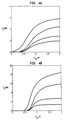
- Figs. 4(a)-4(c) demonstrate, there is some quantitative discrepancy due to uncertainty in the dopant concentration of the device that was tested.
- the simplified model disclosed herein produces an incorrect magnitude for the current, it yields useful analytical results that produce physical insight into the behavior of MOS devices. Such qualitative characteristics are useful, for example, in simulating a MOS device design prior to manufacture.
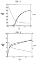
- Fig. 2 displays a two-dimensional graph of an I-V characteristic generated through a PADRE simulation and by the instant model.
- the source-channel barrier height vs gate bias (V gs ) from PADRE is plotted as a dashed line. This value was used to calculate the current in the barrier, which is plotted as a solid line in Fig. 2.
- the value of the current from PADRE shown by a dot-dashed line in Fig. 2, is scaled by a constant factor (of approximately 5) in order to show the similarity of the curves as predicted by the PADRE simulation and the instant model.
- the graph reveals that the saturating behavior of the barrier height with increasing V gs causes the current to saturate. This effect is conventionally ascribed to a reduction in mobility due to increased interface roughness scattering.
- the barrier model demonstrates the physical characteristics ascribed to mobility without taking such factor into account explicitly.
- Fig. 3 the same three quantities are plotted as a function of drain bias V ds .
- the dashed line is the value of the barrier height from PADRE
- the solid line is the resulting current in the barrier model
- the dot-dashed line is the calculated current from PADRE.
- the output conductance corresponds to the degree to which the drain bias changes the barrier height.
- Figs. 4(a) and (b) Calculations for the barrier-dominated model and actual measurements of I d vs.V ds are shown in Figs. 4(a) and (b), respectively, for devices with gate widths of 200 microns, and gate lengths of 0.10, 0.15, 0.20 and 0.25 microns.
- the PADRE-calculated currents are shown in Fig. 4(c).
- the barrier height was estimated with some factor of quantitative uncertainty. More accurate knowledge of this parameter would improve the quantitative agreement between the barrier model and the data.
- the barrier model yields a current that depends exponentially on the source-channel barrier height and produces qualitatively correct behavior despite several simplifying assumptions.
- the resulting analytical expression is of a complexity that would be suitable for circuit analysis.
- a MOS device under bias has the band structure shown schematically in Fig 1.
- Fig 1 there is a barrier which forms due to the difference in doping between the source and the channel. Since the current must be continuous, the current can be calculated at a point near the barrier in the channel. Electrons that have left the source and are traveling in the channel will quickly accelerate to saturated velocities when the source-drain bias is significant. As a consequence, electron transport is quite rapid in the channel. However, before the electron reaches the source-drain field region, it must traverse from the source into the channel. Assuming the electrons in the source are thermally distributed, some number of electrons will have an insufficient amount of energy to traverse the barrier. Others will have a minimum energy, and then there will be an exponential decrease as the energy is increased in the number of carriers.
- an electron's velocity can be written as h k x /m x *, where k is a wave vector associated with an electron and having components k x , k y and k z . (See FIG. 1 for the direction definitions). Since k , can be arbitrarily small, some electrons will take an arbitrarily long time to traverse the barrier. Others which are higher in energy will cross more rapidly, but very few will traverse the barrier at the saturated velocity.
- barrier model variables have the following meanings:
- R 1-2 ( W/ 2 ⁇ 2 ) v ⁇ d k x d k z (h k x / m xv ) f 1 ( l-f 2 )
- W is the width of the device
- f is the occupation of the state with energy corresponding to h and k , in region n.
- the summation over the valley region (v) accounts for the different band minima and different sub-bands in the potential well at the surface.
- R 2-1 ( W/2 ⁇ 2 ) v ⁇ d k x d k z ( h k x /m xv ) f 2 ( l-f 1 ) It will be assumed that the electrons in region 1 are in quasi-equilibrium with the source. The electrons in region 2 are being swept into the channel, so it follows that they have a different Fermi level from electrons in region 1. Depending on the transition rate back and forth across the barrier, these approximation will have varying degrees of accuracy. However, within the limit of this model, all electrons crossing the barrier from region 1 to region 2 continue on into the channel.
- the Fermi level in region 2 is much less than that in region 1 when the channel is under bias.
- the states that the electrons are entering once crossing the barrier are essentially unoccupied.
- the denominator of the above equation is dominated by e (E-F 1 )/kT .
- the total current is then approximated by: I 12 ⁇ (2 qW /(2 ⁇ ) 2 )(1- e ( F 2- F 1)kT ) v ⁇ d k x d k z ( h k x m xv ) e ( F 1- E )/ kT
- E E qv +V o +( h 2 /2)(( k x 2 /m xv )+( k z 2 /m zv ))
- Eqv is the energy of quantitization for the v valley.
- I 12 (2 qW h/(2 ⁇ ) 2 )( I - e ( F 2- F 1)/ kT ) v ( e ( F 1- Eqv - Vo / kt ) / m xv ) - ⁇ ⁇ o ⁇ d k x d k z k z exp (-h 2 x /2 kT ) ( k 2 x / m xv )+( k 2 z / m zv )
- a designer may input a plurality of different variables into the above equation to achieve a desirable I-V characteristic for a contemplated MOS device. It is contemplated that such derivations may readily be performed on a computer.
- Computer system 90 is operative to receive program instructions and user inputs, and is further operative to output results corresponding to such instructions and inputs in accordance with the present invention.
- Computer system 90 comprises a central processing unit (processor) 100 which may be any commonly available microprocessor such as the PENTIUM III manufactured by INTEL CORP.
- Processor 100 is operatively connected to RAM/ROM 102, clock 104, data storage device 106 (which stores program 107), input device(s) 108 and output device(s) 110.
- Random-access memory may be a suitable number of Single In-line Memory Module (SIMM) chips having a storage capacity (typically measured in megabytes) sufficient to store, inter alia, processing instructions utilized by processor 100 during operation of computer system 90.
- RAM Random-access memory
- ROM Read-only memory
- RAM/ROM 102 Further functions of RAM/ROM 102 will be apparent to one of ordinary skill in the art.
- Clock 104 may be an on-board component of processor 100 which dictates a clock speed (typically measured in MHz) at which processor 100 performs and synchronizes communication between hardware components of computer system 90. Further functions of clock 104 will be apparent to one of ordinary skill in the art.
- Input device(s) 108 may be one or more commonly known devices used for communicating information to computer system 90 via either another computer system or by user inputs. Accordingly, input device(s) 108 may include a keyboard, a mouse, a graphics tablet, a scanner, a voice recognition unit, a parallel or serial communication port, a network connection and any appropriate network or other communication card for receiving data. Input device(s) 108 is/are operative to allow a user to input instructions and values in accordance with the present invention.
- Output device(s) 110 may be one or more commonly known devices used by computer system 90 to communicate the results of inputted instructions and values to a user of computer system 90. Accordingly, output device(s) 110 may include a display monitor, a voice synthesizer, a printer, a parallel or serial communication port, a network connection and any appropriate network or other communication card for sending data. Output device(s) 110 is/are operative to allow a user to receive the results of input instructions and values in accordance with the present invention.
- Data storage device 106 may be either an internal or external large capacity memory for storing computer data, the storage capacity of which is typically measured in gigabytes.
- Data storage device 106 stores, inter alia, an operating system such as WINDOWS NT by MICROSOFT CORP, and one or more application programs, such as program 107.
- data storage device 106 may be one or more of the following: a floppy disk drive, a hard disk drive, a CD-ROM disk and reader/writer, a DVD disk and reader/writer, a ZIP disk and a ZIP drive of the type manufactured by IOMEGA CORP., and/or any other computer readable medium that may be encoded with processing instructions in a read-only or read-write format. Further functions of and available devices for data storage device 106 will be apparent to one of ordinary skill in the art.
- Program 107 includes a plurality of processing instructions which enables computer system 90 to receive inputs of data and information and determine voltage-current characteristics of a MOS device in accordance with the present invention.
- Program 107 may be written in any conventional computer language that is comprehensible to computer system 90, such as C++.
- Program 107 preferably includes processing instructions allowing computer system 90 to accept inputs of barrier model variables and/or to select appropriate values for the barrier model variables.
- Program 107 also preferably includes processing instructions allowing computer system 90 to determine the results for each of the variety of input and selected variables, the results including a current value for each of the input values that results from the barrier model rate equation disclosed herein.
- program 107 preferably includes processing instructions allowing computer system 90 to generate an I-V characteristic of an MOS device exhibiting properties represented by the input variables.
- I-V characteristic is typically a plot of a curve of current values versus voltage values on a standard two dimensional graph, as exemplified in Figs. 4(a)-4(c).
- the I-V characteristic may be presented to a user via any of the output device(s) 110 contemplated for use with a computer system 90.
Landscapes
- Engineering & Computer Science (AREA)
- Computer Hardware Design (AREA)
- Physics & Mathematics (AREA)
- Theoretical Computer Science (AREA)
- Microelectronics & Electronic Packaging (AREA)
- Evolutionary Computation (AREA)
- Geometry (AREA)
- General Engineering & Computer Science (AREA)
- General Physics & Mathematics (AREA)
- Insulated Gate Type Field-Effect Transistor (AREA)
Abstract
Description
Claims (14)
- A method for determining a current-voltage characteristic for a semiconductor device having a source region, a drain region and a channel region, the method comprising:assigning one of a plurality of fixed values to each of at least one of a plurality of barrier model variables including a gate-to-source voltage (VGS) to be applied to the device, a drain-to source voltage (VDS) to be applied to the device, a first Fermi level (F1) corresponding to the source region of the device, a second Fermi level (F2) corresponding to the channel region of the device, a width (W) of the channel region, an operating temperature (T) of the device, a quantization energy level (Eqv) of the device, a height (Vo) of a source-channel barrier of the device, and a mass in a z-direction for an electron in a valley (mzv);assigning a plurality of differing values for each of the remaining barrier model variables; anddetermining, for each of the plurality of differing values, a current value (I12) from a rate equation modeled after the source-channel barrier.
- The method according to claim 1 wherein the rate equation comprises:
- The method according to claim 1, further comprising:determining a current-voltage characteristic from a plurality of determined current values (I12) and a plurality of voltage values.
- The method according to claim 3, wherein the plurality of voltage values comprise a plurality of values for the gate-to-source voltage (VGS).
- The method according to claim 4, wherein the value of the drain-to-source voltage (VDS) is held constant.
- The method according to claim 3, wherein the plurality of voltage values comprise a plurality of values for the drain-to-source voltage (VDS).
- The method according to claim 6, wherein the value of the gate-to-source voltage (VGS) is held constant.
- The method of claim 3, further comprising:deriving a second current-voltage characteristic by assigning a second one of a plurality of fixed values to each of at least one of a plurality of model variables; andassigning a plurality of differing values for each of the remaining model variables.
- The method of claim 1, wherein the device is a metal-oxide semiconductor field-effect transistor.
- A computer-readable medium encoded with processing instructions for implementing a method, performed by a computer, for simulating current-voltage behavior in a semiconductor device having a source region, a channel region and a drain region, the method comprising:receiving an input including one of a plurality of fixed values for each of at least one of a plurality of model variables including a gate-to-source voltage (VGS) to be applied to the device, a drain-to source voltage (VDS) to be applied to the device, a first Fermi level (F1) corresponding to the source region of the device, a second Fermi level (F2) corresponding to the channel region of the device, a width (W) of the channel region, an operating temperature (T) of the device, a quantization energy level (Eqv) of the device, a height (Vo) of a source-channel barrier of the device, and a mass in a z-direction for an electron in a channel valley (mzv);assigning a plurality of differing values for each of the remaining model variables; anddetermining, for each of the plurality of differing values, a current value (I12) from a rate equation modeled after the source-channel barrier.
- The computer-readable medium according to claim 1 wherein the rate equation comprises:
- An apparatus for simulating current-voltage behavior in a semiconductor device having a source region, a channel region and a drain region, comprising:a processor;a memory connected to the processor, the memory storing a program to control the operation of the processor; andthe processor being operative with the program to:receive an input including one of a plurality of fixed values for each of at least one of a plurality of model variables including a gate-to-source voltage (VGS) to be applied to the device, a drain-to source voltage (VDS) to be applied to the device, a first Fermi level (F1) corresponding to the source region of the device, a second Fermi level (F2) corresponding to the channel region of the device, a width (W) of the channel region, an operating temperature (T) of the device, a quantization energy level (Eqv) of the device, a height (Vo) of a source-channel barrier of the device, and a mass in a z-direction for an electron in a channel valley (mzv);assign a plurality of differing values for each of the remaining model variables; anddetermine, for each of the plurality of differing values, a current value (I12) from a rate equation modeled after the source-channel barrier.
- The computer-readable medium according to claim 1 wherein the rate equation comprises:
- The apparatus of claim 12, wherein the processor is further operative with the program to:display the current value to a user via an output device.
Applications Claiming Priority (2)
| Application Number | Priority Date | Filing Date | Title |
|---|---|---|---|
| US433702 | 1999-11-03 | ||
| US09/433,702 US6493848B1 (en) | 1999-11-03 | 1999-11-03 | Rate equation method and apparatus for simulation of current in a MOS device |
Publications (3)
| Publication Number | Publication Date |
|---|---|
| EP1098259A2 true EP1098259A2 (en) | 2001-05-09 |
| EP1098259A3 EP1098259A3 (en) | 2004-12-08 |
| EP1098259B1 EP1098259B1 (en) | 2014-09-24 |
Family
ID=23721225
Family Applications (1)
| Application Number | Title | Priority Date | Filing Date |
|---|---|---|---|
| EP00309335.8A Expired - Lifetime EP1098259B1 (en) | 1999-11-03 | 2000-10-23 | Rate equation method and apparatus for simulation of current in a mos device |
Country Status (4)
| Country | Link |
|---|---|
| US (1) | US6493848B1 (en) |
| EP (1) | EP1098259B1 (en) |
| JP (1) | JP4988981B2 (en) |
| KR (1) | KR100772848B1 (en) |
Families Citing this family (4)
| Publication number | Priority date | Publication date | Assignee | Title |
|---|---|---|---|---|
| JP2003234420A (en) * | 2002-02-06 | 2003-08-22 | Mitsubishi Electric Corp | Simulation method |
| US7100131B2 (en) * | 2002-11-07 | 2006-08-29 | Semiconductor Energy/Laboratory Co., Ltd. | Evaluation method of semiconductor device, manufacturing method of the semiconductor device, design management system of device comprising the semiconductor device, dose amount control program for the semiconductor device, computer-readable recording medium recording the program, and dose amount control apparatus |
| CN101726274B (en) * | 2009-12-01 | 2011-04-27 | 中国科学院上海微系统与信息技术研究所 | Method for determining width offset of MOSFET BSIM model parameter by using MOSFET input and output characteristics |
| CN105893325A (en) * | 2016-06-03 | 2016-08-24 | 江西理工大学 | Method for judging stability of metal mine artificial pillar |
Family Cites Families (7)
| Publication number | Priority date | Publication date | Assignee | Title |
|---|---|---|---|---|
| US5404109A (en) * | 1991-09-20 | 1995-04-04 | Itt Corporation | Method and apparatus for testing circuits containing active devices |
| EP0646885B1 (en) * | 1993-10-01 | 2001-05-23 | Infineon Technologies AG | Method for simulation of MOS circuits |
| US5687355A (en) * | 1995-08-21 | 1997-11-11 | Motorola, Inc. | Apparatus and method for modeling a graded channel transistor |
| JPH09191039A (en) * | 1996-01-09 | 1997-07-22 | Sony Corp | Semiconductor simulation method and semiconductor simulation device |
| US6275059B1 (en) * | 1997-04-04 | 2001-08-14 | University Of Florida | Method for testing and diagnosing MOS transistors |
| JP2000124326A (en) * | 1998-08-26 | 2000-04-28 | Lucent Technol Inc | Method of forming integrated circuit |
| US6339246B1 (en) * | 1998-12-11 | 2002-01-15 | Isik C. Kizilyalli | Tungsten silicide nitride as an electrode for tantalum pentoxide devices |
-
1999
- 1999-11-03 US US09/433,702 patent/US6493848B1/en not_active Expired - Lifetime
-
2000
- 2000-10-23 EP EP00309335.8A patent/EP1098259B1/en not_active Expired - Lifetime
- 2000-11-02 JP JP2000335373A patent/JP4988981B2/en not_active Expired - Fee Related
- 2000-11-03 KR KR1020000065162A patent/KR100772848B1/en not_active Expired - Fee Related
Also Published As
| Publication number | Publication date |
|---|---|
| JP2001168331A (en) | 2001-06-22 |
| EP1098259A3 (en) | 2004-12-08 |
| KR20010060250A (en) | 2001-07-06 |
| KR100772848B1 (en) | 2007-11-02 |
| EP1098259B1 (en) | 2014-09-24 |
| US6493848B1 (en) | 2002-12-10 |
| JP4988981B2 (en) | 2012-08-01 |
Similar Documents
| Publication | Publication Date | Title |
|---|---|---|
| Xie et al. | Review and critique of analytic models of MOSFET short-channel effects in subthreshold | |
| Cheng et al. | MOSFET modeling & BSIM3 user’s guide | |
| Arora et al. | Modeling the polysilicon depletion effect and its impact on submicrometer CMOS circuit performance | |
| Chen et al. | Estimation of standby leakage power in CMOS circuits considering accurate modeling of transistor stacks | |
| Mukhopadhyay et al. | Accurate estimation of total leakage in nanometer-scale bulk CMOS circuits based on device geometry and doping profile | |
| Rahman et al. | A compact scattering model for the nanoscale double-gate MOSFET | |
| US7685543B2 (en) | Simulation apparatus and simulation method used to design characteristics and circuits of semiconductor device, and semiconductor device fabrication method | |
| Suzuki | Parasitic capacitance of submicrometer MOSFET's | |
| Paul et al. | Negative bias temperature instability: Estimation and design for improved reliability of nanoscale circuits | |
| Granzner et al. | On the suitability of DD and HD models for the simulation of nanometer double-gate MOSFETs | |
| Roldan et al. | Modeling effects of electron-velocity overshoot in a MOSFET | |
| CN102171834B (en) | Simulation method and simulation device | |
| Choi et al. | Enhancement and expansion of the neural network-based compact model using a binning method | |
| Mukhopadhyay et al. | Modeling and analysis of loading effect on leakage of nanoscaled bulk-CMOS logic circuits | |
| Shamsir et al. | Semiconductor device modeling and simulation for electronic circuit design | |
| EP1098259B1 (en) | Rate equation method and apparatus for simulation of current in a mos device | |
| CN118052186B (en) | Construction method of compact model parameter generation system and parameter generation method thereof | |
| Yih et al. | A consistent gate and substrate current model for submicron MOSFET's by considering energy transport | |
| JP2013080847A (en) | Apparatus for simulation of surface potential, and program for simulation of surface potential | |
| US20150073738A1 (en) | Determining process variation using device threshold sensitivites | |
| Narendiran et al. | A physics-based model of double-gate tunnel FET for circuit simulation | |
| JP2011215749A (en) | Method, program and apparatus for supporting designing of semiconductor device | |
| Kevkić et al. | Application of the generalized logistic functions in modeling inversion charge density of MOSFET | |
| Ayoob Khan et al. | Fin angle variation oriented threshold voltage model for a FDSOI FinFET | |
| Assare et al. | Accurate estimation of leakage power variability in sub-micrometer CMOS circuits |
Legal Events
| Date | Code | Title | Description |
|---|---|---|---|
| PUAI | Public reference made under article 153(3) epc to a published international application that has entered the european phase |
Free format text: ORIGINAL CODE: 0009012 |
|
| AK | Designated contracting states |
Kind code of ref document: A2 Designated state(s): AT BE CH CY DE DK ES FI FR GB GR IE IT LI LU MC NL PT SE |
|
| AX | Request for extension of the european patent |
Free format text: AL;LT;LV;MK;RO;SI |
|
| PUAL | Search report despatched |
Free format text: ORIGINAL CODE: 0009013 |
|
| AK | Designated contracting states |
Kind code of ref document: A3 Designated state(s): AT BE CH CY DE DK ES FI FR GB GR IE IT LI LU MC NL PT SE |
|
| AX | Request for extension of the european patent |
Extension state: AL LT LV MK RO SI |
|
| 17P | Request for examination filed |
Effective date: 20050528 |
|
| AKX | Designation fees paid |
Designated state(s): DE FR GB |
|
| 17Q | First examination report despatched |
Effective date: 20061219 |
|
| RAP3 | Party data changed (applicant data changed or rights of an application transferred) |
Owner name: LUCENT TECHNOLOGIES INC. |
|
| RAP1 | Party data changed (applicant data changed or rights of an application transferred) |
Owner name: ALCATEL-LUCENT USA INC. |
|
| RAP1 | Party data changed (applicant data changed or rights of an application transferred) |
Owner name: LUCENT TECHNOLOGIES INC. |
|
| GRAP | Despatch of communication of intention to grant a patent |
Free format text: ORIGINAL CODE: EPIDOSNIGR1 |
|
| INTG | Intention to grant announced |
Effective date: 20140605 |
|
| GRAS | Grant fee paid |
Free format text: ORIGINAL CODE: EPIDOSNIGR3 |
|
| GRAA | (expected) grant |
Free format text: ORIGINAL CODE: 0009210 |
|
| AK | Designated contracting states |
Kind code of ref document: B1 Designated state(s): DE FR GB |
|
| REG | Reference to a national code |
Ref country code: GB Ref legal event code: FG4D |
|
| REG | Reference to a national code |
Ref country code: DE Ref legal event code: R096 Ref document number: 60048724 Country of ref document: DE Effective date: 20141106 |
|
| PGFP | Annual fee paid to national office [announced via postgrant information from national office to epo] |
Ref country code: GB Payment date: 20141022 Year of fee payment: 15 Ref country code: DE Payment date: 20141023 Year of fee payment: 15 |
|
| REG | Reference to a national code |
Ref country code: DE Ref legal event code: R097 Ref document number: 60048724 Country of ref document: DE |
|
| PLBE | No opposition filed within time limit |
Free format text: ORIGINAL CODE: 0009261 |
|
| REG | Reference to a national code |
Ref country code: FR Ref legal event code: ST Effective date: 20150630 |
|
| STAA | Information on the status of an ep patent application or granted ep patent |
Free format text: STATUS: NO OPPOSITION FILED WITHIN TIME LIMIT |
|
| PG25 | Lapsed in a contracting state [announced via postgrant information from national office to epo] |
Ref country code: FR Free format text: LAPSE BECAUSE OF NON-PAYMENT OF DUE FEES Effective date: 20141124 |
|
| 26N | No opposition filed |
Effective date: 20150625 |
|
| REG | Reference to a national code |
Ref country code: DE Ref legal event code: R119 Ref document number: 60048724 Country of ref document: DE |
|
| GBPC | Gb: european patent ceased through non-payment of renewal fee |
Effective date: 20151023 |
|
| PG25 | Lapsed in a contracting state [announced via postgrant information from national office to epo] |
Ref country code: DE Free format text: LAPSE BECAUSE OF NON-PAYMENT OF DUE FEES Effective date: 20160503 Ref country code: GB Free format text: LAPSE BECAUSE OF NON-PAYMENT OF DUE FEES Effective date: 20151023 |