EP1098214A2 - Optical waveguide module and optical transceiver with stray light shielding - Google Patents
Optical waveguide module and optical transceiver with stray light shielding Download PDFInfo
- Publication number
- EP1098214A2 EP1098214A2 EP00123442A EP00123442A EP1098214A2 EP 1098214 A2 EP1098214 A2 EP 1098214A2 EP 00123442 A EP00123442 A EP 00123442A EP 00123442 A EP00123442 A EP 00123442A EP 1098214 A2 EP1098214 A2 EP 1098214A2
- Authority
- EP
- European Patent Office
- Prior art keywords
- waveguide
- optical
- light
- stray light
- metal deposition
- Prior art date
- Legal status (The legal status is an assumption and is not a legal conclusion. Google has not performed a legal analysis and makes no representation as to the accuracy of the status listed.)
- Granted
Links
Images

Classifications
-
- G—PHYSICS
- G02—OPTICS
- G02B—OPTICAL ELEMENTS, SYSTEMS OR APPARATUS
- G02B6/00—Light guides; Structural details of arrangements comprising light guides and other optical elements, e.g. couplings
- G02B6/24—Coupling light guides
- G02B6/42—Coupling light guides with opto-electronic elements
- G02B6/4201—Packages, e.g. shape, construction, internal or external details
- G02B6/4246—Bidirectionally operating package structures
-
- G—PHYSICS
- G02—OPTICS
- G02B—OPTICAL ELEMENTS, SYSTEMS OR APPARATUS
- G02B6/00—Light guides; Structural details of arrangements comprising light guides and other optical elements, e.g. couplings
- G02B6/24—Coupling light guides
- G02B6/42—Coupling light guides with opto-electronic elements
- G02B6/4201—Packages, e.g. shape, construction, internal or external details
- G02B6/4204—Packages, e.g. shape, construction, internal or external details the coupling comprising intermediate optical elements, e.g. lenses, holograms
- G02B6/4207—Packages, e.g. shape, construction, internal or external details the coupling comprising intermediate optical elements, e.g. lenses, holograms with optical elements reducing the sensitivity to optical feedback
Definitions
- the present invention relates to a structure shielding stray light at an optical waveguide module and an optical transceiver module used this structure, in particular, an optical transceiver module in which a transmitting function and a receiving function are unified by using a waveguide.
- an application field of optical communication has been rapidly transferring from a trunk line to a subscriber line.
- An optical waveguide module using in an optical subscriber line system has been required to be small sized and low cost. Therefore, an optical transceiver module, in which a transmitting function and a receiving function are unified by using an optical waveguide module, has been widely used.
- a laser diode (LD) for transmitting optical signals and a photo diode (PD) for receiving optical signals are integrated in one optical transceiver module.
- the optical transceiver module there are an optical transceiver module in which transmitting and receiving optical signals are operated simultaneously, and an optical transceiver module in which transmitting optical signals and receiving optical signals are operated alternately by using time division operation.
- LD light not coupled with a waveguide core part circulates to the PD for receiving optical signals as stray light.
- This stray light becomes noise against the optical signals, consequently, the receiving characteristic such as receiving sensitivity of the optical transceiver module is deteriorated.
- the radiation path of the stray light circulated from the LD to the PD for receiving optical signals becomes complex because of the multiple reflection of the stray light in the waveguide. Therefore, at the conventional optical transceiver module, it was impossible to shield the stray light so that the stray light from the LD is not made to circulate to the PD for receiving optical signals.
- a structure shielding stray light at an optical waveguide module provides a waveguide pattern formed on a waveguide substrate, a laser diode (LD) mounting area formed on the waveguide substrate, a V shaped groove for mounting an optical fiber formed in the waveguide substrate, a waveguide clad formed on the upper surface of the waveguide substrate in which the waveguide pattern and the LD mounting area and the V shaped groove for mounting the optical fiber were formed, a waveguide core part, formed on the end surface of the waveguide clad, for radiating light, and a metal deposition, which covers the surfaces of the waveguide substrate and the surface of the waveguide clad except the waveguide core part and the LD mounting area and the V shaped groove for mounting the optical fiber, having a characteristic that does not make stray light transmitting through the other part of the waveguide core part penetrate and reflects the stray light, and shuts the stray light in the waveguide substrate and the
- an optical transceiver module unifying a transmitting function and a receiving function at optical communication is provided.
- the optical transceiver module unifying the transmitting function and the receiving function at the optical communication provides an optical waveguide module.
- the optical waveguide module provides a waveguide pattern formed on a waveguide substrate, a laser diode (LD) mounting area formed on the waveguide substrate, a V shaped groove for mounting an optical fiber formed in the waveguide substrate, a waveguide clad formed on the upper surface of the waveguide substrate in which the waveguide pattern and the LD mounting area and the V shaped groove for mounting the optical fiber were formed, a waveguide core part, formed on the end surface of the waveguide clad, for radiating light, and a metal deposition, which covers the surfaces of the waveguide substrate and the surface of the waveguide clad except the waveguide core part and the LD mounting area and the V shaped groove for mounting the optical fiber, having a characteristic that does not make stray light transmitting through the other part of the waveguide core
- the structure shielding the stray light at the optical waveguide module is a structure in which the upper surface covered with the waveguide clad of the waveguide substrate and the bottom surface of the waveguide substrate and the sides of the waveguide substrate are covered with a metal deposition except the waveguide core part, the LD mounting area and the V shaped groove for mounting the optical fiber.
- the structure shielding the stray light at the optical waveguide module is a structure in which a metal deposition formed such as an evaporation method covers the waveguide substrate and the waveguide clad and shuts stray light transmitting through the other part of the waveguide core part in the waveguide substrate and the waveguide clad and does not makes the stray light penetrate to the outside of the waveguide substrate and the waveguide clad.
- the metal deposition does not make light of a wavelength band using in optical communication penetrate and reflects the light of the wavelength band in the optical communication.
- a resin coat which does not makes the light of the wavelength band using in the optical communication penetrate and reflect or absorbs the light using in the optical communication, can be used.
- the stray light not coupled to the waveguide core part and radiated to the inside of the waveguide substrate and the waveguide clad is not made to radiate to the outside of the waveguide substrate and the waveguide clad and can be shut in the waveguide substrate and the waveguide clad. Therefore, at the optical transceiver module in which transmitting and receiving optical signals are operated simultaneously, the stray light can not be circulated from the LD to the PD for receiving optical signals. Consequently, the deterioration of the receiving characteristic such as the receiving sensitivity caused by the stray light can be prevented and improved.
- optical signals from the optical fiber can be received because the waveguide core part is not covered with the metal deposition, therefore, the function to receive the optical signals is not damaged and only the stray light from the LD can be shielded. And at the structure to coat the resin material, the same effect that the metal deposition has can be obtained.
- forming the metal deposition on the surfaces of the waveguide substrate and the waveguide clad can be performed with forming electrodes of the LD mounting area at the same time, therefore, any additional forming process is not be required.
- the resin material is used, by masking the LD mounting area and the waveguide core part, and the V shaped groove for mounting the optical fiber, the resin material can be coated easily at the same time, therefore, the shielding structure can be added easily.
- Fig. 1A is a top view of a first embodiment of an optical waveguide module of the present invention.
- Fig. 1B is an end view of the first embodiment of the optical waveguide module of the present invention.
- Fig. 1C is a side view of the first embodiment of the optical waveguide module of the present invention.
- the first embodiment of the optical waveguide module of the present invention provides a waveguide substrate 1, a waveguide pattern 2 formed on the waveguide substrate 1, an LD mounting area 3 formed on the waveguide substrate 1, a V shaped groove for mounting an optical fiber 4 formed in the waveguide substrate 1, and a waveguide clad 10 formed on the waveguide substrate 1 in which the waveguide pattern 2, the LD mounting area 3, and the V shaped groove for mounting the optical fiber were formed.
- a metal deposition 5 formed by a metallizing method such as an evaporation method, a sputtering method, or a plating method except the LD mounting area 3 and the V shaped groove for mounting the optical fiber 4.
- the metal deposition 5 made of Au or WSi formed by the evaporation method has a characteristic that light of a wavelength band using at optical communication is not penetrated and is reflected.
- the bottom surface and the side surfaces of the waveguide substrate 1 are covered with the metal deposition 5.
- the end surface is covered with the metal deposition 5, except the waveguide core part 9.
- the waveguide substrate 1 including the waveguide clad 10 is covered with the metal deposition 5 except the waveguide core part 9, the LD mounting area 3, and the V shaped groove for mounting the optical fiber 4.
- a part of optical signals from the LD 7 transmits through the waveguide core part 9 by coupling with the waveguide core part 9. All of the optical signals transmitted through the waveguide core part 9 are reflected at a filter 6 at the end surface of the waveguide substrate 1 and are transmitted to a transmission line by coupling with an optical fiber (not shown) from the waveguide core part 9.
- Optical signals from the transmission line couple with the waveguide core part 9 through the optical fiber, and penetrate through the filter 6 at the end surface of the waveguide substrate 1 and is received at a PD 8 for receiving optical signals mounted on a stem 11.
- the wavelength for transmitting optical signals and the wavelength for receiving optical signals are made to be different and the transmitting and receiving are operated simultaneously, when a part of the transmitting light of the LD 7 circulates to the PD 8 for receiving optical signals, the circulated light becomes noise against the received optical signals. Consequently, the receiving characteristic such as the receiving sensitivity is deteriorated.
- the coupling efficiency between the LD 7 and the waveguide core part 9 is about 50 % at the maximum, and the light from the LD 7 not to be coupled with the waveguide core part 9 and being the remaining light is radiated into a waveguide clad 10 and the waveguide substrate 1.
- This remaining light transmits through the waveguide clad 10 and the waveguide substrate 1 in a state that the remaining light becomes the stray light by the multiple reflection.
- the receiving characteristic such as the receiving sensitivity is deteriorated.
- the stray light outputted from the LD 7, which did not coupled with the waveguide core part 9 and radiated into the waveguide clad 10 and the waveguide substrate 1, is shut in the waveguide substrate 1 and the waveguide clad 10 by the metal deposition 5, and is not radiated to the outside of the optical waveguide module.
- the surface except the waveguide core part 9 is covered with metal deposition 5, therefore, at the structure of the optical waveguide module, the light from the LD 7 radiated into the waveguide clad 10 and the waveguide substrate 1 is not radiated to the outside of the optical transceiver module from the end surface of the waveguide substrate 1 of the optical waveguide module.
- the optical signals transmitted from the optical fiber are radiated from the waveguide core part 9, which is not covered with the metal deposition 5, at the end surface of the optical waveguide module, and the radiated optical signals are received at the PD 8 for receiving optical signals.
- the stray light in the optical waveguide module is not penetrated through the resin material and is absorbed or reflected at the resin material. Therefore, the stray light is not radiated to the outside of the optical waveguide module, consequently, the equivalent effect used the metal deposition 5 can be obtained at the resin material.
- the stray light which did not couple with the waveguide core part 9 and radiated into the waveguide substrate 1 and the waveguide clad 10, is not radiated to the outside of the optical waveguide module and can be shut in the optical waveguide module.
- the optical signals from the LD7 are not almost circulated to the PD 8 for receiving optical signals. Therefore, the conventional problem, in which the receiving characteristic such as the receiving sensitivity is deteriorated caused by the stray light in the waveguide substrate 1, can be prevented and improved.
- Optical signals from the optical fiber can be received because the waveguide core part 9 is not covered with the metal deposition 5, therefore, the function to receive the optical signals is not damaged and the stray light from the LD 7 can be shielded. And at the structure coated with the resin material, the same effect that the metal deposition 5 has can be obtained.
- forming the metal deposition 5 on the surfaces of the waveguide substrate 1 and the waveguide clad 10 can be performed with forming electrodes of the LD mounting area 3 at the same time, therefore, any additional forming process is not be required.
- the surfaces of the waveguide substrate 1 and the waveguide clad 10 can be coated with the resin material at the same time, therefore, the shielding function can be easily added.
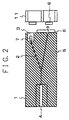
- Fig. 2 is a top view of the second embodiment of the optical waveguide module of the present invention.
- a function that is almost equivalent to the first embodiment has the same reference number that the first embodiment has.
- the disposition of each function is different from the first embodiment.
- an LD mounting area 3 and a waveguide coar part 9 and a V shaped groove for mounting an optical fiber 4 the surfaces being the upper surface covered with the waveguide clad 10, the bottom surface, and the side surfaces of the waveguide substrate 1 are covered with the metal deposition 5 or coated with the resin material.
- the stray light from the LD 7 is shut in the waveguide substrate 1 and the waveguide clad 10 and is not radiated to the outside of the waveguide substrate 1 and the waveguide clad 10. Further, the optical signals from the LD7 are not circulated to the PD 8 for receiving optical signals. Therefore, at the optical transceiver module in which transmitting and receiving optical signals are operated simultaneously, the conventional problem, which the receiving characteristic such as the receiving sensitivity is deteriorated caused by noise having a long time constant soon after the operation is changed to receiving, can be improved.
- an optical waveguide module provides a waveguide pattern, an LD mounting area, and a V shaped groove for mounting an optical fiber on a waveguide substrate, and further provides a waveguide core part from which light is radiated on the end surface of the waveguide substrate.
- the surfaces of the waveguide substrate and a waveguide clad are covered with a metal deposition having a characteristic that does not make stray light transmitting through a part not being the waveguide core part penetrate but makes the stray light reflect. And the stray light transmitting through a part not being the waveguide core part is shut in the waveguide substrate and the waveguide clad by the metal deposition.
- the stray light which circulates from an LD to a PD for receiving optical signals, can be shielded. Consequently, the receiving characteristic such as the receiving sensitivity, which is deteriorated by the stray light, can be improved.
Landscapes
- Physics & Mathematics (AREA)
- General Physics & Mathematics (AREA)
- Optics & Photonics (AREA)
- Optical Integrated Circuits (AREA)
- Optical Couplings Of Light Guides (AREA)
- Semiconductor Lasers (AREA)
- Light Receiving Elements (AREA)
Abstract
Description
Claims (10)
- A structure shielding stray light at an optical waveguide module, comprising:a waveguide pattern formed on a waveguide substrate;a laser diode (LD) mounting area formed on said waveguide substrate;a V shaped groove for mounting an optical fiber formed in said waveguide substrate;a waveguide clad formed on the upper surface of said waveguide substrate in which said waveguide pattern and said LD mounting area and said V shaped groove for mounting said optical fiber were formed;a waveguide core part, formed on the end surface of said waveguide clad, for radiating light; anda metal deposition, which covers the surfaces of said waveguide substrate and the surface of said waveguide clad except said waveguide core part and said LD mounting area and said V shaped groove for mounting said optical fiber, having a characteristic that does not make stray light transmitting through the other part of said waveguide core part penetrate and reflects said stray light, and shuts said stray light in said waveguide substrate and said waveguide clad.
- A structure shielding stray light at an optical waveguide module in accordance with claim 1, wherein:said metal deposition has a characteristic that does not make light of a wavelength band used in optical communication penetrate and reflects said light of said wavelength band used in said optical communication.
- A structure shielding stray light at an optical waveguide module in accordance with claim 1 or 2, wherein:said metal deposition is formed at least by any one of an evaporation method, a sputtering method, and a plating method.
- A structure shielding stray light at an optical waveguide module in accordance with claim 1, 2 or 3, wherein:said metal deposition is replaced with a resin coat which has a characteristic that does not make light having a wavelength band used in optical communication penetrate and reflects said light having said wavelength band used in said optical communication.
- A structure shielding stray light at an optical waveguide module in accordance with claim 1, 2 or 3, wherein:said metal deposition is replaced with a resin coat which has a characteristic that does not make light having a wavelength band used in optical communication penetrate and absorbs said light having said wavelength band used in said optical communication.
- An optical transceiver module unifying a transmitting function and a receiving function at optical communication, comprising:an optical waveguide module, providing:a waveguide pattern formed on a waveguide substrate;a LD mounting area formed on said waveguide substrate;a V shaped groove for mounting an optical fiber formed in said waveguide substrate;a waveguide clad formed on the upper surface of said waveguide substrate in which said waveguide pattern and said LD mounting area and said V shaped groove for mounting said optical fiber were formed;a waveguide core part, formed on the end surface of said waveguide clad, for radiating light; anda metal deposition, which covers the surfaces of said waveguide substrate and the surface of said waveguide clad except said waveguide core part and said LD mounting area and said V shaped groove for mounting said optical fiber, having a characteristic that does not make stray light transmitting through the other part of said waveguide core part penetrate and reflects said stray light, and shuts said stray light in said waveguide substrate and said waveguide clad.
- An optical transceiver module unifying a transmitting function and a receiving function at optical communication in accordance with claim 6, wherein:said metal deposition has a characteristic that does not make light of a wavelength band used in optical communication penetrate and reflects said light of said wavelength band used in said optical communication.
- An optical transceiver module unifying a transmitting function and a receiving function at optical communication in accordance with claim 6 or 7, wherein:said metal deposition is formed at least by any one of an evaporation method, a sputtering method, and a plating method.
- An optical transceiver module unifying a transmitting function and a receiving function at optical communication in accordance with claim 6, 7 or 8, wherein:said metal deposition is replaced with a resin coat which has a characteristic that does not make light having a wavelength band used in optical communication penetrate and reflects said light having said wavelength band used in said optical communication.
- An optical transceiver module unifying a transmitting function and a receiving function at optical communication in accordance with claim 6, 7 or 8, wherein:said metal deposition is replaced with a resin coat which has a characteristic that does not make light having a wavelength band used in optical communication penetrate and absorbs said light having said wavelength band used in said optical communication.
Applications Claiming Priority (2)
| Application Number | Priority Date | Filing Date | Title |
|---|---|---|---|
| JP31317099A JP2001133645A (en) | 1999-11-04 | 1999-11-04 | Stray light shielding structure for optical waveguide module and optical transmission/reception module using the same |
| JP31317099 | 1999-11-04 |
Publications (3)
| Publication Number | Publication Date |
|---|---|
| EP1098214A2 true EP1098214A2 (en) | 2001-05-09 |
| EP1098214A3 EP1098214A3 (en) | 2004-02-11 |
| EP1098214B1 EP1098214B1 (en) | 2007-04-11 |
Family
ID=18037961
Family Applications (1)
| Application Number | Title | Priority Date | Filing Date |
|---|---|---|---|
| EP00123442A Expired - Lifetime EP1098214B1 (en) | 1999-11-04 | 2000-11-03 | Optical waveguide module and optical transceiver with stray light shielding |
Country Status (4)
| Country | Link |
|---|---|
| US (1) | US6385375B1 (en) |
| EP (1) | EP1098214B1 (en) |
| JP (1) | JP2001133645A (en) |
| DE (1) | DE60034290T2 (en) |
Cited By (1)
| Publication number | Priority date | Publication date | Assignee | Title |
|---|---|---|---|---|
| EP2677355A3 (en) * | 2012-06-19 | 2015-06-03 | Nippon Telegraph And Telephone Corporation | Optical module |
Families Citing this family (11)
| Publication number | Priority date | Publication date | Assignee | Title |
|---|---|---|---|---|
| JP3879521B2 (en) * | 2001-04-23 | 2007-02-14 | オムロン株式会社 | Optical element and optical transceiver and other optical apparatus using the optical element |
| JP3885602B2 (en) | 2001-04-23 | 2007-02-21 | オムロン株式会社 | Optical element and optical transceiver and other optical apparatus using the optical element |
| US6944377B2 (en) | 2002-03-15 | 2005-09-13 | Hitachi Maxell, Ltd. | Optical communication device and laminated optical communication module |
| JP4253027B2 (en) * | 2006-11-21 | 2009-04-08 | 古河電気工業株式会社 | Optical module |
| WO2014156959A1 (en) * | 2013-03-25 | 2014-10-02 | 技術研究組合光電子融合基盤技術研究所 | Optical end coupling type silicon optical integrated circuit |
| JP6186654B2 (en) * | 2013-06-24 | 2017-08-30 | 華為技術有限公司Huawei Technologies Co.,Ltd. | Optical module and optical network system |
| WO2015008451A1 (en) * | 2013-07-18 | 2015-01-22 | 日本電気株式会社 | Optical transmission/reception module |
| JP6291278B2 (en) * | 2014-02-19 | 2018-03-14 | 株式会社エンプラス | Detection device |
| US9739938B2 (en) * | 2015-12-09 | 2017-08-22 | Elenion Technologies, Llc | Shielded photonic integrated circuit |
| JP7509597B2 (en) * | 2020-01-30 | 2024-07-02 | 株式会社キーエンス | Optical detection unit |
| JP2023167293A (en) * | 2022-05-11 | 2023-11-24 | 新光電気工業株式会社 | Silicon photonics element, optical module, and method for manufacturing optical module |
Family Cites Families (4)
| Publication number | Priority date | Publication date | Assignee | Title |
|---|---|---|---|---|
| FR2663435B1 (en) * | 1990-06-13 | 1992-09-11 | Commissariat Energie Atomique | INTEGRATED SINGLE - MODE SPACE OPTICAL FILTER AND MANUFACTURING METHOD THEREOF. |
| DE69620515T2 (en) * | 1995-07-26 | 2002-08-14 | Sumitomo Electric Industries, Ltd. | Photodiodes / diode laser module and photodiode module |
| US6480639B2 (en) * | 1997-09-26 | 2002-11-12 | Nippon Telegraph And Telephone Corp. | Optical module |
| JP3637228B2 (en) * | 1999-02-09 | 2005-04-13 | 住友電気工業株式会社 | Optical transceiver module |
-
1999
- 1999-11-04 JP JP31317099A patent/JP2001133645A/en active Pending
-
2000
- 2000-10-31 US US09/699,504 patent/US6385375B1/en not_active Expired - Lifetime
- 2000-11-03 EP EP00123442A patent/EP1098214B1/en not_active Expired - Lifetime
- 2000-11-03 DE DE60034290T patent/DE60034290T2/en not_active Expired - Lifetime
Cited By (1)
| Publication number | Priority date | Publication date | Assignee | Title |
|---|---|---|---|---|
| EP2677355A3 (en) * | 2012-06-19 | 2015-06-03 | Nippon Telegraph And Telephone Corporation | Optical module |
Also Published As
| Publication number | Publication date |
|---|---|
| US6385375B1 (en) | 2002-05-07 |
| EP1098214B1 (en) | 2007-04-11 |
| DE60034290D1 (en) | 2007-05-24 |
| JP2001133645A (en) | 2001-05-18 |
| EP1098214A3 (en) | 2004-02-11 |
| DE60034290T2 (en) | 2007-08-30 |
Similar Documents
| Publication | Publication Date | Title |
|---|---|---|
| US6546171B2 (en) | Structure for shielding stray light in optical waveguide module | |
| US6385375B1 (en) | Structure shielding stray light at optical waveguide module and optical transceiver module used this structure | |
| EP0905536B1 (en) | Optical module | |
| US6547451B1 (en) | Optical communications module and method for mounting optical communications module | |
| US20020031307A1 (en) | Optical communication module and process for producing the same | |
| US6853776B2 (en) | Optical communication module and manufacturing method thereof | |
| JPH1168705A (en) | Bidirectional WDM optical transceiver module | |
| US20090196617A1 (en) | Single core bidirectional optical device | |
| JP2003098397A (en) | Bidirectional optical transmission device | |
| US20030086653A1 (en) | Sub-mount and optical receiver using the same | |
| EP0733288B1 (en) | Optoelectronic semiconductor device comprising laser and photodiode | |
| US20010002942A1 (en) | Optical transmission and reception module using optical waveguide | |
| US6634803B2 (en) | External EMI shield for multiple array optoelectronic devices | |
| JP3767842B2 (en) | Bi-directional optical communication module | |
| JP3557966B2 (en) | Optical communication module with light blocking filter | |
| JP2001174675A (en) | Optical waveguide type module | |
| US5933553A (en) | Arrangement for transmitting and receiving optical signals | |
| US20040026604A1 (en) | Optical transceiver | |
| US6520652B1 (en) | Method and apparatus for reducing undesirable reflected light in integrated opto-electronic modules | |
| JPH11287932A (en) | Optical module | |
| WO2023162182A1 (en) | Optical receiver | |
| US6527454B1 (en) | Optical module for receiving and transmitting light signal in optical communication | |
| US20060110094A1 (en) | Bidirectional electro-optical device for coupling light-signals into and out of a waveguide | |
| CN115079347B (en) | Light emitting and receiving component and optical path coupling method for light emitting and receiving component | |
| HK40057990A (en) | Optical module |
Legal Events
| Date | Code | Title | Description |
|---|---|---|---|
| PUAI | Public reference made under article 153(3) epc to a published international application that has entered the european phase |
Free format text: ORIGINAL CODE: 0009012 |
|
| AK | Designated contracting states |
Kind code of ref document: A2 Designated state(s): AT BE CH CY DE DK ES FI FR GB GR IE IT LI LU MC NL PT SE TR |
|
| AX | Request for extension of the european patent |
Free format text: AL;LT;LV;MK;RO;SI |
|
| PUAL | Search report despatched |
Free format text: ORIGINAL CODE: 0009013 |
|
| AK | Designated contracting states |
Kind code of ref document: A3 Designated state(s): AT BE CH CY DE DK ES FI FR GB GR IE IT LI LU MC NL PT SE TR |
|
| AX | Request for extension of the european patent |
Extension state: AL LT LV MK RO SI |
|
| 17P | Request for examination filed |
Effective date: 20040105 |
|
| 17Q | First examination report despatched |
Effective date: 20040428 |
|
| AKX | Designation fees paid |
Designated state(s): DE GB |
|
| GRAP | Despatch of communication of intention to grant a patent |
Free format text: ORIGINAL CODE: EPIDOSNIGR1 |
|
| GRAS | Grant fee paid |
Free format text: ORIGINAL CODE: EPIDOSNIGR3 |
|
| GRAA | (expected) grant |
Free format text: ORIGINAL CODE: 0009210 |
|
| AK | Designated contracting states |
Kind code of ref document: B1 Designated state(s): DE GB |
|
| REG | Reference to a national code |
Ref country code: GB Ref legal event code: FG4D |
|
| REF | Corresponds to: |
Ref document number: 60034290 Country of ref document: DE Date of ref document: 20070524 Kind code of ref document: P |
|
| PLBE | No opposition filed within time limit |
Free format text: ORIGINAL CODE: 0009261 |
|
| STAA | Information on the status of an ep patent application or granted ep patent |
Free format text: STATUS: NO OPPOSITION FILED WITHIN TIME LIMIT |
|
| 26N | No opposition filed |
Effective date: 20080114 |
|
| PGFP | Annual fee paid to national office [announced via postgrant information from national office to epo] |
Ref country code: DE Payment date: 20101027 Year of fee payment: 11 |
|
| PGFP | Annual fee paid to national office [announced via postgrant information from national office to epo] |
Ref country code: GB Payment date: 20101103 Year of fee payment: 11 |
|
| GBPC | Gb: european patent ceased through non-payment of renewal fee |
Effective date: 20121103 |
|
| REG | Reference to a national code |
Ref country code: DE Ref legal event code: R119 Ref document number: 60034290 Country of ref document: DE Effective date: 20130601 |
|
| PG25 | Lapsed in a contracting state [announced via postgrant information from national office to epo] |
Ref country code: DE Free format text: LAPSE BECAUSE OF NON-PAYMENT OF DUE FEES Effective date: 20130601 |
|
| PG25 | Lapsed in a contracting state [announced via postgrant information from national office to epo] |
Ref country code: GB Free format text: LAPSE BECAUSE OF NON-PAYMENT OF DUE FEES Effective date: 20121103 |