EP1098203A2 - Magnetic tunnel junction element, tunneling magnetoresistive head, and production methods - Google Patents
Magnetic tunnel junction element, tunneling magnetoresistive head, and production methods Download PDFInfo
- Publication number
- EP1098203A2 EP1098203A2 EP00123750A EP00123750A EP1098203A2 EP 1098203 A2 EP1098203 A2 EP 1098203A2 EP 00123750 A EP00123750 A EP 00123750A EP 00123750 A EP00123750 A EP 00123750A EP 1098203 A2 EP1098203 A2 EP 1098203A2
- Authority
- EP
- European Patent Office
- Prior art keywords
- magnetic
- layer
- film
- tunnel junction
- junction element
- Prior art date
- Legal status (The legal status is an assumption and is not a legal conclusion. Google has not performed a legal analysis and makes no representation as to the accuracy of the status listed.)
- Withdrawn
Links
Images


Classifications
-
- B—PERFORMING OPERATIONS; TRANSPORTING
- B82—NANOTECHNOLOGY
- B82Y—SPECIFIC USES OR APPLICATIONS OF NANOSTRUCTURES; MEASUREMENT OR ANALYSIS OF NANOSTRUCTURES; MANUFACTURE OR TREATMENT OF NANOSTRUCTURES
- B82Y25/00—Nanomagnetism, e.g. magnetoimpedance, anisotropic magnetoresistance, giant magnetoresistance or tunneling magnetoresistance
-
- B—PERFORMING OPERATIONS; TRANSPORTING
- B82—NANOTECHNOLOGY
- B82Y—SPECIFIC USES OR APPLICATIONS OF NANOSTRUCTURES; MEASUREMENT OR ANALYSIS OF NANOSTRUCTURES; MANUFACTURE OR TREATMENT OF NANOSTRUCTURES
- B82Y10/00—Nanotechnology for information processing, storage or transmission, e.g. quantum computing or single electron logic
-
- G—PHYSICS
- G01—MEASURING; TESTING
- G01R—MEASURING ELECTRIC VARIABLES; MEASURING MAGNETIC VARIABLES
- G01R33/00—Arrangements or instruments for measuring magnetic variables
- G01R33/02—Measuring direction or magnitude of magnetic fields or magnetic flux
- G01R33/06—Measuring direction or magnitude of magnetic fields or magnetic flux using galvano-magnetic devices
- G01R33/09—Magnetoresistive devices
- G01R33/093—Magnetoresistive devices using multilayer structures, e.g. giant magnetoresistance sensors
-
- G—PHYSICS
- G01—MEASURING; TESTING
- G01R—MEASURING ELECTRIC VARIABLES; MEASURING MAGNETIC VARIABLES
- G01R33/00—Arrangements or instruments for measuring magnetic variables
- G01R33/02—Measuring direction or magnitude of magnetic fields or magnetic flux
- G01R33/06—Measuring direction or magnitude of magnetic fields or magnetic flux using galvano-magnetic devices
- G01R33/09—Magnetoresistive devices
- G01R33/098—Magnetoresistive devices comprising tunnel junctions, e.g. tunnel magnetoresistance sensors
-
- G—PHYSICS
- G11—INFORMATION STORAGE
- G11B—INFORMATION STORAGE BASED ON RELATIVE MOVEMENT BETWEEN RECORD CARRIER AND TRANSDUCER
- G11B5/00—Recording by magnetisation or demagnetisation of a record carrier; Reproducing by magnetic means; Record carriers therefor
- G11B5/127—Structure or manufacture of heads, e.g. inductive
- G11B5/33—Structure or manufacture of flux-sensitive heads, i.e. for reproduction only; Combination of such heads with means for recording or erasing only
- G11B5/39—Structure or manufacture of flux-sensitive heads, i.e. for reproduction only; Combination of such heads with means for recording or erasing only using magneto-resistive devices or effects
- G11B5/3903—Structure or manufacture of flux-sensitive heads, i.e. for reproduction only; Combination of such heads with means for recording or erasing only using magneto-resistive devices or effects using magnetic thin film layers or their effects, the films being part of integrated structures
- G11B5/3906—Details related to the use of magnetic thin film layers or to their effects
- G11B5/3909—Arrangements using a magnetic tunnel junction
-
- H—ELECTRICITY
- H01—ELECTRIC ELEMENTS
- H01F—MAGNETS; INDUCTANCES; TRANSFORMERS; SELECTION OF MATERIALS FOR THEIR MAGNETIC PROPERTIES
- H01F10/00—Thin magnetic films, e.g. of one-domain structure
- H01F10/32—Spin-exchange-coupled multilayers, e.g. nanostructured superlattices
- H01F10/324—Exchange coupling of magnetic film pairs via a very thin non-magnetic spacer, e.g. by exchange with conduction electrons of the spacer
- H01F10/3254—Exchange coupling of magnetic film pairs via a very thin non-magnetic spacer, e.g. by exchange with conduction electrons of the spacer the spacer being semiconducting or insulating, e.g. for spin tunnel junction [STJ]
-
- H—ELECTRICITY
- H01—ELECTRIC ELEMENTS
- H01F—MAGNETS; INDUCTANCES; TRANSFORMERS; SELECTION OF MATERIALS FOR THEIR MAGNETIC PROPERTIES
- H01F10/00—Thin magnetic films, e.g. of one-domain structure
- H01F10/32—Spin-exchange-coupled multilayers, e.g. nanostructured superlattices
- H01F10/324—Exchange coupling of magnetic film pairs via a very thin non-magnetic spacer, e.g. by exchange with conduction electrons of the spacer
- H01F10/3268—Exchange coupling of magnetic film pairs via a very thin non-magnetic spacer, e.g. by exchange with conduction electrons of the spacer the exchange coupling being asymmetric, e.g. by use of additional pinning, by using antiferromagnetic or ferromagnetic coupling interface, i.e. so-called spin-valve [SV] structure, e.g. NiFe/Cu/NiFe/FeMn
-
- H—ELECTRICITY
- H10—SEMICONDUCTOR DEVICES; ELECTRIC SOLID-STATE DEVICES NOT OTHERWISE PROVIDED FOR
- H10N—ELECTRIC SOLID-STATE DEVICES NOT OTHERWISE PROVIDED FOR
- H10N50/00—Galvanomagnetic devices
- H10N50/01—Manufacture or treatment
-
- H—ELECTRICITY
- H10—SEMICONDUCTOR DEVICES; ELECTRIC SOLID-STATE DEVICES NOT OTHERWISE PROVIDED FOR
- H10N—ELECTRIC SOLID-STATE DEVICES NOT OTHERWISE PROVIDED FOR
- H10N50/00—Galvanomagnetic devices
- H10N50/10—Magnetoresistive devices
-
- G—PHYSICS
- G11—INFORMATION STORAGE
- G11B—INFORMATION STORAGE BASED ON RELATIVE MOVEMENT BETWEEN RECORD CARRIER AND TRANSDUCER
- G11B5/00—Recording by magnetisation or demagnetisation of a record carrier; Reproducing by magnetic means; Record carriers therefor
- G11B5/127—Structure or manufacture of heads, e.g. inductive
- G11B5/33—Structure or manufacture of flux-sensitive heads, i.e. for reproduction only; Combination of such heads with means for recording or erasing only
- G11B5/39—Structure or manufacture of flux-sensitive heads, i.e. for reproduction only; Combination of such heads with means for recording or erasing only using magneto-resistive devices or effects
- G11B2005/3996—Structure or manufacture of flux-sensitive heads, i.e. for reproduction only; Combination of such heads with means for recording or erasing only using magneto-resistive devices or effects large or giant magnetoresistive effects [GMR], e.g. as generated in spin-valve [SV] devices
Definitions
- the present invention relates to a magnetic tunnel junction element including a pair of magnetic layers formed via an insulation layer in which conductance of tunnel current flowing from one of the magnetic layers to the other magnetic layer varies depending on a relative angle of magnetization of the pair of magnetic layers and a production method of the magnetic tunnel junction element. Moreover, the present invention relates to a tunneling magnetoresistive head having such a magnetic tunnel junction element and a production method thereof.
- a so-called magnetic tunnel effect has been reported conventionally.
- a so-called tunnel current flows via the insulation layer and the conductance of the tunnel current varies depending on a relative angle of magnetization of the pair of magnetic layers. That is, in a layered configuration having a thin insulation layer sandwiched by a pair of magnetic layers, the magnetoresistive effect is observed against the tunnel current flowing in the insulation layer.
- the magnetoresistance ratio can be theoretically calculated from the polarization ratio of the magnetization of the pair of magnetic layers. Especially, when Fe is employed as the material of the pair of the magnetic layers, a magnetoresistance ratio of about 40 % can be expected.
- a magnetic tunnel junction element having a layered configuration of a thin insulation layer sandwiched by a pair of magnetic layers is now gathering attention as a magnetoresistive element.
- Special attention is now paid in the field of magnetic heads, on a so-called tunneling magnetoresistive head (hereinafter, referred to as a TMR head) in which the magnetic tunnel junction element is used as a magnet sensitive element for detecting a magnetic signal from a magnetic recording medium.
- TMR head tunneling magnetoresistive head
- a magnetic domain control is required for suppressing the Barkhausen noise.
- a pair of bias layers are provided so as to be connected electrically and magnetically to the both sides of the magnetoresistive element.
- the magnetic tunnel junction element includes: a first magnetic layer having magnetization fixed in a predetermined direction, an insulation layer formed on the first magnetic layer, and a second magnetic layer formed on the insulation layer and changing its magnetization direction according to an external magnetic field, wherein the second magnetic layer is provided with non-conducting magnetic domain control films formed at both end portions on the second magnetic layer.
- non-conducting magnetic domain control films are formed at both end portions of the second magnetic layers. Accordingly, it is possible to perform magnetic domain control of the second magnetic layer without causing any electric short circuit and to suppress generation of Barkhausen noise.
- the magnetic tunnel junction element production method includes steps of: forming a first magnetic layer having its magnetization direction fixed in a predetermined direction, forming an insulation layer on the first magnetic layer, forming a second magnetic layer on the insulation layer so as to change its magnetization direction according to an external magnetic field, forming a non-conducting magnetic domain control film on the second magnetic layer, forming a resist pattern having a predetermined configuration on the magnetic domain control film, and removing the magnetic domain control film by etching using the resist pattern excluding the both end portions on the second magnetic layer.
- the magnetic tunnel junction element production method it is possible to successively form at least first magnetic layer, an insulation layer, a second magnetic layer, and a magnetic domain control film in this order in a single apparatus.
- the tunneling magnetoresistive head includes a first magnetic layer having magnetization fixed in a predetermined direction, an insulation layer formed on the first magnetic layer, a second magnetic layer formed on the insulation layer and changing its magnetization direction according to an external magnetic field, wherein the second magnetic layer is provided with non-conducting magnetic domain control films on both end portions thereof.
- non-conducting magnetic domain control films are formed on both end portions on the second magnetic layer of the magnetic tunnel junction element. Accordingly, it is possible to perform the magnetic domain control of the second magnetic layer without causing any electric short circuit and to suppress Barkhausen noise.
- the tunneling magnetoresistive head production method including a magnetic tunnel junction element is produced by steps of: forming a first magnetic layer having its magnetization direction fixed in a predetermined direction, forming an insulation layer on the first magnetic layer, forming a second magnetic layer on the insulation layer so as to change its magnetization direction according to an external magnetic field, forming a non-conducting magnetic domain control film on the second magnetic layer, forming a resist pattern having a predetermined configuration on the magnetic domain control film, and removing the magnetic domain control film by etching using the resist pattern excluding the both end portions on the second magnetic layer.
- the tunneling magnetoresistive head production method it is possible to successively form at least the first magnetic layer, the insulation layer, the second magnetic layer, and the magnetic domain control film in this order in a single apparatus so as to constitute the magnetic tunnel junction element.
- the magnetic tunnel junction element has a layered configuration of a first magnetic metal layer 1 and a second magnetic metal layer 2 which are layered via a tunnel barrier layer 3.
- a first electrode 4a and a second electrode 4b are connected to the first magnetic metal layer 1 and the second magnetic metal layer 2, respectively.
- Fig. 2 shows an enlarged perspective view of the portion in the magnetic tunnel junction element where the first magnetic metal layer 1 and the second magnetic metal layer 2 are layered via the tunnel barrier layer 3.
- the first magnetic metal layer 1 has a magnetization-fixed layer not changing its magnetization direction with respect to an external magnetic field. More specifically, the first magnetic metal layer 1 has a two-layered configuration having, for example, an IrMn film 5 and a CoFe film 6 successively layered from the side of the first electrode 4a.
- the IrMn film 5 is made from an antiferromagnetic material and exchange coupling with the CoFe film 6 and fixes the magnetization of the CoFe film 6 in a predetermined direction. That is, in this magnetic tunnel junction element, the CoFe film 6 is a magnetization-fixed layer having a fixed magnetization in a predetermined direction.
- the second magnetic metal layer 2 has a magnetization free layer changing its magnetization direction according to an external magnetic field. More specifically, the second magnetic metal layer 2 has a two-layered configuration of a CoFe film 7 and a NiFe film 8 which are successively layered from the side of the tunnel barrier layer 3.
- the CoFe film 7 serves to increase the spin polarizability while the NiFe film 8 has a low coercive force and serves as a magnetization free layer changing its magnetization direction according to an external magnetic field.
- the second magnetic metal layer 2 having such a two-layered configuration can increase the magnetoresistance ratio of the magnetic tunnel junction element.
- the tunnel barrier layer 3 is formed from an insulation material such as Al 2 O 3 .
- a non-conductive magnetic domain control film 9 is arranged at both end portions of the second magnetic metal layer 2.
- the magnetic domain control film 9 is formed from a non-conductive antiferromagnetic material or a ferromagnetic material such as NiO.
- the NiO is a non-conductive oxide-system antiferromagnetic material and exchange coupling with the NiFe film 8 (magnetization free layer), performing a magnetic domain control of the NiFe film 8.
- a portion of the NiFe film 8 (magnetization free layer) sandwiched by the magnetic domain control films 9 serves as a magnet sensitive portion of the magnetic tunnel junction element.
- This magnetic tunnel junction element is produced by a thin film formation step and the components constituting the magnetic tunnel junction element are successively layered on the basic material 10. That is, the magnetic tunnel junction element includes the first electrode 4a. the first magnetic metal layer 1, the tunnel barrier layer 3, and the second magnetic metal layer 2 which are successively layered on the basic material 10, and the magnetic domain control film 9 is formed at both end portions of the second magnetic metal layer 2, and the second electrode 4b is formed thereon.
- the basic material 10 includes, for example, an insulation layer of SiO 2 , formed on a substrate 11 having smoothing surface made from Si.
- the IrMn film 5 is formed with a film thickness of about 10 nm and the CoFe film 6 is formed with a film thickness of about 5 nm.
- the IrMn film 5 and the CoFe film 6 are successively formed by sputtering or the like.
- the tunnel barrier layer 3 is formed by an Al 2 O 3 film with a film thickness of about 1.3 nm.
- This Al 2 O 3 film may be formed by forming an Al film on the CoFe film 6 by sputtering and oxidizing the film into Al 2 O 3 using an oxygen plasma or the like, or by directly forming an Al 2 O 3 film on the CoFe film 7 using the sputtering or the like.
- the tunnel barrier layer 3 is not to be limited to the Al 2 O 3 film but may be made from any insulation material if it serves as a tunnel barrier of the so-called tunnel current, i.e., current flowing between the first magnetic metal layer 1 and the second magnetic metal layer 2.
- the CoFe film 7 is formed with a film thickness of about 5 nm while the NiFe film 8 is formed with a film thickness of about 20 nm.
- the CoFe film 7 and the NiFe film 8 are successively formed by sputtering or the like.
- the magnetic domain control film 9 is formed by a NiO film with a film thickness of about 50 nm.
- the magnetic domain control film 9 is not to be limited to the NiO film but may be formed from any non-conductive antiferromagnetic material or non-conductive hard magnetic material if it can perform the magnetic domain control of the NiFe film 8.
- the magnetic tunnel junction element When producing the magnetic tunnel junction element, it is possible to successively form the IrMn film 5, the CoFe film 6 (magnetization-fixed layer), the Al 2 O 3 film (tunnel barrier layer 3), the CoFe film 7, the NiFe film 8 (magnetization free layer), and the NiO film (magnetic domain control film 9) by sputtering or the like. These films can be successively formed with the same chamber without exposing the film materials to the atmosphere.
- the IrMn film 5, the CoFe film 6, the Al 2 O 3 film, the CoFe film 7, the NiFe film, and the NiO film are successively formed in the same chamber by sputtering or the like.
- a resist material is applied onto the NiO film to form a resist film.
- This resist film is patterned into a predetermined pattern using the photolithography technique so as to obtain a resist pattern.
- the resist pattern is formed by patterning which leaves the resist film at portions other than the magnet sensitive portion of the magnetic tunnel junction element.
- this resist pattern is used as a mask when performing ion etching to remove the portion of the NiO film to serve as the magnet sensitive portion, so that the NiO film is formed at both end portions of the NiFe film 8.
- the magnetic tunnel junction element when producing the magnetic tunnel junction element, it is possible to successively form the components of the magnetic tunnel junction element in a single chamber without exposing them to the atmosphere. Accordingly, the magnetic tunnel junction element can be prepared with a high accuracy.
- a tunnel current flows via the tunnel barrier layer 3 in the direction indicated by arrow A in Fig. 1, i.e., in the direction from the second magnetic metal layer 2 to the first magnetic metal layer 1.
- the CoFe film 6 of the first magnetic metal layer 1 serves as the magnetization-fixed layer not changing its magnetization direction while the NiFe film 8 of the second magnetic metal layer 2 serves as the magnetization free layer changing its magnetization direction according to an external magnetic field.
- the CoFe film 6 (magnetization-fixed layer) is exchange coupling with the IrMn film 5 as the antiferromagnetic material and has a magnetization direction fixed in the direction indicated by arrow B in Fig. 2.
- the NiFe film 8 (magnetization free layer) is formed so as to have a uniaxial anisotropy in the direction indicated by arrow C in Fig. 2. Accordingly, when no external magnetic field is applied, the CoFe film 6 has a magnetization direction which approximately orthogonally intersects the magnetization direction of the NiFe film 8.
- the NiFe film 8 (magnetization free layer) is exchange coupling with the magnetic domain control film 9 (NiO film) formed thereon and has its magnetization direction fixed in the direction indicated by arrow C in Fig. 2. That is, the NiFe film 8 is controlled by the magnetic domain control film 9 formed at both end portions of the NiFe film 8, so that it has a single magnetic domain in the direction identical to the direction of the uniaxial anisotropy of the NiFe film 8. Accordingly, in this magnetic tunnel junction element, it is possible to suppress the Barkhausen noise generated by a discontinuous movement of a magnetic domain of the NiFe film 8 (magnetization free layer).
- the tunnel current flows only into the magnet sensitive portion sandwiched by the magnetic domain control films 9.
- the magnetization direction of the NiFe film 8 (magnetization free layer) is changed to define a predetermined angle with the magnetization direction of the CoFe film 6 (magnetization-fixed layer).
- the resistance against the tunnel current changes depending on the relative angle between defined by the magnetization free layer and the magnetization-fixed layer. Accordingly, in this magnetic tunnel junction element, the external magnetic field change can be detected by measuring the resistance value change.
- the magnetic domain control film 9 NiO film having non-conductance is arranged at both end portions of the NiFe film 8 (magnetization free layer) so that the magnetic domain control of the NiFe film 8 is performed by the magnetic domain control films 9.
- the magnetic tunnel junction element there is no danger of electrical short circuit and the current can be made to flow only in the magnet sensitive portion of the NiFe film 8 (magnetization free layer). Accordingly, it is possible to suppress the Barkhausen noise generated by a discontinuous movement of a magnetic domain of the NiFe film 8 and to obtain a preferable characteristic.
- TMR head tunneling magnetoresistive head
- this TMR head includes a magnetic tunnel junction element 20 sandwiched by a lower shield layer 21 and an upper shield layer 22 via a lower gap layer 23 and an upper gap layer 24.
- the magnetic tunnel junction element 20 is the aforementioned magnetic tunnel junction element according to the present invention applied to a magnetic head and includes a first magnetic metal layer 25 and a second magnetic metal layer 26 which are layered via a tunnel barrier layer 27.
- the first magnetic metal layer 25 has a magnetization-fixed layer which does not change its magnetization direction with respect to an external magnetic field. More specifically, the first magnetic metal layer 25, for example, has a two-layered configuration including an IrMn film 28 and a CoFe film 29 which are successively layered from the side of the lower gap layer 23.
- the IrMn film 28 is an antiferromagnetic material and exchange coupling with the CoFe film 29, so that the magnetization direction of the CoFe film 29 is fixed in a predetermined direction. That is, in this magnetic tunnel junction element 20, the CoFe film 29 serves as a magnetization-fixed layer having a fixed magnetization in a predetermined direction.
- the second magnetic metal layer 26 has a magnetization free layer which changes its magnetization direction according to an external magnetic field. More specifically, the second magnetic metal layer 26, for example, has a two-layered configuration including a CoFe film 30 and a NiFe film 31 which are successively layered from the side of the tunnel barrier layer 27.
- the CoFe film 30 is used to increase the spin polarizability while the NiFe film 31 has a low coercive force and serves as a magnetization free layer changing its magnetization direction according to an external magnetic field.
- the second magnetic metal layer 26 having such a two-layered configuration can increase the magnetic resistance ratio of the magnetic tunnel junction element 20.
- the tunnel barrier layer 27 is formed, for example, from an insulation material such as Al 2 O 3 .
- the magnetic tunnel junction element 20 includes a non-conducting magnetic domain control film 32 arranged at both end portions of the medium facing sides on the NiFe film 31 (magnetization free layer).
- This magnetic domain control film 32 is made from a non-conducting antiferromagnetic material or ferromagnetic material such as NiO.
- the NiO is a non-conducting oxide-system antiferromagnetic material exchange coupling with the NiFe film 31 and performs a magnetic domain control of the NiFe film 31.
- one end surface exposed externally is the medium facing surface to face a magnetic recording medium and the portion sandwiched by the NiFe film 31 and the magnetic domain control film 32 in the magnetic tunnel junction element 20 serves as a magnet sensitive portion of the magnetic tunnel junction element 20.
- the upper shield layer 22 and the lower shield layer 21 are made from a magnetic material having electric conductivity.
- the upper gap layer 24 and the lower gap layer 23 is made from a non-magnetic material having electric conductivity.
- the first magnetic metal layer 25 is magnetically isolated from the lower shield layer 21, and the second magnetic metal layer 26 is also magnetically isolated from the upper shield layer 22.
- the lower shield layer 21, the lower gap layer 23, the upper gap layer 24, and the upper shield layer 22 are made from a material having electric conductivity, the lower shield layer 21 and the lower gap layer 23 serve as an electrode with respect to the first magnetic metal layer 25 while the upper shield layer 22 and the upper gap layer 24 serve as an electrode with respect to the second magnetic metal layer 26.
- the TMR head is produced by a thin film formation step which will be detailed later and the components constituting this TMR head are successively layered on the substrate 33.
- this TMR head includes an insulation material filled in a space defined between the substrate 33 and the upper shield layer 22. More specifically, in the TMR head, the lower gap layer 23, the magnetic tunnel junction element 20, the magnetic domain control film 32, and the upper gap layer 24 are formed so as to be buried in the insulation material. Moreover, on the end portion of the lower shield layer 21, there is arranged a connection terminal 34 formed from a conductive material and having a height reaching the upper shield layer 22.
- the insulation material filled in the TMR head is omitted in the figure.
- the magnetization direction of the NiFe film 31 changes with respect to the CoFe film 29 (magnetization-fixed layer) having a magnetic domain fixed in a predetermined direction.
- a predetermined voltage is applied between the lower shield layer 21 and the upper shield layer 22 and a tunnel current is flowing from the second magnetic metal layer 26 to the first magnetic metal layer 25 via the tunnel barrier layer 27.
- the resistance value with respect to the tunnel current is changed.
- the non-conducting magnetic domain control film 32 is arranged at both end portions of the medium facing side on the NiFe film 31 (magnetization free layer) and this magnetic domain control film 32 performs the magnetic domain control of the NiFe film 31.
- an AlTiC-system or TiO-CaO-system substrate 33 is prepared as such that is usually used for producing a thin film type magnetic head.
- a magnetic metal film 35 is formed from sendust or the like to serve as the lower shield layer 21 and then a non-magnetic metal film 36 is formed from Ta or the like to serve as the lower gap layer 23.
- the non-magnetic metal film 36 is used as the undercoat layer of the magnetic tunnel junction element 20 and preferably has a highly flattened surface.
- an IrMn film 28 and a CoFe film 29 are successively formed to serve as the first magnetic metal layer 25.
- the IrMn film 28 is subjected to an orientation processing so that it is exchange coupling with the CoFe film 29 in an approximately parallel direction with respect to a signal magnetic field applied from a magnetic recording medium.
- a Al 2 O 3 film 37 is formed to serve as the tunnel barrier layer 27.
- This Al 2 O 3 film 37 is formed by forming an Al film on the CoFe film 29 and then oxidizing the Al film by oxygen plasma.
- the Al 2 O 3 film 37 is controlled in oxidization by adjusting, for example, the oxidization time, the gas pressure, the oxygen partial pressure, the high frequency power, and the like.
- the Al 2 O 3 film 37 may be formed by directly forming the Al 2 O 3 film on the CoFe film by sputtering.
- a CoFe film 30 and a NiFe film 31 are successively formed to serve as the second magnetic metal layer 26. Moreover, the CoFe film 30 and the NiFe film 31 are subjected to an orientation processing so as to have a uniaxial anisotropy in a direction approximately vertical to a signal magnetic field applied from a magnetic recording medium.
- an NiO film 38 is formed to serve as the magnetic domain control film 32.
- the NiO film 38 is subjected to an orientation processing so as to be exchange coupling with the NiFe film 31 in a direction approximately vertical to a signal magnetic field applied from a magnetic recording medium.
- a resist material is applied onto the NiO film 38 to form a resist film, which is patterned into a predetermined configuration using the photolithographic technique, so as to obtain a resist pattern 39. More specifically, the resist pattern 39 is formed by such a patterning that the resist film remains on a region other than the portion to become the magnet sensitive portion on the NiFe film 31.
- the NiO film 38 if the region not having the resist pattern 39 is etched and removed by the ion milling method or the like until the NiFe film 31 formed thereunder is exposed.
- the NiO film 38 and the resist pattern 39 remain on the region outside the magnet sensitive portion on the NiFe film 31.
- a non-magnetic metal film 40 such as Ta is formed by sputtering so as to serve as the upper gap layer 24.
- the non-magnetic metal film 40 remaining on the resist pattern 39 is peeled off and removed using an organic solvent or the like.
- the upper gap layer 24 is formed on the region to serve as the magnet sensitive portion on the NiFe film 31.
- a resist material is applied onto the upper gap layer 24 and the NiO film 38 so as to form a resist film, which is patterned into a predetermined configuration using the photolithographic technique so as to obtain a resist pattern 41. More specifically, the resist pattern 41 is formed by such a patterning that the resist pattern 41 remains on the region to become the magnetic tunnel junction element 20.
- the portion not having the resist pattern 41 is etched and removed by the ion milling method or the like until the magnetic metal film 35 formed thereunder is exposed to serve as the lower shield layer 21.
- the lower shield layer 21 having a predetermined configuration, the first magnetic metal layer 25, the tunnel barrier layer 27, the second magnetic metal layer 26, the magnetic domain control film 32, and the upper gap layer 24 are formed. That is, the magnetic tunnel junction element 20 having a predetermined configuration defined by the resist pattern 41.
- an insulation film 42 is formed by sputtering or the like so as to have almost identical height as the boundary between the resist pattern 41 and the magnetic domain control film 32 and the upper gap layer 24.
- the insulation film 42 remaining on the resist pattern 41 is peeled off and removed together with the resist pattern 41 using an organic solvent or the like.
- the magnetic tunnel junction element 20 is arranged as being buried in the insulation film 42.
- the upper shield layer 22 having a predetermined configuration is formed on the main surface from which the resist pattern 41 has been removed.
- the upper shield layer 22 may be formed by plating using a resist pattern having a predetermined configuration applied to the magnetic metal film to become the upper shield layer 22, or forming the magnetic metal film to become the upper shield layer 22 by sputtering and then etching it into a predetermined configuration.
- Photolithography and etching are used to form the insulation film 42 and the lower shield layer 21 into a predetermined configuration. Moreover, an opening is formed in the insulation film 42 on the end portion of the lower shield layer 21, so as to expose the lower shield layer 21. This opening is filled with a conducting material and a connection terminal 34 is formed on the lower shield layer 21. Thus, the lower shield layer 21 can be electrically connected together with the upper shield layer 22.
- the tunneling magnetoresistive head as shown in Fig. 3 is prepared.
- the magnetic tunnel junction element according to the present invention having the non-conducting magnetic domain control film formed at both end portions of the medium facing side of the second magnetic layer can suppress generation of the Barkhausen noise without causing an electric short circuit and obtain a preferable characteristic.
- the components of the magnetic tunnel junction element can be successively formed in a single apparatus without exposing them to the atmosphere, thereby enabling to prepare the magnetic tunnel junction element with a high accuracy.
- the non-conducting magnetic domain control film is formed at both end portions of the medium facing side of the second magnetic layer of the magnetic tunnel junction element and accordingly, no electric short circuit is generated.
- it is possible to suppress generation of the Barkhausen noise and stabilize the reproduction output.
- the tunneling magnetoresistive head production method it is possible to successively form the components of the tunneling magnetoresistive head in a single apparatus without exposing the components to the atmosphere. Thus, it is possible to prepare the tunneling magnetoresistive head with a high accuracy.
Abstract
The present invention suppresses generation of the Barkhausen noise by
providing a magnetic tunnel junction element including: a first magnetic layer having
magnetization fixed in a predetermined direction, an insulation layer formed on the
first magnetic layer, and a second magnetic layer formed on the insulation layer and
changing its magnetization direction according to an external magnetic field, wherein
the second magnetic layer is provided with non-conducting magnetic domain control
films formed at both end portions on the second magnetic layer.
Description
- The present invention relates to a magnetic tunnel junction element including a pair of magnetic layers formed via an insulation layer in which conductance of tunnel current flowing from one of the magnetic layers to the other magnetic layer varies depending on a relative angle of magnetization of the pair of magnetic layers and a production method of the magnetic tunnel junction element. Moreover, the present invention relates to a tunneling magnetoresistive head having such a magnetic tunnel junction element and a production method thereof.
- A so-called magnetic tunnel effect has been reported conventionally. In a layered configuration having a thin insulation layer sandwiched by a pair of magnetic layers, when a predetermined voltage is applied between the magnetic layers, a so-called tunnel current flows via the insulation layer and the conductance of the tunnel current varies depending on a relative angle of magnetization of the pair of magnetic layers. That is, in a layered configuration having a thin insulation layer sandwiched by a pair of magnetic layers, the magnetoresistive effect is observed against the tunnel current flowing in the insulation layer.
- In this magnetic tunnel effect, the magnetoresistance ratio can be theoretically calculated from the polarization ratio of the magnetization of the pair of magnetic layers. Especially, when Fe is employed as the material of the pair of the magnetic layers, a magnetoresistance ratio of about 40 % can be expected.
- For this, a magnetic tunnel junction element having a layered configuration of a thin insulation layer sandwiched by a pair of magnetic layers is now gathering attention as a magnetoresistive element. Special attention is now paid in the field of magnetic heads, on a so-called tunneling magnetoresistive head (hereinafter, referred to as a TMR head) in which the magnetic tunnel junction element is used as a magnet sensitive element for detecting a magnetic signal from a magnetic recording medium.
- In the aforementioned TMR head, like the magnetoresistive head (hereinafter, referred to as an MR head), a magnetic domain control is required for suppressing the Barkhausen noise. Generally, in the MR head, in order suppress this Barkhausen noise, a pair of bias layers are provided so as to be connected electrically and magnetically to the both sides of the magnetoresistive element.
- However, in the case of TMR head, a tunnel current flows from one of the magnetic layers to the other magnetic layer in the pair of magnetic layers formed via an insulation layer. Accordingly, when the aforementioned bias layer is provided on both sides of the magnetic tunnel junction element, an electrical short circuit results in the side portions of the magnetic tunnel junction elements where the bias layers are arranged. For this, it is impossible this method.
- It is therefore an object of the present invention to provide a magnetic tunnel junction element capable of suppressing the Barkhausen noise and stabilize the reproduction output and a production method thereof as well as a tunneling magnetoresistive head including such a magnetic tunnel junction element and a production method thereof.
- In order to achieve the aforementioned object, the magnetic tunnel junction element according to the present invention includes: a first magnetic layer having magnetization fixed in a predetermined direction, an insulation layer formed on the first magnetic layer, and a second magnetic layer formed on the insulation layer and changing its magnetization direction according to an external magnetic field, wherein the second magnetic layer is provided with non-conducting magnetic domain control films formed at both end portions on the second magnetic layer.
- As has been described above, in the magnetic tunnel junction element according to the present invention, non-conducting magnetic domain control films are formed at both end portions of the second magnetic layers. Accordingly, it is possible to perform magnetic domain control of the second magnetic layer without causing any electric short circuit and to suppress generation of Barkhausen noise.
- Moreover, the magnetic tunnel junction element production method includes steps of: forming a first magnetic layer having its magnetization direction fixed in a predetermined direction, forming an insulation layer on the first magnetic layer, forming a second magnetic layer on the insulation layer so as to change its magnetization direction according to an external magnetic field, forming a non-conducting magnetic domain control film on the second magnetic layer, forming a resist pattern having a predetermined configuration on the magnetic domain control film, and removing the magnetic domain control film by etching using the resist pattern excluding the both end portions on the second magnetic layer.
- As has been described above, in the magnetic tunnel junction element production method according to the present invention, it is possible to successively form at least first magnetic layer, an insulation layer, a second magnetic layer, and a magnetic domain control film in this order in a single apparatus.
- Moreover, the tunneling magnetoresistive head includes a first magnetic layer having magnetization fixed in a predetermined direction, an insulation layer formed on the first magnetic layer, a second magnetic layer formed on the insulation layer and changing its magnetization direction according to an external magnetic field, wherein the second magnetic layer is provided with non-conducting magnetic domain control films on both end portions thereof.
- As has been described above, in the tunneling magnetoresistive head according to the present invention, non-conducting magnetic domain control films are formed on both end portions on the second magnetic layer of the magnetic tunnel junction element. Accordingly, it is possible to perform the magnetic domain control of the second magnetic layer without causing any electric short circuit and to suppress Barkhausen noise.
- Moreover, the tunneling magnetoresistive head production method according to the present invention including a magnetic tunnel junction element is produced by steps of: forming a first magnetic layer having its magnetization direction fixed in a predetermined direction, forming an insulation layer on the first magnetic layer, forming a second magnetic layer on the insulation layer so as to change its magnetization direction according to an external magnetic field, forming a non-conducting magnetic domain control film on the second magnetic layer, forming a resist pattern having a predetermined configuration on the magnetic domain control film, and removing the magnetic domain control film by etching using the resist pattern excluding the both end portions on the second magnetic layer.
- As has been described above, in the tunneling magnetoresistive head production method according to the present invention, it is possible to successively form at least the first magnetic layer, the insulation layer, the second magnetic layer, and the magnetic domain control film in this order in a single apparatus so as to constitute the magnetic tunnel junction element.
-
- Fig. 1 is a brief perspective view showing a configuration example of a magnetic tunnel junction element according to the present invention.
- Fig. 2 is a brief enlarged perspective view of an essential portion of the tunnel junction element.
- Fig. 3 is a brief perspective view showing a configuration example of a tunneling magnetoresistive head according to the present invention.
- Fig. 4 is a brief cross sectional view showing a production step of the tunneling magnetoresistive head, wherein a magnetic metal film serving as a lower shield layer and a non-magnetic metal film serving as a lower gap layer are successively formed on a substrate.
- Fig. 5 is a brief cross sectional view showing a production step of the tunneling magnetoresistive head, wherein the non-magnetic metal film is successively coated with an IrMn film and a CoFe film serving as a first magnetic metal layer and an Al2O3 film serving as a tunnel barrier layer.
- Fig. 6 is a brief cross sectional view showing a production step of the tunneling magnetoresistive head, wherein the Al2O3 film is successively coated with a CoFe film and a NiFe film serving as a second magnetic metal layer and a NiO film serving as a magnetic domain control film.
- Fig. 7 is a brief cross sectional view showing a production step of the tunneling magnetoresistive head, wherein a resist pattern of a predetermined configuration is formed on the NiO film.
- Fig. 8 is a brief cross sectional view showing a production step of the tunneling magnetoresistive head, wherein the resist pattern is used as a mask for etching the NiO film into a predetermined configuration.
- Fig. 9 is a brief cross sectional view showing a production step of the tunneling
magnetoresistive head, wherein with the resist pattern remaining, a
non-magnetic metal film 40 serving as an upper gap layer is formed. - Fig. 10 is a brief cross sectional view showing a production step of the tunneling magnetoresistive head, wherein the resist pattern and the non-magnetic metal film remaining on the resist pattern are removed.
- Fig. 11 is a brief cross sectional view showing a production step of the tunneling
magnetoresistive head, wherein a resist pattern of a predetermined configuration is
formed on the
upper gap layer 24 and the NiO film. - Fig. 12 is a brief cross sectional view showing a production step of the tunneling magnetoresistive head, wherein the resist pattern is used as a mask for etching the NiO film into a predetermined configuration.
- Fig. 13 is a brief cross sectional view showing a production step of the tunneling magnetoresistive head, wherein with the resist pattern remaining, an insulation film is formed.
- Fig. 14 is a brief cross sectional view showing a production step of the tunneling magnetoresistive head, wherein the resist pattern and the insulation film remaining on the resist pattern are removed.
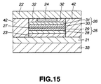
- Fig. 15 is a brief cross sectional view showing a production step of the tunneling magnetoresistive head, wherein an upper shield layer of a predetermined configuration is formed on the main surface from which the resist pattern has been removed.
-
- Description will now be directed to preferred embodiments of the present invention with reference to the attached drawings.
- It should be noted that in the drawings used in the explanation below, essential portions are sometimes enlarged and the dimensional ratio of the components may not be identical to the actual ratio.
- Firstly, explanation will be given on the magnetic tunnel junction element according to the present invention.
- As shown in Fig. 1, the magnetic tunnel junction element has a layered configuration of a first magnetic metal layer 1 and a second
magnetic metal layer 2 which are layered via atunnel barrier layer 3. Afirst electrode 4a and asecond electrode 4b are connected to the first magnetic metal layer 1 and the secondmagnetic metal layer 2, respectively. - Fig. 2 shows an enlarged perspective view of the portion in the magnetic tunnel junction element where the first magnetic metal layer 1 and the second
magnetic metal layer 2 are layered via thetunnel barrier layer 3. - In this magnetic tunnel junction element, the first magnetic metal layer 1 has a magnetization-fixed layer not changing its magnetization direction with respect to an external magnetic field. More specifically, the first magnetic metal layer 1 has a two-layered configuration having, for example, an IrMn
film 5 and aCoFe film 6 successively layered from the side of thefirst electrode 4a. - In the first magnetic metal layer 1, the IrMn
film 5 is made from an antiferromagnetic material and exchange coupling with theCoFe film 6 and fixes the magnetization of theCoFe film 6 in a predetermined direction. That is, in this magnetic tunnel junction element, theCoFe film 6 is a magnetization-fixed layer having a fixed magnetization in a predetermined direction. - On the other hand, the second
magnetic metal layer 2 has a magnetization free layer changing its magnetization direction according to an external magnetic field. More specifically, the secondmagnetic metal layer 2 has a two-layered configuration of aCoFe film 7 and a NiFefilm 8 which are successively layered from the side of thetunnel barrier layer 3. - In the second
magnetic metal layer 2, the CoFefilm 7 serves to increase the spin polarizability while the NiFefilm 8 has a low coercive force and serves as a magnetization free layer changing its magnetization direction according to an external magnetic field. The secondmagnetic metal layer 2 having such a two-layered configuration can increase the magnetoresistance ratio of the magnetic tunnel junction element. - Moreover, in this magnetic tunnel junction element, the
tunnel barrier layer 3 is formed from an insulation material such as Al2O3. - Moreover, as shown in Fig. 1 and Fig. 2, in the magnetic tunnel junction element, a non-conductive magnetic
domain control film 9 is arranged at both end portions of the secondmagnetic metal layer 2. - The magnetic
domain control film 9 is formed from a non-conductive antiferromagnetic material or a ferromagnetic material such as NiO. The NiO is a non-conductive oxide-system antiferromagnetic material and exchange coupling with the NiFe film 8 (magnetization free layer), performing a magnetic domain control of the NiFefilm 8. - Moreover, in the magnetic tunnel junction element, a portion of the NiFe film 8 (magnetization free layer) sandwiched by the magnetic
domain control films 9 serves as a magnet sensitive portion of the magnetic tunnel junction element. - This magnetic tunnel junction element is produced by a thin film formation step and the components constituting the magnetic tunnel junction element are successively layered on the
basic material 10. That is, the magnetic tunnel junction element includes thefirst electrode 4a. the first magnetic metal layer 1, thetunnel barrier layer 3, and the secondmagnetic metal layer 2 which are successively layered on thebasic material 10, and the magneticdomain control film 9 is formed at both end portions of the secondmagnetic metal layer 2, and thesecond electrode 4b is formed thereon. - More specifically, when producing the magnetic tunnel junction element, the
basic material 10 includes, for example, an insulation layer of SiO2, formed on asubstrate 11 having smoothing surface made from Si. - Moreover, in the first metal magnetic layer 1, the
IrMn film 5 is formed with a film thickness of about 10 nm and theCoFe film 6 is formed with a film thickness of about 5 nm. TheIrMn film 5 and theCoFe film 6 are successively formed by sputtering or the like. - Moreover, the
tunnel barrier layer 3 is formed by an Al2O3 film with a film thickness of about 1.3 nm. This Al2O3 film may be formed by forming an Al film on theCoFe film 6 by sputtering and oxidizing the film into Al2O3 using an oxygen plasma or the like, or by directly forming an Al2O3 film on theCoFe film 7 using the sputtering or the like. It should be noted that thetunnel barrier layer 3 is not to be limited to the Al2O3 film but may be made from any insulation material if it serves as a tunnel barrier of the so-called tunnel current, i.e., current flowing between the first magnetic metal layer 1 and the secondmagnetic metal layer 2. - Moreover, in the second
magnetic metal layer 2, theCoFe film 7 is formed with a film thickness of about 5 nm while theNiFe film 8 is formed with a film thickness of about 20 nm. TheCoFe film 7 and theNiFe film 8 are successively formed by sputtering or the like. - Moreover, the magnetic
domain control film 9 is formed by a NiO film with a film thickness of about 50 nm. The magneticdomain control film 9 is not to be limited to the NiO film but may be formed from any non-conductive antiferromagnetic material or non-conductive hard magnetic material if it can perform the magnetic domain control of theNiFe film 8. - When producing the magnetic tunnel junction element, it is possible to successively form the
IrMn film 5, the CoFe film 6 (magnetization-fixed layer), the Al2O3 film (tunnel barrier layer 3), theCoFe film 7, the NiFe film 8 (magnetization free layer), and the NiO film (magnetic domain control film 9) by sputtering or the like. These films can be successively formed with the same chamber without exposing the film materials to the atmosphere. - More specifically, firstly, the
IrMn film 5, theCoFe film 6, the Al2O3 film, theCoFe film 7, the NiFe film, and the NiO film are successively formed in the same chamber by sputtering or the like. - Next, a resist material is applied onto the NiO film to form a resist film. This resist film is patterned into a predetermined pattern using the photolithography technique so as to obtain a resist pattern. The resist pattern is formed by patterning which leaves the resist film at portions other than the magnet sensitive portion of the magnetic tunnel junction element.
- Next, this resist pattern is used as a mask when performing ion etching to remove the portion of the NiO film to serve as the magnet sensitive portion, so that the NiO film is formed at both end portions of the
NiFe film 8. - Thus, when producing the magnetic tunnel junction element, it is possible to successively form the components of the magnetic tunnel junction element in a single chamber without exposing them to the atmosphere. Accordingly, the magnetic tunnel junction element can be prepared with a high accuracy.
- In the magnetic tunnel junction element having the aforementioned configuration, when a predetermined voltage is applied between the first magnetic metal layer 1 and the second
magnetic metal layer 2, a tunnel current flows via thetunnel barrier layer 3 in the direction indicated by arrow A in Fig. 1, i.e., in the direction from the secondmagnetic metal layer 2 to the first magnetic metal layer 1. - In this magnetic tunnel junction element, the
CoFe film 6 of the first magnetic metal layer 1 serves as the magnetization-fixed layer not changing its magnetization direction while theNiFe film 8 of the secondmagnetic metal layer 2 serves as the magnetization free layer changing its magnetization direction according to an external magnetic field. For this, the CoFe film 6 (magnetization-fixed layer) is exchange coupling with theIrMn film 5 as the antiferromagnetic material and has a magnetization direction fixed in the direction indicated by arrow B in Fig. 2. On the other hand, the NiFe film 8 (magnetization free layer) is formed so as to have a uniaxial anisotropy in the direction indicated by arrow C in Fig. 2. Accordingly, when no external magnetic field is applied, theCoFe film 6 has a magnetization direction which approximately orthogonally intersects the magnetization direction of theNiFe film 8. - Moreover, the NiFe film 8 (magnetization free layer) is exchange coupling with the magnetic domain control film 9 (NiO film) formed thereon and has its magnetization direction fixed in the direction indicated by arrow C in Fig. 2. That is, the
NiFe film 8 is controlled by the magneticdomain control film 9 formed at both end portions of theNiFe film 8, so that it has a single magnetic domain in the direction identical to the direction of the uniaxial anisotropy of theNiFe film 8. Accordingly, in this magnetic tunnel junction element, it is possible to suppress the Barkhausen noise generated by a discontinuous movement of a magnetic domain of the NiFe film 8 (magnetization free layer). - Moreover, in the NiFe film 8 (magnetization free layer), since the magnetic domain control film 9 (NiO film) has electrical no-conductance, the tunnel current flows only into the magnet sensitive portion sandwiched by the magnetic
domain control films 9. - When an external magnetic field is applied to the magnetic tunnel junction element in the direction indicated by arrow D in Fig. 2, the magnetization direction of the NiFe film 8 (magnetization free layer) is changed to define a predetermined angle with the magnetization direction of the CoFe film 6 (magnetization-fixed layer). In this magnetization tunnel junction element, the resistance against the tunnel current changes depending on the relative angle between defined by the magnetization free layer and the magnetization-fixed layer. Accordingly, in this magnetic tunnel junction element, the external magnetic field change can be detected by measuring the resistance value change.
- By the way, in this magnetic tunnel junction element, as has been described above, the magnetic domain control film 9 (NiO film) having non-conductance is arranged at both end portions of the NiFe film 8 (magnetization free layer) so that the magnetic domain control of the
NiFe film 8 is performed by the magneticdomain control films 9. - Thus, in the magnetic tunnel junction element, there is no danger of electrical short circuit and the current can be made to flow only in the magnet sensitive portion of the NiFe film 8 (magnetization free layer). Accordingly, it is possible to suppress the Barkhausen noise generated by a discontinuous movement of a magnetic domain of the
NiFe film 8 and to obtain a preferable characteristic. - Next, explanation will be given on the tunneling magnetoresistive head (hereinafter, referred to as a TMR head) according to the present invention.
- As shown in Fig. 3, this TMR head includes a magnetic
tunnel junction element 20 sandwiched by alower shield layer 21 and anupper shield layer 22 via alower gap layer 23 and anupper gap layer 24. - In this TMR head, the magnetic
tunnel junction element 20 is the aforementioned magnetic tunnel junction element according to the present invention applied to a magnetic head and includes a firstmagnetic metal layer 25 and a secondmagnetic metal layer 26 which are layered via atunnel barrier layer 27. - In this magnetic
tunnel junction element 20, the firstmagnetic metal layer 25 has a magnetization-fixed layer which does not change its magnetization direction with respect to an external magnetic field. More specifically, the firstmagnetic metal layer 25, for example, has a two-layered configuration including anIrMn film 28 and aCoFe film 29 which are successively layered from the side of thelower gap layer 23. - In the first
magnetic metal layer 25, theIrMn film 28 is an antiferromagnetic material and exchange coupling with theCoFe film 29, so that the magnetization direction of theCoFe film 29 is fixed in a predetermined direction. That is, in this magnetictunnel junction element 20, theCoFe film 29 serves as a magnetization-fixed layer having a fixed magnetization in a predetermined direction. - On the other hand, the second
magnetic metal layer 26 has a magnetization free layer which changes its magnetization direction according to an external magnetic field. More specifically, the secondmagnetic metal layer 26, for example, has a two-layered configuration including aCoFe film 30 and aNiFe film 31 which are successively layered from the side of thetunnel barrier layer 27. - In the second
magnetic metal layer 26, theCoFe film 30 is used to increase the spin polarizability while theNiFe film 31 has a low coercive force and serves as a magnetization free layer changing its magnetization direction according to an external magnetic field. The secondmagnetic metal layer 26 having such a two-layered configuration can increase the magnetic resistance ratio of the magnetictunnel junction element 20. - Moreover, in the magnetic
tunnel junction element 20, thetunnel barrier layer 27 is formed, for example, from an insulation material such as Al2O3. - Moreover, the magnetic
tunnel junction element 20 includes a non-conducting magneticdomain control film 32 arranged at both end portions of the medium facing sides on the NiFe film 31 (magnetization free layer). This magneticdomain control film 32 is made from a non-conducting antiferromagnetic material or ferromagnetic material such as NiO. The NiO is a non-conducting oxide-system antiferromagnetic material exchange coupling with theNiFe film 31 and performs a magnetic domain control of theNiFe film 31. - It should be noted that in this TMR head, one end surface exposed externally is the medium facing surface to face a magnetic recording medium and the portion sandwiched by the
NiFe film 31 and the magneticdomain control film 32 in the magnetictunnel junction element 20 serves as a magnet sensitive portion of the magnetictunnel junction element 20. - Moreover, in the TMR head, the
upper shield layer 22 and thelower shield layer 21 are made from a magnetic material having electric conductivity. Moreover, theupper gap layer 24 and thelower gap layer 23 is made from a non-magnetic material having electric conductivity. - Thus, in the TMR head, the first
magnetic metal layer 25 is magnetically isolated from thelower shield layer 21, and the secondmagnetic metal layer 26 is also magnetically isolated from theupper shield layer 22. - Moreover, in the TMR head, since the
lower shield layer 21, thelower gap layer 23, theupper gap layer 24, and theupper shield layer 22 are made from a material having electric conductivity, thelower shield layer 21 and thelower gap layer 23 serve as an electrode with respect to the firstmagnetic metal layer 25 while theupper shield layer 22 and theupper gap layer 24 serve as an electrode with respect to the secondmagnetic metal layer 26. - By the way, the TMR head is produced by a thin film formation step which will be detailed later and the components constituting this TMR head are successively layered on the
substrate 33. - Moreover, this TMR head includes an insulation material filled in a space defined between the
substrate 33 and theupper shield layer 22. More specifically, in the TMR head, thelower gap layer 23, the magnetictunnel junction element 20, the magneticdomain control film 32, and theupper gap layer 24 are formed so as to be buried in the insulation material. Moreover, on the end portion of thelower shield layer 21, there is arranged aconnection terminal 34 formed from a conductive material and having a height reaching theupper shield layer 22. - It should be noted that the insulation material filled in the TMR head is omitted in the figure.
- When the TMR head having the aforementioned configuration is subjected to a signal magnetic field from a magnetic recording medium, the magnetization direction of the NiFe film 31 (magnetization free layer) changes with respect to the CoFe film 29 (magnetization-fixed layer) having a magnetic domain fixed in a predetermined direction.
- Here, a predetermined voltage is applied between the
lower shield layer 21 and theupper shield layer 22 and a tunnel current is flowing from the secondmagnetic metal layer 26 to the firstmagnetic metal layer 25 via thetunnel barrier layer 27. In the TMR head, when the magnetization direction of the NiFe film 31 (magnetization free layer) is changed to change a relative angle with respect to the magnetization direction of the CoFe film 29 (magnetization-fixed layer), the resistance value with respect to the tunnel current is changed. Thus, in the TMR head, it is possible to detect a signal magnetic field from the magnetic recording medium. - By the way, in the TMR head, the non-conducting magnetic
domain control film 32 is arranged at both end portions of the medium facing side on the NiFe film 31 (magnetization free layer) and this magneticdomain control film 32 performs the magnetic domain control of theNiFe film 31. - Thus, in this TMR head, electric current can flow only in the magnet sensitive portion of the NiFe film 8 (magnetization free layer) without causing an electric short circuit. Accordingly, it is possible to suppress the Barkhausen noise generated by a discontinuous movement of a magnetic domain of the
NiFe film 8 and stabilize the reproduction output. - Next, explanation will be given on a specific production method of the aforementioned TMR head.
- When producing the TMR head, firstly, as shown in Fig. 4, an AlTiC-system or TiO-CaO-
system substrate 33 is prepared as such that is usually used for producing a thin film type magnetic head. On one main surface of thissubstrate 33, amagnetic metal film 35 is formed from sendust or the like to serve as thelower shield layer 21 and then anon-magnetic metal film 36 is formed from Ta or the like to serve as thelower gap layer 23. Here, thenon-magnetic metal film 36 is used as the undercoat layer of the magnetictunnel junction element 20 and preferably has a highly flattened surface. - Next, as shown in Fig. 5, on the
non-magnetic metal film 36, anIrMn film 28 and aCoFe film 29 are successively formed to serve as the firstmagnetic metal layer 25. Moreover, theIrMn film 28 is subjected to an orientation processing so that it is exchange coupling with theCoFe film 29 in an approximately parallel direction with respect to a signal magnetic field applied from a magnetic recording medium. - On the
CoFe film 29, a Al2O3 film 37 is formed to serve as thetunnel barrier layer 27. This Al2O3 film 37 is formed by forming an Al film on theCoFe film 29 and then oxidizing the Al film by oxygen plasma. In this case, the Al2O3 film 37 is controlled in oxidization by adjusting, for example, the oxidization time, the gas pressure, the oxygen partial pressure, the high frequency power, and the like. Moreover, the Al2O3 film 37 may be formed by directly forming the Al2O3 film on the CoFe film by sputtering. - Next, as shown in Fig. 6, on the Al2O3 film 37, a
CoFe film 30 and aNiFe film 31 are successively formed to serve as the secondmagnetic metal layer 26. Moreover, theCoFe film 30 and theNiFe film 31 are subjected to an orientation processing so as to have a uniaxial anisotropy in a direction approximately vertical to a signal magnetic field applied from a magnetic recording medium. - On the
NiFe film 31, anNiO film 38 is formed to serve as the magneticdomain control film 32. TheNiO film 38 is subjected to an orientation processing so as to be exchange coupling with theNiFe film 31 in a direction approximately vertical to a signal magnetic field applied from a magnetic recording medium. - Next, as shown in Fig. 7, a resist material is applied onto the
NiO film 38 to form a resist film, which is patterned into a predetermined configuration using the photolithographic technique, so as to obtain a resistpattern 39. More specifically, the resistpattern 39 is formed by such a patterning that the resist film remains on a region other than the portion to become the magnet sensitive portion on theNiFe film 31. - Next, as shown in Fig. 8, using this resist
pattern 39 as a mask, theNiO film 38 if the region not having the resistpattern 39 is etched and removed by the ion milling method or the like until theNiFe film 31 formed thereunder is exposed. Thus, theNiO film 38 and the resistpattern 39 remain on the region outside the magnet sensitive portion on theNiFe film 31. - Next, as shown in Fig. 9, with the resist
pattern 39 remaining, anon-magnetic metal film 40 such as Ta is formed by sputtering so as to serve as theupper gap layer 24. - Next, as shown in Fig. 10, together with the resist
pattern 39, thenon-magnetic metal film 40 remaining on the resistpattern 39 is peeled off and removed using an organic solvent or the like. Thus, theupper gap layer 24 is formed on the region to serve as the magnet sensitive portion on theNiFe film 31. - Next, as shown in Fig. 11, a resist material is applied onto the
upper gap layer 24 and theNiO film 38 so as to form a resist film, which is patterned into a predetermined configuration using the photolithographic technique so as to obtain a resistpattern 41. More specifically, the resistpattern 41 is formed by such a patterning that the resistpattern 41 remains on the region to become the magnetictunnel junction element 20. - Next, as shown in Fig. 12, using this resist
pattern 41 as a mask, the portion not having the resistpattern 41 is etched and removed by the ion milling method or the like until themagnetic metal film 35 formed thereunder is exposed to serve as thelower shield layer 21. Thus, on thelower shield layer 21, thelower gap layer 23 having a predetermined configuration, the firstmagnetic metal layer 25, thetunnel barrier layer 27, the secondmagnetic metal layer 26, the magneticdomain control film 32, and theupper gap layer 24 are formed. That is, the magnetictunnel junction element 20 having a predetermined configuration defined by the resistpattern 41. - Next, as shown in Fig. 13, with the resist
pattern 41 remaining, aninsulation film 42 is formed by sputtering or the like so as to have almost identical height as the boundary between the resistpattern 41 and the magneticdomain control film 32 and theupper gap layer 24. - Next, as shown in Fig. 14, the
insulation film 42 remaining on the resistpattern 41 is peeled off and removed together with the resistpattern 41 using an organic solvent or the like. Thus, the magnetictunnel junction element 20 is arranged as being buried in theinsulation film 42. - Next, as shown in Fig. 15, on the main surface from which the resist
pattern 41 has been removed, theupper shield layer 22 having a predetermined configuration is formed. Theupper shield layer 22 may be formed by plating using a resist pattern having a predetermined configuration applied to the magnetic metal film to become theupper shield layer 22, or forming the magnetic metal film to become theupper shield layer 22 by sputtering and then etching it into a predetermined configuration. - Photolithography and etching are used to form the
insulation film 42 and thelower shield layer 21 into a predetermined configuration. Moreover, an opening is formed in theinsulation film 42 on the end portion of thelower shield layer 21, so as to expose thelower shield layer 21. This opening is filled with a conducting material and aconnection terminal 34 is formed on thelower shield layer 21. Thus, thelower shield layer 21 can be electrically connected together with theupper shield layer 22. - As has been described above, the tunneling magnetoresistive head as shown in Fig. 3 is prepared.
- According to this method, it is possible to successively perform the film formation process of the components constituting the TMR head, the etching process, or the Al film oxidization process in a single chamber without exposing the components to the atmosphere. Accordingly, it is possible to produce the TMR head with a high accuracy.
- As has been described above, the magnetic tunnel junction element according to the present invention having the non-conducting magnetic domain control film formed at both end portions of the medium facing side of the second magnetic layer can suppress generation of the Barkhausen noise without causing an electric short circuit and obtain a preferable characteristic.
- Moreover, according to the magnetic tunnel junction element production method according to the present invention, the components of the magnetic tunnel junction element can be successively formed in a single apparatus without exposing them to the atmosphere, thereby enabling to prepare the magnetic tunnel junction element with a high accuracy.
- Moreover, in the tunneling magnetoresistive head according to the present invention, the non-conducting magnetic domain control film is formed at both end portions of the medium facing side of the second magnetic layer of the magnetic tunnel junction element and accordingly, no electric short circuit is generated. Thus, it is possible to suppress generation of the Barkhausen noise and stabilize the reproduction output.
- Moreover, according to the tunneling magnetoresistive head production method according to the present invention, it is possible to successively form the components of the tunneling magnetoresistive head in a single apparatus without exposing the components to the atmosphere. Thus, it is possible to prepare the tunneling magnetoresistive head with a high accuracy.
Claims (8)
- A magnetic tunnel junction element comprising:a first magnetic layer having magnetization fixed in a predetermined direction,an insulation layer formed on said first magnetic layer, anda second magnetic layer formed on said insulation layer and changing its magnetization direction according to an external magnetic field,
wherein said second magnetic layer is provided with non-conducting magnetic domain control films formed at both end portions on said second magnetic layer. - The magnetic tunnel junction element as claimed in Claim 1, wherein said magnetic domain control film is made from an oxide-system antiferromagnetic material.
- A magnetic tunnel junction element production method comprising steps of:forming a first magnetic layer having its magnetization direction fixed in a predetermined direction,forming an insulation layer on said first magnetic layer,forming a second magnetic layer on said insulation layer so as to change its magnetization direction according to an external magnetic field,forming a non-conducting magnetic domain control film on said second magnetic layer,forming a resist pattern having a predetermined configuration on said magnetic domain control film, andremoving said magnetic domain control film by etching using said resist pattern excluding the both end portions on said second magnetic layer.
- The magnetic tunnel junction element production method as claimed in Claim 3, wherein said magnetic domain control film is formed using an oxide-system antiferromagnetic material.
- A tunneling magnetoresistive head comprising a first magnetic layer having magnetization fixed in a predetermined direction, an insulation layer formed on said first magnetic layer, a second magnetic layer formed on said insulation layer and changing its magnetization direction according to an external magnetic field,
wherein said second magnetic layer is provided with non-conducting magnetic domain control films on both end portions thereof. - The tunneling magnetoresistive head as claimed in Claim 5, wherein said magnetic domain control film is made from an oxide-system antiferromagnetic material.
- A tunneling magnetoresistive head production method in which a magnetic tunnel junction element is produced by steps of:forming a first magnetic layer having its magnetization direction fixed in a predetermined direction,forming an insulation layer on said first magnetic layer,forming a second magnetic layer on said insulation layer so as to change its magnetization direction according to an external magnetic field,forming a non-conducting magnetic domain control film on said second magnetic layer,forming a resist pattern having a predetermined configuration on said magnetic domain control film, andremoving said magnetic domain control film by etching using said resist pattern excluding the both end portions on said second magnetic layer.
- The tunneling magnetoresistive head production method as claimed in Claim 7 wherein said magnetic domain control film is formed using an oxide-system antiferromagnetic material.
Applications Claiming Priority (2)
| Application Number | Priority Date | Filing Date | Title |
|---|---|---|---|
| JP31429199A JP2001134913A (en) | 1999-11-04 | 1999-11-04 | Magnetic tunnel junction element, its manufacturing method, magnetic tunnel effect type magnetic head and its manufacturing method |
| JP31429199 | 1999-11-04 |
Publications (1)
| Publication Number | Publication Date |
|---|---|
| EP1098203A2 true EP1098203A2 (en) | 2001-05-09 |
Family
ID=18051606
Family Applications (1)
| Application Number | Title | Priority Date | Filing Date |
|---|---|---|---|
| EP00123750A Withdrawn EP1098203A2 (en) | 1999-11-04 | 2000-10-31 | Magnetic tunnel junction element, tunneling magnetoresistive head, and production methods |
Country Status (2)
| Country | Link |
|---|---|
| EP (1) | EP1098203A2 (en) |
| JP (1) | JP2001134913A (en) |
-
1999
- 1999-11-04 JP JP31429199A patent/JP2001134913A/en active Pending
-
2000
- 2000-10-31 EP EP00123750A patent/EP1098203A2/en not_active Withdrawn
Also Published As
| Publication number | Publication date |
|---|---|
| JP2001134913A (en) | 2001-05-18 |
Similar Documents
| Publication | Publication Date | Title |
|---|---|---|
| US6198378B1 (en) | Magnetoresisitive sensor and manufacturing method therefor | |
| US5946167A (en) | Magnetoresistive sensor having lead and/or bias layer structure contributing to a narrow gap | |
| KR19990083593A (en) | Spin tunnel magneto-resistance effect type magnetic sensor and production method thereof | |
| US6519123B1 (en) | Method to manufacture magnetic tunneling elements using inductively coupled plasma | |
| JP2001084535A (en) | Manufacture of thin film magnetic head and manufacture of magnetresistance effect device | |
| JP3680655B2 (en) | Magnetoresistive element and manufacturing method thereof | |
| US6621666B2 (en) | Magnetoresistive-effect element having electrode layers oppositely disposed on main surfaces of a magnetoresistive-effect thin film having hard magnetic bias layers with a particular resistivity | |
| JP2002163809A (en) | Method for manufacturing magneto-resistive element and magneto-resistive magnetic head | |
| JP2004152334A (en) | Magnetic sensor, its manufacturing method and magnetic recording and reproducing device employing the sensor | |
| EP0762389B1 (en) | Magnetoresistive head, manufacturing method of the head and magnetic recording/reproducing drive | |
| JP2003059008A (en) | Magneto-resistance head and manufacturing method thereof | |
| US7201947B2 (en) | CPP and MTJ reader design with continuous exchange-coupled free layer | |
| US6718623B2 (en) | Magnetoresistive device and method of manufacturing same, and thin-film magnetic head and method of manufacturing same | |
| US20050068687A1 (en) | Magnetoresistance effect element, method of manufacturing same and magnetic head utilizing same | |
| US6842314B2 (en) | Magnetoresistive device and method of manufacturing same, and thin-film magnetic head and method of manufacturing same | |
| EP1098203A2 (en) | Magnetic tunnel junction element, tunneling magnetoresistive head, and production methods | |
| JPH10163544A (en) | Magnetoresistive effect element and manufacture thereof | |
| US6433969B1 (en) | Compound magnetoresistive head and method for manufacturing same | |
| JP2002015407A (en) | Thin film magnetic head and method of manufacture | |
| JP2000187813A (en) | Joint structure, magneto-resistance effect element, and manufacture thereof | |
| JP2000113419A (en) | Magnetic head provided with magnetoresistive element | |
| JP2006004492A (en) | Magnetoresistive head | |
| JPWO2003083838A1 (en) | Magnetoresistive sensor and manufacturing method thereof | |
| JP2001084522A (en) | Sensor for polishing, bar block for thin film element equipped with the sensor, and wafer substrate for thin film element equipped with the sensor | |
| KR100668405B1 (en) | Magneto-resistive head |
Legal Events
| Date | Code | Title | Description |
|---|---|---|---|
| PUAI | Public reference made under article 153(3) epc to a published international application that has entered the european phase |
Free format text: ORIGINAL CODE: 0009012 |
|
| AK | Designated contracting states |
Kind code of ref document: A2 Designated state(s): AT BE CH CY DE DK ES FI FR GB GR IE IT LI LU MC NL PT SE |
|
| AX | Request for extension of the european patent |
Free format text: AL;LT;LV;MK;RO;SI |
|
| STAA | Information on the status of an ep patent application or granted ep patent |
Free format text: STATUS: THE APPLICATION HAS BEEN WITHDRAWN |
|
| 18W | Application withdrawn |
Effective date: 20021211 |