EP1096679A2 - Pulse width modulation for correcting non-uniformity of acoustic inkjet printhead - Google Patents
Pulse width modulation for correcting non-uniformity of acoustic inkjet printhead Download PDFInfo
- Publication number
- EP1096679A2 EP1096679A2 EP00309155A EP00309155A EP1096679A2 EP 1096679 A2 EP1096679 A2 EP 1096679A2 EP 00309155 A EP00309155 A EP 00309155A EP 00309155 A EP00309155 A EP 00309155A EP 1096679 A2 EP1096679 A2 EP 1096679A2
- Authority
- EP
- European Patent Office
- Prior art keywords
- pulse
- edge
- width modulation
- delay
- delay data
- Prior art date
- Legal status (The legal status is an assumption and is not a legal conclusion. Google has not performed a legal analysis and makes no representation as to the accuracy of the status listed.)
- Granted
Links
Images




Classifications
-
- B—PERFORMING OPERATIONS; TRANSPORTING
- B41—PRINTING; LINING MACHINES; TYPEWRITERS; STAMPS
- B41J—TYPEWRITERS; SELECTIVE PRINTING MECHANISMS, i.e. MECHANISMS PRINTING OTHERWISE THAN FROM A FORME; CORRECTION OF TYPOGRAPHICAL ERRORS
- B41J2/00—Typewriters or selective printing mechanisms characterised by the printing or marking process for which they are designed
- B41J2/005—Typewriters or selective printing mechanisms characterised by the printing or marking process for which they are designed characterised by bringing liquid or particles selectively into contact with a printing material
- B41J2/01—Ink jet
- B41J2/015—Ink jet characterised by the jet generation process
- B41J2/04—Ink jet characterised by the jet generation process generating single droplets or particles on demand
- B41J2/045—Ink jet characterised by the jet generation process generating single droplets or particles on demand by pressure, e.g. electromechanical transducers
- B41J2/04501—Control methods or devices therefor, e.g. driver circuits, control circuits
- B41J2/04541—Specific driving circuit
-
- B—PERFORMING OPERATIONS; TRANSPORTING
- B41—PRINTING; LINING MACHINES; TYPEWRITERS; STAMPS
- B41J—TYPEWRITERS; SELECTIVE PRINTING MECHANISMS, i.e. MECHANISMS PRINTING OTHERWISE THAN FROM A FORME; CORRECTION OF TYPOGRAPHICAL ERRORS
- B41J2/00—Typewriters or selective printing mechanisms characterised by the printing or marking process for which they are designed
- B41J2/005—Typewriters or selective printing mechanisms characterised by the printing or marking process for which they are designed characterised by bringing liquid or particles selectively into contact with a printing material
- B41J2/01—Ink jet
- B41J2/015—Ink jet characterised by the jet generation process
- B41J2/04—Ink jet characterised by the jet generation process generating single droplets or particles on demand
- B41J2/045—Ink jet characterised by the jet generation process generating single droplets or particles on demand by pressure, e.g. electromechanical transducers
- B41J2/04501—Control methods or devices therefor, e.g. driver circuits, control circuits
- B41J2/04573—Timing; Delays
-
- B—PERFORMING OPERATIONS; TRANSPORTING
- B41—PRINTING; LINING MACHINES; TYPEWRITERS; STAMPS
- B41J—TYPEWRITERS; SELECTIVE PRINTING MECHANISMS, i.e. MECHANISMS PRINTING OTHERWISE THAN FROM A FORME; CORRECTION OF TYPOGRAPHICAL ERRORS
- B41J2/00—Typewriters or selective printing mechanisms characterised by the printing or marking process for which they are designed
- B41J2/005—Typewriters or selective printing mechanisms characterised by the printing or marking process for which they are designed characterised by bringing liquid or particles selectively into contact with a printing material
- B41J2/01—Ink jet
- B41J2/015—Ink jet characterised by the jet generation process
- B41J2/04—Ink jet characterised by the jet generation process generating single droplets or particles on demand
- B41J2/045—Ink jet characterised by the jet generation process generating single droplets or particles on demand by pressure, e.g. electromechanical transducers
- B41J2/04501—Control methods or devices therefor, e.g. driver circuits, control circuits
- B41J2/04575—Control methods or devices therefor, e.g. driver circuits, control circuits controlling heads of acoustic type
-
- B—PERFORMING OPERATIONS; TRANSPORTING
- B41—PRINTING; LINING MACHINES; TYPEWRITERS; STAMPS
- B41J—TYPEWRITERS; SELECTIVE PRINTING MECHANISMS, i.e. MECHANISMS PRINTING OTHERWISE THAN FROM A FORME; CORRECTION OF TYPOGRAPHICAL ERRORS
- B41J2/00—Typewriters or selective printing mechanisms characterised by the printing or marking process for which they are designed
- B41J2/005—Typewriters or selective printing mechanisms characterised by the printing or marking process for which they are designed characterised by bringing liquid or particles selectively into contact with a printing material
- B41J2/01—Ink jet
- B41J2/015—Ink jet characterised by the jet generation process
- B41J2/04—Ink jet characterised by the jet generation process generating single droplets or particles on demand
- B41J2/045—Ink jet characterised by the jet generation process generating single droplets or particles on demand by pressure, e.g. electromechanical transducers
- B41J2/04501—Control methods or devices therefor, e.g. driver circuits, control circuits
- B41J2/04588—Control methods or devices therefor, e.g. driver circuits, control circuits using a specific waveform
-
- B—PERFORMING OPERATIONS; TRANSPORTING
- B41—PRINTING; LINING MACHINES; TYPEWRITERS; STAMPS
- B41J—TYPEWRITERS; SELECTIVE PRINTING MECHANISMS, i.e. MECHANISMS PRINTING OTHERWISE THAN FROM A FORME; CORRECTION OF TYPOGRAPHICAL ERRORS
- B41J2/00—Typewriters or selective printing mechanisms characterised by the printing or marking process for which they are designed
- B41J2/005—Typewriters or selective printing mechanisms characterised by the printing or marking process for which they are designed characterised by bringing liquid or particles selectively into contact with a printing material
- B41J2/01—Ink jet
- B41J2/015—Ink jet characterised by the jet generation process
- B41J2/04—Ink jet characterised by the jet generation process generating single droplets or particles on demand
- B41J2/045—Ink jet characterised by the jet generation process generating single droplets or particles on demand by pressure, e.g. electromechanical transducers
- B41J2/04501—Control methods or devices therefor, e.g. driver circuits, control circuits
- B41J2/04591—Width of the driving signal being adjusted
-
- B—PERFORMING OPERATIONS; TRANSPORTING
- B41—PRINTING; LINING MACHINES; TYPEWRITERS; STAMPS
- B41J—TYPEWRITERS; SELECTIVE PRINTING MECHANISMS, i.e. MECHANISMS PRINTING OTHERWISE THAN FROM A FORME; CORRECTION OF TYPOGRAPHICAL ERRORS
- B41J2/00—Typewriters or selective printing mechanisms characterised by the printing or marking process for which they are designed
- B41J2/005—Typewriters or selective printing mechanisms characterised by the printing or marking process for which they are designed characterised by bringing liquid or particles selectively into contact with a printing material
- B41J2/01—Ink jet
- B41J2/135—Nozzles
- B41J2/14—Structure thereof only for on-demand ink jet heads
- B41J2/14008—Structure of acoustic ink jet print heads
-
- H—ELECTRICITY
- H03—ELECTRONIC CIRCUITRY
- H03K—PULSE TECHNIQUE
- H03K5/00—Manipulating of pulses not covered by one of the other main groups of this subclass
- H03K5/01—Shaping pulses
- H03K5/04—Shaping pulses by increasing duration; by decreasing duration
- H03K5/05—Shaping pulses by increasing duration; by decreasing duration by the use of clock signals or other time reference signals
-
- H—ELECTRICITY
- H03—ELECTRONIC CIRCUITRY
- H03K—PULSE TECHNIQUE
- H03K7/00—Modulating pulses with a continuously-variable modulating signal
- H03K7/08—Duration or width modulation ; Duty cycle modulation
-
- B—PERFORMING OPERATIONS; TRANSPORTING
- B41—PRINTING; LINING MACHINES; TYPEWRITERS; STAMPS
- B41J—TYPEWRITERS; SELECTIVE PRINTING MECHANISMS, i.e. MECHANISMS PRINTING OTHERWISE THAN FROM A FORME; CORRECTION OF TYPOGRAPHICAL ERRORS
- B41J2/00—Typewriters or selective printing mechanisms characterised by the printing or marking process for which they are designed
- B41J2/005—Typewriters or selective printing mechanisms characterised by the printing or marking process for which they are designed characterised by bringing liquid or particles selectively into contact with a printing material
- B41J2/01—Ink jet
- B41J2/135—Nozzles
- B41J2/14—Structure thereof only for on-demand ink jet heads
- B41J2002/14322—Print head without nozzle
Definitions
- This invention relates to correcting non-uniformity of size or ejection velocity of each individual droplet of acoustic inkjet printheads and more particularly to an acoustic inkjet printhead where the RF signal delivered to each transducer is individually controlled to provide a desired droplet size or ejection velocity.
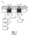
- Printhead 10 has a liquid level control structure 12 which captures an ink layer 16 over a glass substrate 14.
- Liquid level control structure 12 has a plurality of apertures 18 each of which is dedicated to a single acoustic ejector.
- Under the glass substrate there is a plurality of piezo-electric transducers 20.
- piezo-electric transducer is referred to as "transducer.”
- Each transducer 20 is dedicated to one aperture 18 and is located directly across its respective aperture 18. Once each transducer 20 is activated, it will oscillate and generate acoustic waves 22 which travel within the glass substrate 14 toward the ink 16.
- Fresnel lenses 24 Over the glass substrate 14, there is a plurality of Fresnel lenses 24, each of which corresponds to one of the transducers 20 and is located across from its respective transducer 20.
- the Fresnel lenses 24 receive the acoustic waves 22 from the transducers 20 and focus the acoustic waves onto the liquid surface in their respective apertures 18.
- the focused waves 22 cause the ink to be ejected from the apertures as droplets 26.
- Oscillator 30 generates a RF signal and sends it to a RF Amplifier 32 to be amplified.
- the amplified RF signal is sent to several RF power switches 34.
- Each output of each power switch 34 is distributed between the plurality of transducers 20 where each transducer 20 is grounded through its individual switch Z.
- Switches Z control the time and duration of the RF signal applied to each transducer 20. Once each switch Z is closed, the RF signal flows into the respective transducer 20 and once the switch is opened, the flow of the RF signal into the transducer 20 will be significantly reduced. The time each switch Z is closed determines the duration of the RF signal applied to the transducers. All switches Z receive the same control signal C from a switch driver circuit 36.
- Non-uniformity of droplet size 18 creates different size pixels which can be observed as variation of the thickness of a line.
- non-uniformity of ejection velocity causes pixels not to align on a straight line. Since the paper is moving, in order to have a straight line, all the droplets have to be ejected at the same time to strike the paper at the same time. If a droplet is ejected before or after the intended time, the pixel on the paper will be above or below the intended line respectively.
- Non uniformity of the droplet size and velocity are two problems of the prior art acoustic ink jet printheads.
- a method of correcting non-uniformity of droplet size or ejection velocity by pulse width modulation comprises the steps of receiving a pulse with a first pulse edge and a second pulse edge and delaying the first pulse edge of said pulse according to a plurality of predetermined delay data to create a plurality of delayed first pulse edges. Subsequently, sending out each delayed first pulse edge with the received second pulse edge of the pulse as the first pulse edge and second pulse edge of a control pulse to create a plurality of control pulses with different pulse widths.
- an apparatus for correcting non-uniformity of droplet size or ejection velocity by pulse width modulation comprises a delaying means.
- the delaying means receives a pulse and creates a plurality of control pulses.
- the received pulse has a first pulse edge and a second pulse edge.
- a lookup table stores an individual delay data for each of the plurality of control pulses.
- the delaying means is in communication with the lookup table to receive the plurality of delay data.
- the delaying means is responsive to the delay data from the lookup table to delay only the first pulse edge of the pulse according to each of the delay data to create a plurality of delayed first pulse edges.
- the delaying means sends out each of the plurality of delayed first pulse edges in combination with the received second pulse edge of the pulse as the first pulse and second pulse edges of a control pulse to create a plurality of control pulses with different pulse widths.
- Printhead 42 comprises a liquid level control structure 44, a sheet of glass substrate 46, ink 48 over the glass substrate 46, a plurality of Fresnel lenses 50 over the glass substrate 46 within the ink 48, and a plurality of transducers 52 under the glass substrate 46.
- the acoustic inkjet driver circuit 40 supplies a RF signal to all transducers 52 where each transducer 52 is grounded through an individual switch Z 1 .
- a RF power source 54 generates and sends a RF signal to the plurality of transducers 52 through an amplifier 56 and a plurality of power switches 58.
- a control block 60 within the acoustic inkjet driver circuit 40, has an individual connection (CS 1 , CS 2 , ...) to each switch Z 1 to individually control (activate or inactivate) switches Z 1 . Once activated, each switch Z 1 causes the RF signal to flow into its respective transducer 52 and once inactivated, the flow will be significantly reduced.
- Control block 60 is capable of modifying the RF signal applied to each transducer 52 to generate a droplet with a desired size or velocity.
- the duration of the RF signal applied to each transducer 52 is modified according to the correction data for each transducer to produce a desired spot size or velocity. This is accomplished by controlling the duration of the time that each switch Z 1 is active through the control block 60.
- each switch Z 1 The activation time (rising edge of control signal) of each switch Z 1 is customized to the requirement of its respective transducer 52. However, all switches Z 1 will be inactivated (falling edge of control signal) by the system at the same time. In other words, switches Z 1 will be activated at different times, but inactivated at the same time. This causes each transducer 52 to receive the RF signal at a different time for a different duration.
- FIG. 5 there is shown a block diagram of the control block 60 of Figure 2 which receives a serial data from a look up table 66.
- the look up table 66 contains the correction data for the width of the control signal of each switch Z 1 .
- the correction data is a number (delay value) V 1 -V 3 2 represented by six bits which is sent out serially.
- Control block 60 receives the serial data from the look up table 66 and places each six consecutive bits, which represent one correction data, in an addressable location 68 of a RAM 70.
- RAM 70 has 32 addressable locations 68 to hold correction data for 32 transducers 52 of one column of a two dimensional array of transducers 52.
- the number of addressable locations of the RAM 70 can be modified to accommodate any number of transducers. Therefore, the concept of this invention should not be limited to the number of transducers in a column or a row. The concept can be applied to any number of transducers on a printhead.
- RAM 70 has six outputs 72 for each addressable location 68. When one addressable location 68 of RAM 70 is activated, the six bit data stored in that location is sent out to the six outputs 72 to provide as a parallel output data. The parallel output data 72 of each location 68 is sent to the pulse width modulator (PWM) block 74.
- PWM pulse width modulator
- the PWM 74 receives a system activation pulse as input pulse IP from the system (printer).
- the rising edge of the input pulse IP is used to activate all switches.
- the rising edge of the input pulse IP is used to activate the PWM 74.
- the PWM block 74 takes the parallel output data 72 from all the locations 68 of the RAM 70.
- Each six bits 72 from each addressable location 68 is delivered to one of the blocks DL 1 -DL 32 . For the purpose of simplicity, only the connection of the outputs 72 of one of the addressable locations 68 to its respective block DL2 is shown.
- Each block DL 1 -DL 32 receives the input pulse IP, reads the number represented by the six bits 72, and delays the rising edge of the input pulse IP according to the received number. However, when blocks DL 1 -DL 32 receive the falling edge of the input pulse IP, they will be rested and their outputs will become zero. As a result, blocks DL 1 -DL 32 delay the rising edge of the input pulse IP, but send out the falling edge of the input pulse IP without any delay. In this specification, delaying the rising edge without delaying the falling edge or visa versa is defined as pulse width modulation.
- Each delayed input pulse IP d1 -IP d32 is sent to an AND gate 80.
- Each AND gate 80 receives an individual selection signal M 1 -M 32 which selects the activation of its respective switch Z 1 . Once any one of the selection signals M 1 -M 32 is high (1), then the respective AND gate 80 sends out the delayed pulse IP d1 -IP d32 as a control pulse CS 1 -CS 32 to their respective switches Z 1 .
- the block diagram 60 modifies the time and duration of the RF signal applied to each transducer to provide a desired spot size for each droplet. Changing the duration of the RF signal also changes the energy applied to each transducer which causes the velocity of the ejection to change. If the printed lines have droplet size errors, a correction data can be created based on the droplet size errors. However, if the printed line has jagged pixels, then a correction data based on the ejection velocity error can be created. The disclosed embodiment of this invention can correct either the droplet size or the ejection velocity depending on if it receives correction data for droplet size or correction data for ejection velocity respectively. Therefore, the look up table 66 of Figure 5 can either hold correction data for droplet size or correction data for ejection velocity.
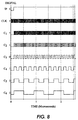
- a clock divider CD divides the system clock CLK and generates 6 clocks C 1 , C 2 , C 3 , C 4 , C 5 , and C 6 with periods of T, 2T, 4T, 8T, 16T, and 32T and sends them to the delay logic blocks DL 1 ⁇ DL 32 of different lines.
- flip flop F 0 is placed in the path of system clock CLK to the clock divider CD.
- the D input of flip flop F 0 is connected to VDD to continuously keep the D input of flip flop F 0 at high (1).
- the positive output (Q) of F 0 is connected to the clock divider CD.
- the input pulse which needs to be delayed, is connected to the Reset line of the F 0 through an inverter I 0 .
- the clock input of flip flop F 0 receives the system clock CLK.
- flip flop F 0 keeps the system clock CLK until it receives the rising edge of IP which inactivates the reset of flip flop F 0 . Then, F 0 sends out the system clock as a synchronized clock CLK S to the CD block. Since CLK S is synchronized with the input pulse IP, the input pulse IP will receive full delays.
- FIG. 7 there is shown a detail block diagram of the clock divider CD of Figure 6.
- the system reset input pulse IP is sent to the reset pin of flip flops F 1 , F 2 , F 3 , F 4 , and F 5 through inverter I 11 .
- the synchronized system clock CLK S and the input pulse IP are sent to an AND gate A 1 to generate a resetable clock C 1 with the same period as the synchronized system clock CLK S .
- To divide clock C 1 five flip flops F 1 , F 2 , F 3 , F 4 , and F 5 are used.
- C 1 is sent to F 1 as a clock.
- each flip flop F 1 , F 2 , F 3 , F 4 , and F 5 is connected to its input. This configuration causes each flip flop F 1 , F 2 , F 3 , F 4 , and F 5 to divide its clock by 2.
- the positive output (Q) of each flip flop F 1 , F 2 , F 3 , F 4 , and F 5 is connected to the clock of the following flip flop.
- the positive output of flip flops F 1 , F 2 , F 3 , F 4 , and F 5 are sent out as clocks C 2 , C 3 , C 4 , C 5 , and C 6 respectively.
- each flip flop F 1 , F 2 , F 3 , F 4 , and F 5 divides its clock by 2 and sends it out on its positive output
- C 2 has a period twice as its input clock. Since the period of clock C 1 is equal to the period T of the synchronized system clock CLKs, the period of clock C 2 is 2T. In the same manner, the periods of clocks C 3 , C 4 , C 5 , and C 6 are 4T, 8T, 16T, and 32T as shown in Figure 8.
- clocks C 1 , C 2 , C 3 , C 4 , C 5 , and C 6 are sent to all delay bocks DL 1 ⁇ DL3 2 where each delay block selects a combination of the clocks C 1 , C 2 , C 3 , C 4 , C 5 , and C 6 to create a required delay.
- Each delay block DL 1 -DL 32 receives the input pulse IP and a six bit delay value V 1 -V 32 via the outputs 72 of Figure 5.
- each delay block DL 1 -DL 32 delays the input pulse IP according to its respective delay value V 1 -V 32 and sends it out on its output OUT 1 -OUT 32 respectively.
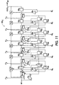
- delay block DL 1 there is shown a logic diagram one of the delay block DL 1 .
- the delay blocks DL 2 -DL 32 are identical to DL 1 .
- delay block DL 1 there are six D flip flops FF 1 , FF 2 , FF 3 , FF 4 , FF 5 , FF 6 .
- the clock inputs of the flip flops FF 1 , FF 2 , FF 3 , FF 4 , FF 5 , FF 6 are connected to the clocks C 6 , C 5 , C 4 , C 3 , C 2 , and C 1 respectively.
- each flip flop FF 1 , FF 2 , FF 3 , FF 4 , and FF 5 is connected to the input of the following flip flop through switches SS 1 , SS 2 , SS 3 , SS 4 , and SS 5 respectively.
- the positive output of flip flop FF 6 is connected to the output OUT 1 through switch SS 6 .
- the output OUT1 provides the IP d1 of Figure 5.
- the input of each flip flop FF 1 , FF 2 , FF 3 , FF 4 , FF 5 , FF 6 is connected to the input of the following flip flop through switches S 1 , S 2 , S 3 , S 4 , S 5 , and S 6 respectively.
- Each delay block DL 1 -DL 32 of Figure 6 receives a separate delay value through V 1 -V 32 respectively.
- Each V 1 -V 32 has six bits B 1 , B 2 , B 3 , B 4 , B 5 , and B 6 which deliver a number between 0 to 63.
- B 1 , B 2 , B 3 , B 4 , B 5 , and B 6 are directly connected to the control pins of switches SS 1 , SS 2 , SS 3 , SS 4 , SS 5 , and SS 6 respectively and connected to the control pins of switches S 1 , S 2 , S 3 , S 4 , S 5 , and S 6 through inverters I 1 , I 2 , I 3 , I 4 , I 5 , and I 6 respectively.
- switch S 3 closes and connects the input of FF 3 to the input of FF 4 .
- switch S 3 closes and connects the input of FF 3 to the input of FF 4 .
- one of the bits B 6 , B 5 , B 4 , B 3 , B2 , and B 1 is high (1), the output of the previous flip flop is delivered to the input of the following flip flop, but if it is low (0), the previous flip flop is by passed and its input is delivered to the input of the next flip flop.
- bits B 5 , B 4 , and B 3 are zero, switches S 2 , S 3 , and S4 close, by pass flip flops FF 2 , FF 3 , and FF 4 , and deliver the output of flip flop FF 1 to the input of FF 5 .
- the outputs of the flip flops FF 1 , FF 2 , FF 3 , FF 4 , FF 5 , and FF 6 can be at don't care (unknown) state.
- flip flops FF 1 , FF 2 , FF 3 , FF 4 , FF 5 , and FF 6 have to receive a reset.
- Each flip flop FF 2 , FF 3 , FF 4 , FF 5 , and FF 6 receives a Reset signal from one of two switches (S 1A and S 1B ), (S 2A and S 2B ), (S 3A and S 3B ), (S 4A and S 4B ), and (S 5A and S 5B ) respectively.
- the control pins of switches S 1B , S 2B , S 3B , S 4B , and S 5B are connected to B 6 , B 5 , B 4 , B 3 , and B 2 respectively.
- switches S 1A , S 2A , S 3A , S 4A , and S 5A are connected to B 6 , B 5 , B 4 , B 3 , and B 2 through inverters I 1 , I 2 , I 3 , I 4 , and I 5 respectively.
- the negative output (QB) of flip flops FF 1 , FF 2 , FF 3 , FF 4 , and FF 5 are connected to the reset pin of flip flops FF 2 , FF 3 , FF 4 , FF 5 , and FF 6 through switches S 1B , S 2B , S 3B , S 4B , and S 5B .
- flip flops FF 1 , FF 2 , FF 3 , FF 4 , and FF 5 are connected to the reset pin of flip flops FF 2 , FF 3 , FF 4 , FF 5 , and FF 6 through inverters and switches (II 1 and S 1A ), (II 2 and S 2A ), (II 3 and S 3A ), (II 4 and S 4A ), and (II 5 and S 5A ) respectively.
- Flip flop FF 1 is reset by the input pulse IP through inverter II 1 .
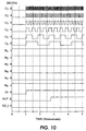
- each output will delay the rising edge of the same input pulse IP with a different delay value. Therefore, Output lines OUT 1 , OUT 2 and OUT 32 delay the rising edge of IP and send it out at t 11 , t 13 , and t 12 respectively.
- the falling edge of the input pulse IP at t 2 enters PWM block 74, all the outputs OUT 1 , OUT 2 and OUT 32 will become 0. It should be noted that each output OUT 1 -OUT 32 can have a different delay and therefore each output can have less or more delay than what is shown.
- the PWM block 74 provides pulse width modulation since each output OUT 1 -OUT 32 sends out a signal with a rising edge that has a different timing, but a falling edge concurrent with the falling edge of the signals of the other outputs OUT 1 - OUT 32 .
- the width of each output pulse is determined by its respective delay value V 1 - V 32 .
- the logic diagram of Figure 6 is designed to create 0 - 64T delays for each signal of 32 lines. However, the concept of this invention can be applied to different number of delays on different number of lines.
- FIG. 13 there is shown an alternative pulse width modulation of this invention.
- the input pulse IP is inverted through inverter I IN before applying to block DL 1 and the output OUT 1 of DL 1 is connected to inverter I OUT .
- the rising edge of the input pulse IP at t 1 will reset the DL 1 block and the falling edge of the input pulse t 2 will be delayed. Therefore, I OUT sends out a signal with a rising edge at t 2 and a falling edge at t 21 (the delayed falling edge of the input pulse IP). If this inversion is applied to all blocks DL 1 -DL 32 of Figure 6, they will provide pulse width modulation by concurrently sending out the rising edge of the input pulse and delaying the falling edge of the input pulse IP according to their respective delay values V 1 -V 32 .
Landscapes
- Physics & Mathematics (AREA)
- Nonlinear Science (AREA)
- Particle Formation And Scattering Control In Inkjet Printers (AREA)
- Pulse Circuits (AREA)
Abstract
Description
Claims (10)
- A method of pulse width modulation comprising the steps of:receiving a plurality of pulses each with a first pulse edge and a second pulse edge;delaying the first pulse edge of each one of said plurality of pulses according to a delay data predetermined for each pulse; andsending out the delayed first pulse edge of each one of said plurality of pulses and the second pulse edge of the respective received pulse as the first and second pulse edges of a modulated pulse.
- The method of pulse width modulation recited in claim 1, wherein the first pulse edge is a rising edge and the second pulse edge is a falling edge.
- The method of pulse width modulation recited in claim 1, wherein the first pulse edge is a falling edge and the second pulse edge a rising edge.
- A method of pulse width modulation according to claim 1, 2 or 3, for correcting non-uniformity of droplet size or ejection velocity of an acoustic inkjet printhead by creating an individual control signal for each transducer.
- The method recited in claim 4, wherein the delay data is data for correcting droplet size.
- The method recited in claim 4, wherein the delay data is data for correcting droplet ejection velocity.
- An apparatus for pulse width modulation comprising:a delaying means (DL1-DL32);said delaying means receiving a pulse (IP) and creating a plurality of modulated pulses;said pulse (IP) having a first pulse edge (t1) and a second pulse edge (t2);a lookup table (66) for storing an individual delay data for each of said plurality of modulated pulses;said delaying means (DL1-DL32) being in communication with said lookup table (66) for receiving said delay data;said delaying means (DL1-DL32) being responsive to said delay data from said lookup table (66) to delay only said first pulse edge of said pulse according to each of said delay data to create a plurality of delayed first pulse edges; andsaid delaying means (DL1-DL32) sending out each of said plurality of delayed first pulse edges (t1) in combination with said received second pulse edge (t2) of said pulse as the first pulse edge and second pulse edge of a modulated pulse to create a plurality of modulated pulses with different pulse widths.
- The apparatus for pulse width modulation as recited in claim 9, wherein said delaying means further comprising:a plurality of storage means being in communication with said lookup table;each of said plurality of storage means receiving and storing a delay data for one of said plurality of modulated pulses;a plurality of delaying blocks each being in communication with one of said plurality of storage means for receiving a respective delay data; andeach of said plurality of delaying blocks receiving said pulse and delaying the first pulse edge of said pulse according to a respective delay data.
- The method of pulse width modulation recited in claim 7 or 8, wherein the first pulse edge is a rising edge and the second pulse edge is a falling edge.
- The method of pulse width modulation recited in claim 7 or 8, wherein the first pulse edge is a falling edge and the second pulse edge a rising edge.
Applications Claiming Priority (2)
| Application Number | Priority Date | Filing Date | Title |
|---|---|---|---|
| US428823 | 1989-10-30 | ||
| US09/428,823 US6299272B1 (en) | 1999-10-28 | 1999-10-28 | Pulse width modulation for correcting non-uniformity of acoustic inkjet printhead |
Publications (3)
| Publication Number | Publication Date |
|---|---|
| EP1096679A2 true EP1096679A2 (en) | 2001-05-02 |
| EP1096679A3 EP1096679A3 (en) | 2003-05-21 |
| EP1096679B1 EP1096679B1 (en) | 2008-07-30 |
Family
ID=23700546
Family Applications (1)
| Application Number | Title | Priority Date | Filing Date |
|---|---|---|---|
| EP00309155A Expired - Lifetime EP1096679B1 (en) | 1999-10-28 | 2000-10-18 | Pulse width modulation for correcting non-uniformity of acoustic inkjet printhead |
Country Status (4)
| Country | Link |
|---|---|
| US (1) | US6299272B1 (en) |
| EP (1) | EP1096679B1 (en) |
| JP (1) | JP4651177B2 (en) |
| DE (1) | DE60039667D1 (en) |
Cited By (1)
| Publication number | Priority date | Publication date | Assignee | Title |
|---|---|---|---|---|
| WO2007135113A1 (en) * | 2006-05-24 | 2007-11-29 | Oce-Technologies B.V. | A method for obtaining an image with an ink jet printer and a printer suitable for perfoming that method |
Families Citing this family (20)
| Publication number | Priority date | Publication date | Assignee | Title |
|---|---|---|---|---|
| JP3817958B2 (en) * | 1999-03-16 | 2006-09-06 | セイコーエプソン株式会社 | PWM control circuit, microcomputer, and electronic device |
| US6525501B1 (en) * | 2000-05-26 | 2003-02-25 | Motorola | Method and apparatus for accelerating communication between controllable devices |
| US6596239B2 (en) * | 2000-12-12 | 2003-07-22 | Edc Biosystems, Inc. | Acoustically mediated fluid transfer methods and uses thereof |
| US6976639B2 (en) | 2001-10-29 | 2005-12-20 | Edc Biosystems, Inc. | Apparatus and method for droplet steering |
| US6925856B1 (en) | 2001-11-07 | 2005-08-09 | Edc Biosystems, Inc. | Non-contact techniques for measuring viscosity and surface tension information of a liquid |
| US6863362B2 (en) | 2002-12-19 | 2005-03-08 | Edc Biosystems, Inc. | Acoustically mediated liquid transfer method for generating chemical libraries |
| US7275807B2 (en) * | 2002-11-27 | 2007-10-02 | Edc Biosystems, Inc. | Wave guide with isolated coupling interface |
| US7063413B2 (en) * | 2003-07-23 | 2006-06-20 | Hewlett-Packard Development Company, L.P. | Fluid ejection cartridge utilizing a two-part epoxy adhesive |
| US7281778B2 (en) | 2004-03-15 | 2007-10-16 | Fujifilm Dimatix, Inc. | High frequency droplet ejection device and method |
| US8491076B2 (en) | 2004-03-15 | 2013-07-23 | Fujifilm Dimatix, Inc. | Fluid droplet ejection devices and methods |
| US7566122B2 (en) * | 2004-04-15 | 2009-07-28 | Hewlett-Packard Development Company, L.P. | Fluid ejection device utilizing a one-part epoxy adhesive |
| KR20070087223A (en) | 2004-12-30 | 2007-08-27 | 후지필름 디마틱스, 인크. | Inkjet printing |
| JP4736547B2 (en) * | 2005-06-07 | 2011-07-27 | 富士ゼロックス株式会社 | Droplet discharge head drive circuit and droplet discharge apparatus |
| US7988247B2 (en) | 2007-01-11 | 2011-08-02 | Fujifilm Dimatix, Inc. | Ejection of drops having variable drop size from an ink jet printer |
| US20090301550A1 (en) * | 2007-12-07 | 2009-12-10 | Sunprint Inc. | Focused acoustic printing of patterned photovoltaic materials |
| US20100184244A1 (en) * | 2009-01-20 | 2010-07-22 | SunPrint, Inc. | Systems and methods for depositing patterned materials for solar panel production |
| US8393702B2 (en) | 2009-12-10 | 2013-03-12 | Fujifilm Corporation | Separation of drive pulses for fluid ejector |
| WO2016073936A2 (en) * | 2014-11-07 | 2016-05-12 | Chirp Microsystems | Package waveguide for acoustic sensor with electronic delay compensation |
| US11812234B1 (en) | 2022-03-08 | 2023-11-07 | xMEMS Labs, Inc. | Method of table learning with reduced learning rate applied in driving circuit and driving circuit using the same |
| US11906940B2 (en) * | 2022-03-08 | 2024-02-20 | xMEMS Labs, Inc. | Two-tier feedback control system and related method |
Family Cites Families (7)
| Publication number | Priority date | Publication date | Assignee | Title |
|---|---|---|---|---|
| US4087825A (en) * | 1976-05-27 | 1978-05-02 | International Business Machines Corporation | Ink jet printing intensity modulation |
| JPS61106259A (en) * | 1984-10-31 | 1986-05-24 | Hitachi Ltd | Ink droplet jet discharging device |
| JPH0729421B2 (en) * | 1987-04-24 | 1995-04-05 | 松下電器産業株式会社 | Ink jet printer |
| US4982199A (en) * | 1988-12-16 | 1991-01-01 | Hewlett-Packard Company | Method and apparatus for gray scale printing with a thermal ink jet pen |
| US5107276A (en) * | 1989-07-03 | 1992-04-21 | Xerox Corporation | Thermal ink jet printhead with constant operating temperature |
| JPH03155953A (en) * | 1989-11-13 | 1991-07-03 | Seiko Epson Corp | Ink jet head |
| DE69508329T2 (en) * | 1994-09-23 | 1999-07-15 | Hewlett-Packard Co., Palo Alto, Calif. | Reduce performance fluctuations in thermal inkjet printheads |
-
1999
- 1999-10-28 US US09/428,823 patent/US6299272B1/en not_active Expired - Lifetime
-
2000
- 2000-10-18 EP EP00309155A patent/EP1096679B1/en not_active Expired - Lifetime
- 2000-10-18 DE DE60039667T patent/DE60039667D1/en not_active Expired - Lifetime
- 2000-10-19 JP JP2000318870A patent/JP4651177B2/en not_active Expired - Fee Related
Cited By (1)
| Publication number | Priority date | Publication date | Assignee | Title |
|---|---|---|---|---|
| WO2007135113A1 (en) * | 2006-05-24 | 2007-11-29 | Oce-Technologies B.V. | A method for obtaining an image with an ink jet printer and a printer suitable for perfoming that method |
Also Published As
| Publication number | Publication date |
|---|---|
| JP4651177B2 (en) | 2011-03-16 |
| EP1096679B1 (en) | 2008-07-30 |
| EP1096679A3 (en) | 2003-05-21 |
| DE60039667D1 (en) | 2008-09-11 |
| JP2001129987A (en) | 2001-05-15 |
| US6299272B1 (en) | 2001-10-09 |
Similar Documents
| Publication | Publication Date | Title |
|---|---|---|
| EP1096679B1 (en) | Pulse width modulation for correcting non-uniformity of acoustic inkjet printhead | |
| EP0816081B1 (en) | Ink jet recording apparatus and method of driving the same | |
| JPH09216361A (en) | Head driving device of ink jet printer | |
| US20080180471A1 (en) | Apparatus to control heater in ink jet printer head and method thereof | |
| JPS5933117B2 (en) | Inkjet recording device | |
| EP1911594A1 (en) | Method of operating an inkjet print head | |
| JP2020082479A (en) | Drive circuit, liquid ejection device, and drive method | |
| KR100438705B1 (en) | Method and inkjet printer for reducing maximum driving current of ink cartridge | |
| JP4682524B2 (en) | Inkjet coating device | |
| JP2013215959A (en) | Driving device, liquid jetting head, liquid jetting recorder and driving method | |
| JP2005161602A (en) | Driving circuit of inkjet recording head, inkjet recording head, and inkjet printer | |
| CN113442584B (en) | Print head drive circuit, printing device | |
| JPH11207951A (en) | INK JET PRINTER AND INK DISCHARGE CONTROL METHOD IN INK JET PRINTER | |
| JPH1120154A (en) | Ink jet printer and method of adjusting ink ejection speed in ink jet printer | |
| US7396096B2 (en) | Inkjet recording device | |
| US7293851B2 (en) | Liquid discharging head drive device and drive method | |
| US6712438B2 (en) | Ink-jet printer and method of driving head thereof | |
| JP5202394B2 (en) | Droplet discharge head and droplet discharge apparatus | |
| JP2009143171A (en) | Driving circuit, driving device, and image forming apparatus | |
| JP2015116737A (en) | Liquid jet head | |
| JP4760009B2 (en) | Droplet discharge control device | |
| JP2006264318A (en) | Droplet ejection device and droplet ejection method | |
| JP2008221627A (en) | Drive unit for liquid ejection head, and liquid ejector | |
| JPH0441261A (en) | print head control device | |
| JP2006076260A (en) | Inkjet head driving method and inkjet head recording apparatus |
Legal Events
| Date | Code | Title | Description |
|---|---|---|---|
| PUAI | Public reference made under article 153(3) epc to a published international application that has entered the european phase |
Free format text: ORIGINAL CODE: 0009012 |
|
| AK | Designated contracting states |
Kind code of ref document: A2 Designated state(s): AT BE CH CY DE DK ES FI FR GB GR IE IT LI LU MC NL PT SE |
|
| AX | Request for extension of the european patent |
Free format text: AL;LT;LV;MK;RO;SI |
|
| PUAL | Search report despatched |
Free format text: ORIGINAL CODE: 0009013 |
|
| AK | Designated contracting states |
Designated state(s): AT BE CH CY DE DK ES FI FR GB GR IE IT LI LU MC NL PT SE |
|
| AX | Request for extension of the european patent |
Extension state: AL LT LV MK RO SI |
|
| 17P | Request for examination filed |
Effective date: 20031121 |
|
| AKX | Designation fees paid |
Designated state(s): DE FR GB |
|
| GRAP | Despatch of communication of intention to grant a patent |
Free format text: ORIGINAL CODE: EPIDOSNIGR1 |
|
| RIN1 | Information on inventor provided before grant (corrected) |
Inventor name: YAZDY, MOSTAFA R., Inventor name: ELHATEM, ABDUL M., Inventor name: HADIMIOGLU, BABUR B., Inventor name: BAKER, LAMAR T., Inventor name: BUHLER, STEVEN A., Inventor name: LERMA, JAIME Inventor name: ELROD, SCOTT A., |
|
| GRAS | Grant fee paid |
Free format text: ORIGINAL CODE: EPIDOSNIGR3 |
|
| GRAA | (expected) grant |
Free format text: ORIGINAL CODE: 0009210 |
|
| AK | Designated contracting states |
Kind code of ref document: B1 Designated state(s): DE FR GB |
|
| REG | Reference to a national code |
Ref country code: GB Ref legal event code: FG4D |
|
| REF | Corresponds to: |
Ref document number: 60039667 Country of ref document: DE Date of ref document: 20080911 Kind code of ref document: P |
|
| PLBE | No opposition filed within time limit |
Free format text: ORIGINAL CODE: 0009261 |
|
| STAA | Information on the status of an ep patent application or granted ep patent |
Free format text: STATUS: NO OPPOSITION FILED WITHIN TIME LIMIT |
|
| 26N | No opposition filed |
Effective date: 20090506 |
|
| REG | Reference to a national code |
Ref country code: FR Ref legal event code: PLFP Year of fee payment: 17 |
|
| REG | Reference to a national code |
Ref country code: FR Ref legal event code: PLFP Year of fee payment: 18 |
|
| PGFP | Annual fee paid to national office [announced via postgrant information from national office to epo] |
Ref country code: GB Payment date: 20170925 Year of fee payment: 18 Ref country code: FR Payment date: 20170921 Year of fee payment: 18 |
|
| PGFP | Annual fee paid to national office [announced via postgrant information from national office to epo] |
Ref country code: DE Payment date: 20170920 Year of fee payment: 18 |
|
| REG | Reference to a national code |
Ref country code: DE Ref legal event code: R119 Ref document number: 60039667 Country of ref document: DE |
|
| GBPC | Gb: european patent ceased through non-payment of renewal fee |
Effective date: 20181018 |
|
| PG25 | Lapsed in a contracting state [announced via postgrant information from national office to epo] |
Ref country code: DE Free format text: LAPSE BECAUSE OF NON-PAYMENT OF DUE FEES Effective date: 20190501 |
|
| PG25 | Lapsed in a contracting state [announced via postgrant information from national office to epo] |
Ref country code: FR Free format text: LAPSE BECAUSE OF NON-PAYMENT OF DUE FEES Effective date: 20181031 |
|
| PG25 | Lapsed in a contracting state [announced via postgrant information from national office to epo] |
Ref country code: GB Free format text: LAPSE BECAUSE OF NON-PAYMENT OF DUE FEES Effective date: 20181018 |